LTC4318
Dual I2C/SMBus
Address Translator
Features
Description
Allows Multiple Slaves with the Same Address to
Coexist on the Same Bus
nn Resistor Configurable Address Translation
nn No Software Programming Required
nn Compatible with SMBus, I2C and I2C Fast Mode
nn Pass-Through Mode Allows General Call Addressing
nn ±4kV HBM ESD Ruggedness
nn Level Translation for 2.5V, 3.3V and 5V Buses
nn Stuck Bus Timeout
nn Prevents SDA and SCL Corruption During Live Board
Insertion and Removal
nn Support Bus Hot Swap
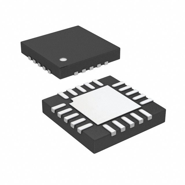
nn 20-Lead QFN 4mm × 4mm Package
The LTC®4318 enables the hardwired address of one or
more I2C or SMBus slave devices to be translated to a
different address. This allows slaves with the same hardwired address to coexist on the same bus. Only discrete
resistors are needed to select the new address and no
software programming is required. Up to 127 different
address translations are available.
nn
The LTC4318 incorporates a pass-through mode which
disables the address translations and allows general call
addressing by the master. The LTC4318 is designed to
automatically recover from abnormal bus conditions like
bus stuck low or premature STOP bits.
NUMBER OF INPUT
CHANNELS
NUMBER OF OUTPUT
CHANNELS
LTC4316
1
1
LTC4317
1
2
LTC4318
2
2
PART NUMBER
Applications
I2C, SMBus Address Expansion
nn Address Translation
nn Servers
nn Telecom
nn
L, LT, LTC, LTM, Linear Technology and the Linear logo are registered trademarks of Linear
Technology Corporation. All other trademarks are the property of their respective owners.
Protected by U.S. Patents, including 6356140, 6650174, 7032051, 7478286. Patent pending.
Typical Application
3.3V
5V
TRANSLATES
VCC
BY 0x02
SCLIN1 SCLOUT1
SCL
MASTER #1
SDA
SDAIN1
SENDS
ADDRESS 0x34
3.3V
SCL
SCL
SLAVE# 1
RECEIVES
ADDRESS 0X36
LTC4318
ENABLE1
READY1
ENABLE2
READY2
SCLIN2
SCLOUT2
SDAIN2
SDAOUT2
5V
TRANSLATES
BY 0x04
SCL
SLAVE# 2
MASTER #1
SDA
SENDS
ADDRESS 0x32
ADDRESS BITS
R/W
BIT
ACK
BIT
a6
a5
a4
a3
a2
a1
a0
SDAIN1
0
0
1
1
0
1
0
0
= 0x34
TRANSLATION
BYTE
0
0
0
0
0
0
1
0
= 0x02
SDAOUT1
0
0
1
1
0
1
1
0
SCLIN1
SDA
XORH2
= 0x36
4318 TA01b
RECEIVES
ADDRESS 0X36
XORH1
GND
START
SDA
SDAOUT1
XORL2 XORL1
3.3V
845k
61.9k
93.1k
4318 TA01a
4318fa
For more information www.linear.com/LTC4318
1
�LTC4318
Absolute Maximum Ratings
Pin Configuration
(Notes 1, 2)
SCLIN2
SCLOUT2
NC
GND
ENABLE2
TOP VIEW
20 19 18 17 16
15 SCLIN1
XORH2 1
XORL2 2
14 SCLOUT1
21
GND
XORH1 3
XORL1 4
13 SDAOUT1
12 SDAIN1
11 SDAIN2
8
READY1
9 10
SDAOUT2
7
NC
6
READY2
VCC 5
ENABLE1
Input Supply Voltage VCC.............................. –0.3V to 6V
Input Voltages
ENABLEn....................................................... –0.3V to 6V
XORLn, XORHn.................................–0.3V to VCC + 0.3V
Output Voltages
READYn........................................................ –0.3V to 6V
Output Currents
READYn, SDAOUTn.................................................50mA
Input/Output Voltages
SCLINn, SCLOUTn, SDAINn, SDAOUTn......... –0.3V to 6V
Operating Temperature Range
LTC4318C................................................. 0°C to 70°C
LTC4318I..............................................–40°C to 85°C
Storage Temperature Range................... –65°C to 150°C
UF PACKAGE
20-LEAD (4mm × 4mm) PLASTIC QFN
TJMAX = 150°C,θJA = 37°C/W
EXPOSED PAD (PIN 21) IS GND, PCB CONNECTION OPTIONAL
Order Information
LEAD FREE FINISH
TAPE AND REEL
PART MARKING*
PACKAGE DESCRIPTION
TEMPERATURE RANGE
LTC4318CUF#PBF
LTC4318CUF#TRPBF
4318
20-Lead (4mm × 4mm) Plastic QFN
0°C to 70°C
LTC4318IUF#PBF
LTC4318IUF#TRPBF
4318
20-Lead (4mm × 4mm) Plastic QFN
–40°C to 85°C
Consult LTC Marketing for parts specified with wider operating temperature ranges. *The temperature grade is identified by a label on the shipping container.
For more information on lead free part marking, go to: http://www.linear.com/leadfree/
For more information on tape and reel specifications, go to: http://www.linear.com/tapeandreel/. Some packages are available in 500 unit reels through
designated sales channels with #TRMPBF suffix.
2
4318fa
For more information www.linear.com/LTC4318
�LTC4318
Electrical Characteristics
The l denotes the specifications which apply over the full operating
temperature range, otherwise specifications are at TA = 25°C. VCC = 3.3V, unless otherwise specified.
SYMBOL
PARAMETER
CONDITIONS
MIN
TYP
MAX
UNITS
Supply
VCC
Input Supply Range
ICC
Input Supply Current
l
VCC(UVLO)
VCC Supply Undervoltage Lockout
VCC(HYST)
VCC Supply Undervoltage Lockout Hysteresis
2.25
5.5
V
ENABLE = 3.3V, SCLIN = SDAIN = 0V
l
0.8
2
mA
ENABLE = 0V, SCLIN = SDAIN = 0V
l
350
800
µA
VCC Rising
l
2.1
2.2
1.9
100
V
mV
ENABLE and READY
VENABLE(TH)
ENABLE Threshold Voltage
VENABLE(HYST)
ENABLE Hysteresis
Enable Rising
l
1
1.4
1.8
50
V
mV
IENABLE(LEAK)
ENABLE Input Current
l
±1
µA
VREADY(OL)
READY Output Low Voltage
I = 3mA
l
0.4
V
IREADY(OH)
READY Off Leakage Current
VCC = VREADY = 5.5V
l
±5
µA
SDA, SCL Pins Rising
l
2.0
V
SDA, SCL Pins = 5.5V, 0V, VCC = 5.5V,0V
l
±10
µA
SDAIN, SCLIN Pins = 5.5V, VCC = 5.5V,
SDAOUT, SCLOUT Pins = 4.5V
l
±10
µA
Note 3
l
10
pF
1.2
V
SCLIN, SDAIN, SCLOUT, SDAOUT
VSCL,SDA(TH)
Threshold Voltage
VSCL,SDA(HYST)
Hysteresis
ISCL,SDA(LEAK)
Leakage Current
ISCL,SDA(LEAK-INOUT) Input to Output Leakage Current
1.5
1.8
50
CSCL,SDA
Pin Capacitance
VSCL,SDA(PRE)
Precharge Voltage
VSDAOUT(OL)
SDAOUT Output Low Voltage
I = 4mA
l
RDS(ON)
Pass Switch On Resistance
VCC = 2.25V, SCLIN = SDAIN = 0.4V
VCC = 3.3V, SCLIN = SDAIN = 0.4V
VCC = 5V, SCLIN = SDAIN = 0.4V
l
l
l
l
0.8
1
3
2.2
1.8
mV
0.4
V
12
8
6
Ω
Ω
Ω
±100
nA
XORH, XORL
IXORH/XORL
XORH and XORL Input Current
l
I2C Interface Timing
fSCL(MAX)
Maximum SCLIN Clock Frequency
Note 3
l
tPDHL(SDAOUTn)
SDAOUT Fall Delay
C = 100pF, RPULLUP = 10k
l
400
kHz
170
300
ns
tf(SDAOUTn)
SDAOUT Fall Time
C = 100pF, RPULLUP = 10k
l
20
60
300
ns
tTIMEOUT
Stuck Bus Timeout
SCLIN Held Low or High
l
25
30
35
ms
tIDLE
Bus Idle Time
l
80
120
160
µs
tGLITCH
SCLIN and SDAIN Glitch Filter
l
50
100
Note 1: Stresses beyond those listed under Absolute Maximum Ratings
may cause permanent damage to the device. Exposure to any Absolute
Maximum Rating condition for extended periods may affect device
reliability and lifetime.
ns
Note 2: All currents into pins are positive and all voltages are referenced to
GND unless otherwise indicated.
Note 3: Guaranteed by design and not tested.
4318fa
For more information www.linear.com/LTC4318
3
�LTC4318
Timing Diagram
SDAIN
50%
SDAOUT
tPDHL(SDAOUT)
70%
50%
30%
tf(SDAOUT)
4318 EC
Typical Performance Characteristics
Standby Supply Current vs
Temperature
Supply Current vs Temperature
800
ENABLE = VCC
700
VCC = 5V
ICC (μA)
VCC = 2.25V
4
400
300
3
TA = 85°C
2
–25
0
25
50
TEMPERATURE (°C)
75
0
–50
100
–25
0
25
50
TEMPERATURE (°C)
75
Pass Switch-On Resistance vs
Temperature
READY Output Low
Voltage vs Current
100
SDAIN = SCLIN = 0.4V
5
VREADY(OL) (mV)
3
VCC = 3.3V
2
VCC = 5V
TA = 85°C
TA = 25°C
40
TA = –40°C
20
1
0
–50
240
220
60
–25
0
25
50
TEMPERATURE (°C)
75
100
4318 G04
0
3.0
3.5
VCC (V)
4.0
4.5
5.0
4318 G03
SDAOUT Fall Delay vs
Temperature
VCC = 3.3V
80
VCC = 2.25V
2.5
4318 G02
4318 G01
4
0
2.0
100
tPDHL(SDAOUT) (ns)
0.6
–50
TA = –40°C
1
100
RDS(ON) (Ω)
TA = 25°C
200
0.7
4
SDAIN = SCLIN = 0.4V
5
500
VCC = 3.3V
0.8
6
Pass Switch-On Resistance vs
VCC
600
0.9
ICC (mA)
6
ENABLE = 0V
RDS(ON) (Ω)
1.0
TA = 25°C, VCC = 3.3V unless otherwise noted.
VCC = 3.3V
C = 100pF
200
180
160
140
120
0
2
4
6
IREADY (mA)
10
8
4318 G05
100
–50
–25
0
25
50
TEMPERATURE (°C)
75
100
4318 G06
4318fa
For more information www.linear.com/LTC4318
�LTC4318
Typical Performance Characteristics
SDAOUT Fall Delay vs Bus
Capacitance
TA = 25°C, VCC = 3.3V unless otherwise noted.
SDAOUT Fall Time vs
Temperature
300
120
SDAOUT Fall Time vs Bus
Capacitance
120
C = 100pF
275
100
VCC = 2.25V
200
175
150
80
VCC = 3.3V
60
40
0
200
400
600
CBUS (pF)
800
1000
20
–50
–25
0
25
50
TEMPERATURE (°C)
4318 G07
VCC = 5V
80
VCC = 3.3V
60
VCC = 2.25V
40
VCC = 2.25V
125
100
tf(SDAOUT) (ns)
VCC = 3.3V
225
100
VCC = 5V
VCC = 5V
tf(SDAOUT) (ns)
tPDHL(SDAOUT) (ns)
250
75
100
4318 G08
20
0
200
400
600
CBUS (pF)
800
1000
4318 G09
Pin Functions
XORL1/XORL2: Translator XOR Lower Nibble Configuration Input. The DC voltage at this pin configures the lower
4-bit nibble of the address translation byte. Tie the pin to
an external resistive divider connected between VCC and
GND to set the desired DC voltage.
XORH1/XORH2: Translator XOR Upper Nibble Configuration Input. The DC voltage at this pin configures the upper
3-bit nibble of the address translation byte. Tie the pin to
an external resistive divider connected between VCC and
GND to set the desired DC voltage. Connect this pin to VCC
to activate pass-through mode. See Application Information section for more details.
ENABLE1/ENABLE2: Enable Input. If ENABLE pin is low,
the address translation is disabled, SDAIN is disconnected
from SDAOUT, and SCLIN is disconnected from SCLOUT.
A low to high transition on ENABLE restarts the configuration of the address translation byte and also enables the
address translation. Connect to VCC if unused.
Exposed Pad: Exposed pad may be left open or connected
to device GND.
GND: Device Ground.
READY1/READY2: Ready Status Output. This is an open
drain output to indicate that the device is ready for address
translation. The pin releases high when the LTC4318 has
completed configuration of the address translation byte,
SDAIN is connected to SDAOUT and SCLIN is connected
to SCLOUT. Connect a pull-up resistor, typically 10k, from
this pin to the bus pull-up supply. Leave open or tie to
GND if unused.
SCLIN1/SCLIN2: Input Bus Clock Input and Output. Connect this pin to the SCL line on the master side. An external
pull-up resistor or current source is required. Connect to
VCC through a pull-up resistor if unused.
SCLOUT1/SCLOUT2: Output Bus Clock Input and Output.
Connect this pin to the SCL line on the slave side. An external
pull-up resistor or current source is required. Connect to
VCC through a pull-up resistor if unused.
SDAIN1/SDAIN2: Input Bus Data Input and Output. Connect
this pin to the SDA line on the master side. An external
pull-up resistor or current source is required. Connect to
VCC through a pull-up resistor if unused.
SDAOUT1/SDAOUT2: Output Bus Data Input and Output.
Connect this pin to the SDA line on the slave side. An
external pull-up resistor or current source is required.
Connect to VCC through a pull-up resistor if unused.
VCC: Power Supply Input (2.25V to 5.5V). If the supply
voltages for the input and output buses are different, connect this pin to the lower supply. If the input and output
supplies have the same nominal value and with tolerance
less than or equal to ±10%, connect VCC to either supply.
Bypass with at least 0.1µF to GND.
For more information www.linear.com/LTC4318
4318fa
5
�LTC4318
Block Diagram
VCC
1V
1V
1V
PRECHARGE
PRECHARGE
200k
200k
SCLIN1
PRECHARGE
1V
PRECHARGE
200k
N1
200k
SCLOUT1
SCLOUT2
SCLIN2
SDAIN1
SDAOUT1
N2
SDAIN2
+
1.8V
SDAOUT2
CMP2
–
7-BIT
ADDRESS
TRANSLATION
BYTE
XOR
N3
CMP4
GLITCH
FILTER
+
1.8V
–
CMP1
CMP3
GLITCH
FILTER
–
+
I2C Hot
Swap
LOGIC
XORH1
CONTROL
LOGIC
+
–
I2C Hot
Swap
LOGIC
1.8V
1.8V
READY1
N4
READY2
XORH2
XORL1
XORL2
+
CMP6
CMP5
ENABLE1
+
ENABLE2
VCC/2
–
PRECHARGE
–
1.4V
GND
4318 BD
6
4318fa
For more information www.linear.com/LTC4318
�LTC4318
Operation
SCLIN to SCLOUT while N2 connects SDAIN to SDAOUT.
In most conditions, N1 and N2 stay on so that the input
and output buses are connected.
The LTC4318 is an I2C/SMBus address translator. It bridges
two segments of an I2C bus, reading incoming addresses
on the master side and retransmitting them to the slave
side with the 7-bit I2C addresses translated in real time.
This allows multiple I2C devices with the same address
to be connected to the same bus without interference.
The translated addresses are configured with external
resistors, and no extra software is required. An ENABLE
pin allows bus segments to be enabled and disabled, and
the LTC4318 allows hot swapping isolated bus segments
together.
Translation starts when the master issues a START bit
(SDAIN goes low while SCLIN is high). The LTC4318
turns off N2 to disconnect SDAIN from SDAOUT. As the
master sends the address byte, the LTC4318 translates
the incoming address at the SDAIN pin to a new address
at the SDAOUT pin by XORing each incoming bit with
a user-configurable translation byte, one bit at a time.
N3 turns on and off to send out the new address to the
SDAOUT pin. Once all 7 bits of the address are processed,
the LTC4318 turns on N2 again to reconnect SDAIN to
SDAOUT. The master then transmits the R/W bit directly
to the slave. If the new, translated address on SDAOUT
matches the slave’s address, the slave pulls SDAOUT low
to acknowledge (ACK bit). N2 remains on and the rest of
the data bytes are transmitted unmodified between the
master and slave. The address translation process restarts
when the master issues a new START bit.
Figure 1 shows an I2C master connected to the input bus
of the LTC4318 (SCLIN and SDAIN). The slave devices
requiring address translation are connected to the output
bus of the LTC4318 (SCLOUT and SDAOUT). Any other
slave devices that do not require address translation are
placed together with the master on the input bus of the
LTC4318. Two switches (N1 and N2) inside the LTC4318
connect the input bus to the output bus. N1 connects
VCC1
VCC2
LTC4318
N1
SCLIN
SCLOUT
MASTER
N2
SDAIN
+
SLAVE
#2
1.8V
–
SDAOUT
SLAVE
#1
CMP2
N3
XOR
0 0 0 0 0 1 0
ENABLE
7-BIT ADDRESS
ADDRESS
TRANSLATION
TRANSLATION
BYTE SHIFT REGISTER
4318 F01
Figure 1. Basic Functions of the LTC4318
4318fa
For more information www.linear.com/LTC4318
7
�LTC4318
Operation
Figure 2 shows typical waveforms for the circuit on the
front page. In this example, the master transmits address
0x34 while the slave is configured to respond to address
0x36. The resistive dividers at the XORL and XORH pins are
configured to generate an address translation byte of 0x02.
START
Note that in this example, the 8-bit hexadecimal address
format (with R/W = 0) is used. 7-bit addresses are also
commonly found in I2C device documentation. Make sure
to use the correct format when calculating the address
translation byte. Table 1 shows examples of both formats.
ADDRESS BITS
R/W
BIT
ACK
BIT
a6
a5
a4
a3
a2
a1
a0
SDAIN
0
0
1
1
0
1
0
0
= 0x34
TRANSLATION
BYTE
0
0
0
0
0
0
1
0
= 0x02
SDAOUT
0
0
1
1
0
1
1
0
= 0x36
SCLIN
N2 GATE N2 ON
N2 OFF
N2 ON
4318 F02
Figure 2. Basic Address Translation Waveforms
Table 1.
DESCRIPTION
Input Address from SDAIN
Translation Byte
Output Address to SDAOUT
8
a6
0
0
0
a5
0
0
0
a4
1
0
1
BINARY ADDRESS
a3
a2
1
0
0
0
1
0
a1
1
0
1
a0
0
1
1
R/W
0
0
0
7-BIT HEX ADDRESS
WITHOUT R/W
8-BIT HEX ADDRESS
WITH R/W = 0
0x1A
0x01
0x1B
0x34
0x02
0x36
4318fa
For more information www.linear.com/LTC4318
�LTC4318
Operation
System Configurations
There are several ways that individual slaves or banks of
slaves can be connected to an LTC4318. In Figure 3, each
slave is paired with one channel of the LTC4318. This
configuration allows for maximum flexibility in allocating
the bus addresses. Both read and write operations and all
protocols supported by the LTC4318 are allowed. Figure 4
shows two slaves with different hardwired addresses
translated to two different addresses using one channel of
the LTC4318 and a common translation byte. A program
is available to help the user visualize an I2C bus with the
LTC4318; this program can be found in the following link:
www.linear.com/TranslatorTool
7-bit translation byte. These voltages are referenced to
VCC so a resistive divider at each of these pins is the most
convenient way to set the voltages. The required translation byte can be determined by taking the bitwise XOR of
the slave’s original address and the desired input address.
The voltages at the XORH and XORL pins configure the
translation byte. The XORL voltage configures the lower 4
translation bits (excluding the R/W bit), while the XORH
voltage configures the upper 3 translation bits. Tables 2
and 3 show the recommended resistive divider values. RLT
and RLB are the top and bottom resistors connected to
XORL, while RHT and RHB are the top and bottom resistors
connected to XORH (Figure 5). Use 1% tolerance resistors
for RLT, RLB, RHT and RHB.
Setting the Translation Byte
When the LTC4318 is first powered up or any time a rising
edge is detected on the ENABLE pin, the LTC4318 reads
the voltages at the XORH and XORL pins to determine the
SCL
SLAVE
#2
SDA
SLAVE #1
INPUT ADDRESS
0x32
TRANSLATION BYTE
0x06
SCLIN1
SCLOUT1
LTC4318
SDAIN1
SDAOUT1
HARDWIRED ADDRESS
0x34
SCL
SCLIN
MASTER
SCL
SDAIN
SLAVE
#1
SDA
SCLOUT2
00110010
00000110
00110100
SDAIN2
SCL
MASTER
SDA
SDAOUT2
SLAVE #3
INPUT ADDRESS
0x36
TRANSLATION BYTE
0x02
SDA
00110110
00000010
00110100
SDA
HARDWIRED ADDRESS
0x34
SCL
SLAVE
#3
SLAVE #3
INPUT ADDRESS
0x32
00110010
00000010
00110000
SDA
HARDWIRED ADDRESS
0x30
4318 F04
Figure 4. Two Slaves Sharing One Channel of LTC4318
VCC
SCL
RHT
SLAVE
#2
VCC
RHB
4318 F03
Figure 3. Two Independent Address Translation
RLT
LTC4318
XORH
SDA
HARDWIRED ADDRESS
0x34
SDAOUT
SLAVE #1
INPUT ADDRESS
0x36
00110110
00000010
00110100
HARDWIRED ADDRESS
0x34
SLAVE
#1
TRANSLATION BYTE
0x02
SCL
SLAVE
#3
SCL
LTC4318
SDA
HARDWIRED ADDRESS
0x34
SCLIN2
SCLOUT
XORL
RLB
4318 F05
Figure 5. Address Translation Byte Configuration Resistors
4318fa
For more information www.linear.com/LTC4318
9
�LTC4318
Operation
Table 2. Setting the Resistive Divider at XORL
LOWER
4-BIT OF
TRANSLATION
BYTE
RECOMMENDED RECOMMENDED
RLT [kΩ]
RLB [kΩ]
a3 a2 a1 a0
VXORL/VCC
0 0 0
0
≤ 0.03125
Open
Short
0 0 0
1
0.09375 ±0.015
976
102
0 0 1
0
0.15625 ±0.015
976
182
0 0 1
1
0.21875 ±0.015
1000
280
0 1 0
0
0.28125 ±0.015
1000
392
0 1 0
1
0.34375 ±0.015
1000
523
0 1 1
0
0.40625 ±0.015
1000
681
0 1 1
1
0.46875 ±0.015
1000
887
1 0 0
0
0.53125 ±0.015
887
1000
1 0 0
1
0.59375 ±0.015
681
1000
1 0 1
0
0.65625 ±0.015
523
1000
1 0 1
1
0.71875 ±0.015
392
1000
1 1 0
0
0.78125 ±0.015
280
1000
1 1 0
1
0.84375 ±0.015
182
976
1 1 1
0
0.90625 ±0.015
102
976
1 1 1
1
≥ 0.96875
Short
Open
which gives 0110 0010b or 0x62. If the configuration
voltages at XORL and XORH pins are the same, they can
be tied together and connected to a single resistive divider.
Alternatively, three resistors can be used to configure
the XORL and XORH pins (Figure 6). Use the following
procedure to calculate the value of the three resistors:
VCC
RA1
VCC
XORL
LTC4318
RA2
XORH
RA3
4318 F06
Figure 6. Address Translation Byte
Configuration Using Three Resistors
First choose a total resistance value RTOTAL
RA3 = RTOTAL • (VXORH/VCC)
RA2 = (RTOTAL • VXORL/VCC) – RA3
Table 3. Setting the Resistive Divider at XORH
UPPER
3-BIT OF
TRANSLATION
BYTE
a6
a5
a4
RA1 = RTOTAL – RA3 – RA2
Use 1% tolerance resistors for RA1, RA2 and RA3.
VXORH/VCC
RECOMMENDED RECOMMENDED
RHT {kΩ]
RHB [kΩ}
0
0
0
≤ 0.03125
Open
Short
0
0
1
0.09375 ±0.015
976
102
0
1
0
0.15625 ±0.015
976
182
0
1
1
0.21875 ±0.015
1000
280
1
0
0
0.28125 ±0.015
1000
392
1
0
1
0.34375 ±0.015
1000
523
1
1
0
0.40625 ±0.015
1000
681
1
1
1
0.46875 ±0.015
1000
887
For example, if RLT = 976k, RLB = 102k, RHT = 1000k, and
RHB = 280k, the lower 4 translation bits are 0001b and
the upper 3 bits are 011b. The 8-bit hexadecimal address
translation byte is obtained by adding a 0 as the LSB,
10
Once the XORL and XORH pins are read, the LTC4318
turns on switches N1 and N2, connecting the input and
output, and the READY pin goes high to indicate that the
LTC4318 is ready to start address translation.
The address translation byte can be changed during
operation by changing the XORH and XORL voltages and
toggling the ENABLE pin (high-low-high). This triggers
the LTC4318 to re-read the XORL and XORH voltages.
Enable/UVLO
If the ENABLE pin is driven below 1.4V or if VCC is below the UVLO threshold, the LTC4318 shuts down. The
internal shift register storing the address translation byte
is cleared, address translation is disabled, switches N1,
N2 and N3 are off, the READY pin is pulled low and the
quiescent current drops to 350µA.
4318fa
For more information www.linear.com/LTC4318
�LTC4318
Operation
Precharge and Hot Swap
ADDRESS BITS
When the LTC4318 is first powered on, switches N1 and
N2 are initially off. This allows a LTC4318 and its connected slaves to be hot swapped onto an active I2C bus.
Internal precharge circuitry initially sets the bus lines to
1V through a 200k resistor, minimizing disturbance to an
active bus when the LTC4318 is connected. The LTC4318
keeps N1 and N2 off until ENABLE goes high, the XORL/
XORH pins are read, and both sides of the I2C bus are
idle (indicated either by a STOP bit or all bus pins high
for longer than 120µs). Once these conditions are met, N1
and N2 turn on, and the READY pin goes high to indicate
that the LTC4318 is ready to start address translation.
Pass-Through Mode
If the master wants to communicate with the slave using the general call address, it can temporarily disable
address translation by pulling XORH high. This disables
address translation and keeps N1 and N2 on regardless
of the activity on the buses. Any translation that may be in
progress is stopped immediately when XORH goes high.
Extra Transitions on SDAOUT
SCLIN
SDAIN
0
1
0
1
TRANSLATION
BYTE
0
1
1
0
SDAOUT
0
0
1
1
N2 GATE
Level Translation and Supply Voltage Matching
The LTC4318 can operate with different supply voltages
on the input and output bus, and it will level shift the
voltages on the SCLIN, SDAIN, SCLOUT, and SDAOUT
pins to match the supply voltage at each side. VCC must
be powered from the lower of the two supply voltages
N2 OFF
GLITCH
4318 F07
Figure 7. Extra Transitions on SDAOUT While SCL Is Low
for level shifting to operate correctly. For example, if the
input bus is powered by a 5V supply and the output bus
is powered by a 3.3V supply, the LTC4318 VCC pin must
be connected to the 3.3V supply as shown in Figure 8.
If the LTC4318 supply pin is connected to the higher bus
supply, current may flow through the switches N1 and
5V
3.3V
VCC
SCLIN
SCLOUT
SLAVE
#1
LTC4318
MASTER
In an I2C/SMBus system, the master changes the state of
the SDA line when SCL is low. The LTC4318 also advances
the address translation byte shift register when the SCLIN
is low. The translation byte transitions occur approximately
100ns after the falling edge of SCLIN. If the SDAIN transitions sent by the master do not coincide exactly with
the LTC4318 address translation bit transitions, an extra
transition on SDAOUT may appear (Figure 7). These extra
SDA transitions are like glitches similar to those occurring
during normal Acknowledge bit transitions and do not pose
problems in the system because devices on the bus latch
SDA data only when SCL is high.
GLITCH
SDAIN
SDAOUT
4318 F08
Figure 8. A 5V to 3.3V Level Translation Application
N2 to the bus with lower supply. If the voltage difference
is less than 1V, this current is limited to less than 10µA.
This allows the input and output buses to be connected
to nominally identical supplies that may have up ±10%
tolerance, and the LTC4318 VCC pin can be connected to
either supply.
Extra START and STOP Bits
During normal operation, an I2C master should not issue
a START or STOP bit within a data byte. I2C slave behavior
when such a command is received can be unpredictable.
The LTC4318 will recover automatically when an unexpected START or STOP is received during the address byte;
however, depending on the state of the translating bits,
it may convert START bits to STOP bits and vice versa,
causing unexpected slave behavior.
4318fa
For more information www.linear.com/LTC4318
11
�LTC4318
Operation
If a START bit is received during the address byte when
the active translating bit is a "1", the slave device will see
a STOP bit. This will typically reset the slave and cause it
to miss the remainder of the transmission. If the START
bit is received while the active translating bit is a "0", the
START passes through the LTC4318 unchanged. The slave
will react in the same way it would if the LTC4318 was
not present, and will typically reset when the master next
issues a STOP bit. In both cases, the LTC4318 automatically resets at the next STOP bit and the next message
will be transmitted normally.
If a STOP bit is received during the address byte, the
LTC4318 will abort the address translation and ensure that
a STOP bit is issued at SDAOUT to reset the slave. If the
active translating bit is a "0" when the STOP arrives, it is
not modified, and the slave will see the STOP and typically
reset. If the active translating bit is a "1" when the STOP
arrives, the slave device will see a START bit. This might
leave the slave in an indeterminate state, so the LTC4318
briefly disconnects the slave from the master, adds a short
delay, and then generates a STOP bit at the SDAOUT pin
(Figure 9). It then reconnects the busses and waits for a
START bit to begin the next transmission. Again, in both
cases, the LTC4318 automatically resets and the next
message will be transmitted normally.
TRANSLATION
BIT
N2 GATE
Write Byte/Word
Read Byte/Word
Process Call
Block Write/Read
Block Write-Block Read Process Call
Extended Read and Write Commands
General Call (I2C Only)
START
BIT
Ultra Fast-Mode I2C Bus Protocol
START
BIT
N2 OFF
Unsupported SMBus Protocols:
SMBus Host Notify
N2 OFF
N1
OFF
Address Resolution Protocol (ARP)
N1 ON
4318 F09
Figure 9. Stop Bit within Address Byte when
Address Translation Byte Is 1
12
Send/Receive Byte
Device ID
N2 ON
N1 GATE
Supported I2C and SMBus Protocols:
10-Bit Addressing
1
N1 ON
The LTC4318 is designed to support most I2C and SMBus
message protocols. The only exceptions are protocols that
use pre-assigned addresses on the slave side of the bus.
Unsupported I2C Protocols:
START
BIT
STOP
BIT
SDAOUT
Supported Protocols
PMBus (without PEC)
SCLIN
SDAIN
During the address translation, if SCLIN stays low or high
for more than 30ms without any transitions, the LTC4318
will abort the address translation and reconnect SDAIN
to SDAOUT. It will then wait for a START bit to start a new
address translation. This prevents any bus stuck low/
high conditions from permanently disconnecting SDAIN
from SDAOUT.
Start Byte (I2C Only)
ADDRESS BIT
BECOMES
STOP BIT
STOP
BIT
Stuck Bus Timeout
Parity Error Code (PEC)
Alert Response Address (ARA)
PMBus (with PEC)
4318fa
For more information www.linear.com/LTC4318
�LTC4318
Typical Applications
INPUT ADDRESS
0x32
MOTHERBOARD
CONNECTOR 1
VCC
10k
10k
TO MASTER1 SCL
SCLIN1
TO MASTER1 SDA
SDAIN1
VCC
ENABLE1
10k
PLUG-IN
CARD 1
VCC
TO SLAVE #1
HARDWIRED
ADDRESS
SCL1 0x30
VCC
10k
10k
SCLOUT1
VCC
10k
SDAOUT1
10k
TO MASTER2 SCL
SCLIN2
TO MASTER2 SDA
SDAIN2
SDA1
GND
LTC4318
ENABLE2
10k
VCC
10k
VCC
10k
READY1
SCLOUT2
READY2
SDAOUT2
TO SLAVE #2
HARDWIRED
ADDRESS
SCL2 0x30
VCC
10k
10k
SDA2
GND
XORL2 XORL1 XORH2 XORH1
VCC
845k
61.90k
93.1k
MOTHERBOARD
CONNECTOR 2
PLUG-IN
CARD 2
INPUT ADDRESS
0x34
4318 F10
Figure 10. LTC4318 with Address Translation Byte of 0x02 and 0x04
4318fa
For more information www.linear.com/LTC4318
13
�LTC4318
Package Description
Please refer to http://www.linear.com/product/LTC4318#packaging for the most recent package drawings.
UF Package
20-Lead Plastic QFN (4mm × 4mm)
(Reference LTC DWG # 05-08-1710 Rev A)
0.70 ±0.05
4.50 ±0.05
3.10 ±0.05
2.00 REF
2.45 ±0.05
2.45 ±0.05
PACKAGE OUTLINE
0.25 ±0.05
0.50 BSC
RECOMMENDED SOLDER PAD PITCH AND DIMENSIONS
APPLY SOLDER MASK TO AREAS THAT ARE NOT SOLDERED
4.00 ±0.10
0.75 ±0.05
BOTTOM VIEW—EXPOSED PAD
R = 0.05
TYP
R = 0.115
TYP
19 20
0.40 ±0.10
PIN 1
TOP MARK
(NOTE 6)
4.00 ±0.10
PIN 1 NOTCH
R = 0.20 TYP
OR 0.35 × 45°
CHAMFER
1
2.00 REF
2.45 ±0.10
2
2.45 ±0.10
(UF20) QFN 01-07 REV A
0.200 REF
0.00 – 0.05
0.25 ±0.05
0.50 BSC
NOTE:
1. DRAWING IS PROPOSED TO BE MADE A JEDEC PACKAGE OUTLINE MO-220
VARIATION (WGGD-1)—TO BE APPROVED
2. DRAWING NOT TO SCALE
3. ALL DIMENSIONS ARE IN MILLIMETERS
4. DIMENSIONS OF EXPOSED PAD ON BOTTOM OF PACKAGE DO NOT INCLUDE
MOLD FLASH. MOLD FLASH, IF PRESENT, SHALL NOT EXCEED 0.15mm ON ANY SIDE
5. EXPOSED PAD SHALL BE SOLDER PLATED
6. SHADED AREA IS ONLY A REFERENCE FOR PIN 1 LOCATION
ON THE TOP AND BOTTOM OF PACKAGE
14
4318fa
For more information www.linear.com/LTC4318
�LTC4318
Revision History
REV
DATE
DESCRIPTION
A
10/15
Minor edits
PAGE NUMBER
4, 5
4318fa
Information furnished by Linear Technology Corporation is believed to be accurate and reliable.
However, no responsibility is assumed for its use. Linear Technology Corporation makes no representation that the interconnection
of its circuits
as described
herein will not infringe on existing patent rights.
For more
information
www.linear.com/LTC4318
15
�LTC4318
Typical Application
SINGLE
LTC4316
“Y” CONNECTED DUAL
LTC4317
VCC
DUAL
LTC4318
VCC
VCC
SCLIN
SCLIN
SCLOUT
SCLOUT
SCLIN
SCLIN
SCLOUT
SCLOUT1
SCLIN1
SCLIN
SCLOUT
SCLOUT1
SDAIN
SDAIN SDAOUT
SDAOUT
SDAIN
SDAIN SDAOUT
SDAOUT1
SDAIN1
SDAIN SDAOUT
SDAOUT1
XORH
XORH
READY
XORH1
XORH
READY1
XORH1
XORH
READY1
XORL
XORL
XORL1
XORL
XORL1
XORL
ENABLE
READY
ENABLE
ENABLE1
READY
ENABLE1
ENABLE
CHANNEL1
GND
SCLOUT2
SCLIN2
SCLIN
SCLOUT
SCLOUT2
SDAIN SDAOUT
SDAOUT2
SDAIN2
SDAIN SDAOUT
SDAOUT2
READY2
XORH2
XORH
READY2
XORL2
XORL
XORH2
XORH
XORL2
XORL
READY
ENABLE
CHANNEL2
GND
ENABLE
CHANNEL1
SCLOUT
SCLIN
ENABLE2
READY
READY
ENABLE
CHANNEL2
ENABLE2
GND
4318 F11
Figure 11. Comparison Between LTC4316/LTC4317/LTC4318
Related Parts
PART NUMBER DESCRIPTION
COMMENTS
LTC4300A-1/
LTC4300A-2/
LTC4300A-3
Hot Swappable 2-Wire Bus Buffers
LTC4300A-1: Bus Buffer with READY and ENABLE
LTC4300A-2: Dual Supply Buffer with ACC
LTC4300A-3: Dual Supply Buffer and ENABLE
LTC4302-1/
LTC4302-2
Addressable 2-Wire Bus Buffer
Address Expansion, GPIO, Software Controlled
LTC4303/
LTC4304
Hot Swappable 2-Wire Bus Buffer with Stuck Provides Automatic Clocking to Free Stuck I2C Busses
Bus Recovery
LTC4305/
LTC4306
2- or 4-Channel, 2-Wire Bus Multiplexers
with Capacitance Buffering
Two or Four Software Selectable Downstream Busses, Stuck Bus Disconnect, Rise Time
Accelerators, Fault Reporting, ±10kV HBM ESD
LTC4307
Low Offset, Hot Swappable 2-Wire Bus
Buffer with Stuck Bus Recovery
60mV Buffer Offset, 30ms Stuck Bus Disconnect and Recovery, Rise Time Accelerators,
±5kV HBM ESD
LTC4307-1
High Definition Multimedia Interface (HDMI) 60mV Buffer Offset, 3.3V to 5V Level Shifting, ±5kV HBM ESD
Level Shifting 2-Wire Bus Buffer
LTC4308
Low Voltage, Level Shifting Hot Swappable
2-Wire Bus Buffer with Stuck Bus Recovery
Bus Buffer with 1V Precharge, ENABLE and READY, 0.9V to 5.5V Level Translation, 30ms
Stuck Bus Disconnect and Recovery, Output Side Rise Time Accelerators, ±6kV HBM ESD
LTC4309
Low Offset Hot Swappable 2-Wire Bus
Buffer with Stuck Bus Recovery
60mV Buffer Offset, 30ms Stuck Bus Disconnect and Recovery, Rise Time Accelerators,
±5kV HBM ESD, 1.8V to 5.5V Level Translation
LTC4310-1/
LTC4310-2
Hot Swappable I2C Isolators
Bidirectional I2C Communication Between Two Isolated Busses, LTC4310-1: 100kHz Bus,
LTC4310-2: 400kHz Bus
LTC4311
Hot Swappable I2C/SMBus Accelerator
Rise Time Acceleration with ENABLE, ±8kV HBM ESD
LTC4312/
LTC4314
2- or 4-Channel, Hardware Selectable 2-Wire Two or Four Pin Selectable Downstream Busses, VIL Up to 0.3V • VCC, Rise Time
Bus Multiplexers with Capacitance Buffering Accelerators, 45ms Stuck Bus Disconnect and Recovery, ±4kV HBM ESD
LTC4313-1/
LTC4313-2/
LTC4313-3
High Noise Margin 2-Wire Bus Buffers
VIL = 0.3V • VCC, Rise Time Accelerators, Stuck Bus Disconnect and Recovery, 1V
Precharge, ±4kV HBM ESD
16 Linear Technology Corporation
1630 McCarthy Blvd., Milpitas, CA 95035-7417
For more information www.linear.com/LTC4318
(408) 432-1900 ● FAX: (408) 434-0507
●
www.linear.com/LTC4318
4318fa
LT 1015 REV A • PRINTED IN USA
© LINEAR TECHNOLOGY CORPORATION 2015
�


 工商网监
湘ICP备2023018690号
工商网监
湘ICP备2023018690号
