LTC5532
Precision 300MHz to 7GHz
RF Detector with Gain
and Offset Adjustment
U
FEATURES
■
■
■
■
■
■
■
■
■
DESCRIPTIO
Temperature Compensated Internal Schottky
Diode RF Detector
Wide Input Frequency Range: 300MHz to 7GHz*
Wide Input Power Range: –32dBm to 10dBm
Buffered Detector Output with External Gain Control
Precision VOUT Offset Control
Low Starting Voltage: 120mV ±35mV for Gain = 2x
Wide VCC Range of 2.7V to 6V
Low Operating Current: 500µA
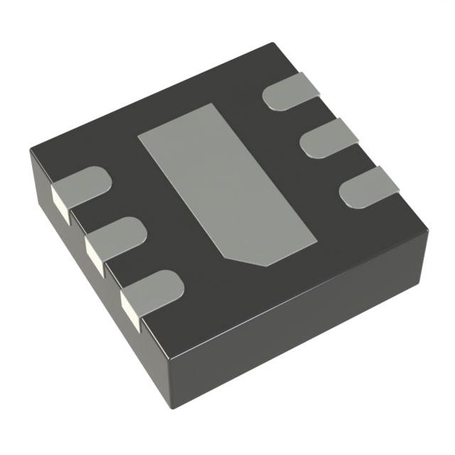
Available in a Low Profile (1mm) SOT-23 Package
and Tiny 6-Lead (2mm × 2mm) DFN Package
U
APPLICATIO S
■
■
■
■
■
■
802.11a, 802.11b, 802.11g, 802.15
Multimode Mobile Phone Products
Optical Data Links
Wireless Data Modems
Wireless and Cable Infrastructure
RF Power Alarm
Envelope Detector
The RF input voltage is peak detected using an on-chip
Schottky diode. The detected voltage is buffered and
supplied to the VOUT pin.
The LTC5532 output buffer gain is set via external resistors. The initial starting voltage of 120mV ±35mV can be
precisely adjusted using the VOS pin.
The LTC5532 operates with RF input power levels from
–32dBm to 10dBm.
, LTC and LT are registered trademarks of Linear Technology Corporation.
ThinSOT is a trademark of Linear Technology Corporation.
*Higher frequency operation is achievable with reduced performance. Consult factory for more
information.
U
■
The LTC®5532 is an RF power detector for RF applications
operating in the 300MHz to 7GHz range. A temperature
compensated Schottky diode peak detector and buffer
amplifier are combined in a small ThinSOTTM or (2mm ×
2mm) DFN package. The supply voltage range is optimized for operation from a single lithium-ion cell or 3×
NiMH.
TYPICAL APPLICATIO
Output Voltage vs RF Input Power
(SOT-23 Package)
3600
33pF
RF
INPUT
1
RFIN
VCC 6
VCC
100pF
LTC5532ES6
2
VOS
REFERENCE
3
GND
VOUT
5
RA
VOS
VM
4
RB
5532 TA01
0.1µF
VOUT OUTPUT VOLTAGE (mV)
300MHz to 7GHz RF Power Detector
(SOT-23 Package)
VCC = 3.6V
3200 TA = 25°C
GAIN = 2
2800 VOS = 0V
1000MHz
300MHz
2400
4000MHz
2000
1600
1200
800
400
2000MHz
3000MHz
5000MHz
6000MHz
7000MHz
0
–32 –27 –22 –17 –12 –7
–2
RF INPUT POWER (dBm)
3
8
5532 TA02
5532f
1
�LTC5532
W W
U
W
ABSOLUTE
AXI U RATI GS (Note 1)
VCC, VOUT, VM, VOS .................................. –0.3V to 6.5V
RFIN Voltage ......................................(VCC ± 1.5V) to 7V
RFIN Power (RMS) ............................................. 12dBm
IVOUT ...................................................................... 5mA
Operating Temperature Range (Note 2) .. – 40°C to 85°C
Maximum Junction Temperature ......................... 125°C
Storage Temperature Range ................ – 65°C to 125°C
Lead Temperature (Soldering, 10 sec)
SOT-23 Only ......................................................... 300°C
U
W
U
PACKAGE/ORDER I FOR ATIO
TOP VIEW
6 RFIN
VCC 1
VOUT 2
ORDER PART
NUMBER
7
VM 3
LTC5532EDC
5 GND
4 VOS
DC6 PACKAGE
6-LEAD (2mm × 2mm) PLASTIC DFN
TJMAX = 125°C, θJA = 85°C/W
EXPOSED PAD (PIN 7) IS GND,
MUST BE SOLDERED TO PCB
DC6 PART MARKING
LAFR
ORDER PART
NUMBER
TOP VIEW
RFIN 1
6 VCC
GND 2
5 VOUT
VOS 3
4 VM
LTC5532ES6
S6 PART MARKING
S6 PACKAGE
6-LEAD PLASTIC TSOT-23
LTAFS
TJMAX = 125°C, θJA = 250°C/W
Consult LTC Marketing for parts specified with wider operating temperature ranges.
ELECTRICAL CHARACTERISTICS
The ● denotes the specifications which apply over the full operating
temperature range, otherwise specifications are at TA = 25°C. VCC = 3.6V, RF Input Signal is Off, RA = RB = 1k, VOS = 0V unless
otherwise noted (Note 2).
PARAMETER
VCC Operating Voltage
IVCC Operating Current
VOUT VOL (No RF Input)
VOUT Output Current
VOUT Bandwidth
VOUT Load Capacitance
VOUT Slew Rate
VOUT Noise
VOS Voltage Range
VOS Input Current
VM Voltage Range
VM Input Current
RFIN Input Frequency Range
RFIN Input Power Range
RFIN AC Input Resistance
RFIN Input Shunt Capacitance
CONDITIONS
●
IVOUT = 0mA
RLOAD = 2k, VOS = 0V
VOUT = 1.75V, VCC = 2.7V, ∆VOUT < 10mV
CLOAD = 33pF, RLOAD = 2k (Note 4)
(Note 6)
VRFIN = 1V Step, CLOAD = 33pF, Total RLOAD = 2k (Note 3)
VCC = 3V, Noise BW = 1.5MHz, 50Ω RF Input Termination,
50Ω AC Output Termination
●
●
●
0.5
100 to 140
4
2
MAX
6
0.7
155
33
3
1
●
●
VM = 3.6V
●
(Note 7)
RF Frequency = 300MHz to 7GHz (Note 5, 6) VCC = 2.7V to 6V
F = 1000MHz, Pin = –25dBm
F = 1000MHz, Pin = –25dBm
Note 1: Absolute Maximum Ratings are those values beyond which the life
of a device may be impaired.
Note 2: Specifications over the –40°C to 85°C operating temperature
range are assured by design, characterization and correlation with
statistical process controls.
Note 3: The rise time at VOUT is measured between 1.3V and 2.3V.
85
2
TYP
●
●
VOS = 1V
MIN
2.7
0
–0.5
0
–0.5
1
0.5
VCC -1. 8
0.5
300 to 7000
–32 to 10
220
0.65
UNITS
V
mA
mV
mA
MHz
pF
V/µs
mVP-P
V
µA
V
µA
MHz
dBm
Ω
pF
Note 4: Bandwidth is calculated based on the 10% to 90% rise time
equation: BW = 0.35/rise time.
Note 5: RF performance is tested at 1800MHz
Note 6: Guaranteed by design.
Note 7: Higher frequency operation is achievable with reduced
performance. Consult factory for more information.
5532f
2
�LTC5532
U W
TYPICAL PERFOR A CE CHARACTERISTICS
unless otherwise indicated.
Output Voltage vs Supply Voltage
(RF Input Signal Off)
(RLOAD = 20k) Characteristics are for both packages
Supply Current vs Supply Voltage
(RF Input Signal Off)
130
Output Delay vs RF Input Power
500
1000
VCC = 3.6V
TA = 25°C
VOS = 0V
GAIN = 2
TA = 25°C
120
TA = –40°C
115
800
480
TA = –40°C
460
OUTPUT DELAY (ns)
TA = 85°C
125
SUPPLY CURRENT (µA)
TA = 25°C
TA = 85°C
440
110
2.5
3.0
3.5
4.0
4.5
5.0
SUPPLY VOLTAGE (V)
5.5
420
2.5
6.0
3.0
3.5
4.0
4.5
5.0
SUPPLY VOLTAGE (V)
5532 G01
50% SWITCHING
3600
VCC = 3.6V
VOUT OUTPUT VOLTAGE (mV)
TA = –40°C
2400
2000
TA = 25°C
1600
1200
800
TA = 85°C
400
0
–32 –28 –24 –20 –16 –12 –8 –4 0
RF INPUT POWER (dBm)
3600
2800
TA = –40°C
2400
2000
TA = 25°C
1600
1200
800
TA = 85°C
5532 G04
3600
VCC = 3.6V
VOUT OUTPUT VOLTAGE (mV)
2000
TA = 25°C
1200
800
400
TA = 85°C
0
–32 –28 –24 –20 –16 –12 –8 –4 0
RF INPUT POWER (dBm)
4
4
2000
5532 G07
TA = 25°C
1600
1200
800
TA = 85°C
0
–32 –28 –24 –20 –16 –12 –8 –4 0
RF INPUT POWER (dBm)
8
3600
TA = –40°C
TA = 25°C
1200
800
VCC = 3.6V
3200
2000
1600
8
5532 G06
VCC = 3.6V
2800
2400
4
Typical Detector Characteristics,
5000MHz, Gain = 2, VOS = 0V
(SOT-23 Package)
TA = 85°C
400
8
TA = –40°C
2400
400
3200
3200
1600
2800
Typical Detector Characteristics,
4000MHz, Gain = 2, VOS = 0V
TA = –40°C
VCC = 3.6V
5532 G05
Typical Detector Characteristics,
3000MHz, Gain = 2, VOS = 0V
10
3200
0
–32 –28 –24 –20 –16 –12 –8 –4 0
RF INPUT POWER (dBm)
8
2800
0
–5
5
RF INPUT POWER (dBm)
Typical Detector Characteristics,
2000MHz, Gain = 2, VOS = 0V
VCC = 3.6V
400
4
–10
5532 G03
3200
2800
2400
0
6.0
Typical Detector Characteristics,
1000MHz, Gain = 2, VOS = 0V
3200
3600
5.5
VOUT OUTPUT VOLTAGE (mV)
3600
VOUT OUTPUT VOLTAGE (mV)
90% SWITCHING
400
5532 G02
Typical Detector Characteristics,
300MHz, Gain = 2, VOS = 0V
VOUT OUTPUT VOLTAGE (mV)
600
200
VOUT OUTPUT VOLTAGE (mV)
VOUT OUTPUT VOLTAGE (mV)
VOS = 0V
GAIN = 2
0
–32 –28 –24 –20 –16 –12 –8 –4 0
RF INPUT POWER (dBm)
2800
2400
2000
1600
8
5532 G08
TA = 25°C
1200
800
400
4
TA = –40°C
TA = 85°C
0
–32 –28 –24 –20 –16 –12 –8 –4 0
RF INPUT POWER (dBm)
4
8
5532 G09
5532f
3
�LTC5532
U W
TYPICAL PERFOR A CE CHARACTERISTICS
unless otherwise indicated.
Typical Detector Characteristics,
6000MHz, Gain = 2, VOS = 0V
(SOT-23 Package)
Typical Detector Characteristics,
7000MHz, Gain = 2, VOS = 0V
(SOT-23 Package)
3600
VCC = 3.6V
3600
VCC = 3.6V
3200
VOUT OUTPUT VOLTAGE (mV)
3200
VOUT OUTPUT VOLTAGE (mV)
Typical Detector Characteristics,
300MHz, Gain = 4, VOS = 0V
2800
TA = –40°C
2400
2000
TA = 25°C
1600
1200
800
TA = 85°C
400
0
–32 –28 –24 –20 –16 –12 –8 –4 0
RF INPUT POWER (dBm)
4
2800
2400
TA = –40°C
2000
1600
TA = 25°C
1200
800
400
8
TA = 85°C
0
–32 –27 –22 –17 –12 –7
–2
3
RF INPUT POWER (dBm)
5532 G07
TA = 25°C
1600
1200
TA = 85°C
800
400
8
0
–32 –28 –24 –20 –16 –12 –8 –4 0
RF INPUT POWER (dBm)
TA = –40°C
2800
2400
2000
TA = 25°C
1200
800
TA = 85°C
0
–32 –28 –24 –20 –16 –12 –8 –4 0
RF INPUT POWER (dBm)
2800
2400
2000
1600
1200
800
VOS = 1V
VOS = 0.5V
400
4
VOS = 0.2V
VOS = 0V
0
–32 –28 –24 –20 –16 –12 –8 –4 0
RF INPUT POWER (dBm)
8
3600
VCC = 3.6V
3200 TA = 25°C
VCC = 3.6V
3200 TA = 25°C
VOUT OUTPUT VOLTAGE (mV)
VOUT OUTPUT VOLTAGE (mV)
8
VOUT vs RF Input Power, 300MHz
and 1000MHz, Gain = 2 and 4,
VOS = 0V
3600
2800
2400
2000
1600
VOS = 1V
VOS = 0.5V
400
VOS = 0.2V
VOS = 0V
0
–32 –28 –24 –20 –16 –12 –8 –4 0
RF INPUT POWER (dBm)
4
5532 G14
VOUT vs RF Input Power and VOS,
1000MHz, Gain = 2
800
8
5532 G12
5532 G13
1200
4
VCC = 3.6V
3200 TA = 25°C
VOUT OUTPUT VOLTAGE (mV)
VOUT OUTPUT VOLTAGE (mV)
2000
3600
3200
400
2400
VOUT vs RF Input Power and VOS,
300MHz, Gain = 2
VCC = 3.6V
1600
TA = –40°C
2800
5532 G11
Typical Detector Characteristics,
1000MHz, Gain = 4, VOS = 0V
3600
VCC = 3.6V
3200
VOUT OUTPUT VOLTAGE (mV)
3600
(RLOAD = 20k) Characteristics are for both packages
2800
300MHz
GAIN = 4
1000MHz
GAIN = 4
2400
2000
1600
1200
800
300MHz
GAIN = 2
400
4
8
5532 G15
1000MHz
GAIN = 2
0
–32 –28 –24 –20 –16 –12 –8 –4 0
RF INPUT POWER (dBm)
4
8
5532 G16
5532f
4
�LTC5532
U W
TYPICAL PERFOR A CE CHARACTERISTICS
unless otherwise indicated.
1000
VCC = 3.6V
GAIN = 2
VOS = 0V
VOUT SLOPE (mV/dB)
VOUT SLOPE (mV/dB)
1000
VOUT Slope vs RF Input Power
at 1000MHz
100
TA = –40°C
TA = 85°C
10
–25
1000
VCC = 3.6V
GAIN = 2
VOS = 0V
100
TA = –40°C
TA = 85°C
10
TA = 25°C
1
–30
–20 –15 –10 –5
RF INPUT POWER (dBm)
1
–30
5
0
TA = 85°C
–25
–20 –15 –10 –5
RF INPUT POWER (dBm)
1
–30
5
0
–25
–20 –15 –10 –5
RF INPUT POWER (dBm)
VOUT Slope vs RF Input Power
at 5000MHz (SOT-23 Package)
1000
100
TA = –40°C
TA = 85°C
10
VCC = 3.6V
GAIN = 2
VOS = 0V
100
TA = –40°C
TA = 85°C
10
TA = 25°C
–20 –15 –10 –5
RF INPUT POWER (dBm)
5
0
1
–30
–25
TA = 25°C
–20 –15 –10 –5
RF INPUT POWER (dBm)
1000
VOUT SLOPE (mV/dB)
100
TA = –40°C
TA = 85°C
0
5
5532 G22
VCC = 3.6V
GAIN = 2
VOS = 0V
100
TA = –40°C
TA = 85°C
10
TA = 25°C
–20 –15 –10 –5
RF INPUT POWER (dBm)
–20 –15 –10 –5
RF INPUT POWER (dBm)
VOUT Slope vs RF Input Power
at 7000MHz (SOT-23 Package)
VCC = 3.6V
GAIN = 2
VOS = 0V
–25
–25
5532 G21
VOUT Slope vs RF Input Power
at 6000MHz (SOT-23 Package)
1
–30
1
–30
5
0
5532 G20
10
5
0
5532 G19
VCC = 3.6V
GAIN = 2
VOS = 0V
TA = 25°C
1000
TA = 85°C
TA = 25°C
VOUT SLOPE (mV/dB)
VOUT SLOPE (mV/dB)
TA = –40°C
VOUT SLOPE (mV/dB)
VOUT SLOPE (mV/dB)
1000
100
–25
TA = –40°C
10
VOUT Slope vs RF Input Power
at 4000MHz
VCC = 3.6V
GAIN = 2
VOS = 0V
1
–30
100
5532 G18
VOUT Slope vs RF Input Power
at 3000MHz
10
VCC = 3.6V
GAIN = 2
VOS = 0V
TA = 25°C
5532 G17
1000
VOUT Slope vs RF Input Power
at 2000MHz
VOUT SLOPE (mV/dB)
VOUT Slope vs RF Input Power
at 300MHz
(RLOAD = 20k) Characteristics are for both packages
TA = 25°C
0
5
5532 G23
1
–30
–25
–20 –15 –10 –5
RF INPUT POWER (dBm)
0
5
5532 G22
5532f
5
�LTC5532
U W
TYPICAL PERFOR A CE CHARACTERISTICS
Typical Detector Characteristics
5000MHz, Gain = 2, VOS = 0V
(DFN Package)
Typical Detector Characteristics
6000MHz, Gain = 2, VOS = 0V
(DFN Package)
3600
VCC = 3.6V
3600
VCC = 3.6V
3200
VOUT OUTPUT VOLTAGE (mV)
VOUT OUTPUT VOLTAGE (mV)
3200
Typical Detector Characteristics
7000MHz, Gain = 2, VOS = 0V
(DFN Package)
2800
2400
TA = –40°C
2000
1600
TA = 25°C
1200
800
TA = 85°C
400
0
–32 –28 –24 –20 –16 –12 –8 –4 0
RF INPUT POWER (dBm)
4
2800
2400
TA = –40°C
2000
TA = 25°C
1600
1200
800
TA = 85°C
400
0
–32 –28 –24 –20 –16 –12 –8 –4 0
RF INPUT POWER (dBm)
8
4
5532 G25
2800
2400
2000
1600
1200
2400
2000
TA = –40°C
1600
TA = 25°C
1200
800
TA = 85°C
400
0
–32 –28 –24 –20 –16 –12 –8 –4 0
RF INPUT POWER (dBm)
8
4
8
5532 G27
VOUT Slope vs RF Input Power
at 5000MHz (DFN Package)
1000
300MHz
1GHz
2GHz
4GHz
5GHz
6GHz
7GHz
VCC = 3.6V
TA = 25°C
GAIN = 2
VOS = 0V
VOUT SLOPE (mV/dB)
VOUT OUTPUT VOLTAGE (mV)
3200
2800
5532 G26
Output Voltage vs RF Input Power
(DFN Package)
3600
VCC = 3.6V
3200
VOUT OUTPUT VOLTAGE (mV)
3600
(DFN package, RLOAD = 20k)
VCC = 3.6V
GAIN = 2
VOS = 0V
100
TA = –40°C
10
800
TA = 85°C
TA = 25°C
400
0
–32 –27 –22 –17 –12 –7 –2
RF INPUT POWER (dBm)
1
–30
8
3
–25
–20 –15 –10 –5
RF INPUT POWER (dBm)
5532 G29
5532 G28
VOUT Slope vs RF Input Power
at 6000MHz (DFN Package)
VOUT Slope vs RF Input Power
at 7000MHz (DFN Package)
1000
VCC = 3.6V
GAIN = 2
VOS = 0V
VOUT SLOPE (mV/dB)
VOUT SLOPE (mV/dB)
1000
100
10
TA = –40°C
TA = 85°C
VCC = 3.6V
GAIN = 2
VOS = 0V
100
10
TA = –40°C
–25
–20 –15 –10 –5
RF INPUT POWER (dBm)
0
5
5532 G30
1
–30
TA = 85°C
TA = 25°C
TA = 25°C
1
–30
5
0
–25
–20 –15 –10 –5
RF INPUT POWER (dBm)
0
5
5532 G31
5532f
6
�LTC5532
U W
TYPICAL PERFOR A CE CHARACTERISTICS
RFIN Input Impedance (Pin = 0dBm, VCC = 3.6V, TA = 25°C)
FREQUENCY
(GHz)
RESISTANCE
(Ω)
REACTANCE
(Ω)
0.30
290.45
–136.22
0.50
234.41
–162.54
0.70
178.25
–170.53
0.90
137.31
–159.89
1.10
109.17
–147.57
1.30
86.30
–136.18
1.50
68.65
–121.74
1.70
57.48
–107.60
1.90
49.79
– 96.72
2.10
43.56
– 86.70
2.30
38.67
–77.91
2.50
34.82
–70.13
2.70
31.68
– 62.86
2.90
29.13
– 56.01
3.10
27.17
– 49.83
3.30
25.73
– 44.24
3.50
24.56
– 39.74
3.70
23.18
– 35.35
3.90
22.31
– 30.62
4.10
20.73
–26.88
4.30
19.88
–22.31
4.50
19.40
–18.23
4.70
19.05
–14.25
4.90
19.08
–10.21
5.10
19.55
– 6.30
5.30
20.85
– 2.84
5.50
21.94
–1.49
5.70
20.60
– 0.07
5.90
19.29
2.99
6.10
18.69
6.61
6.30
18.53
10.39
6.50
18.74
14.35
6.70
19.79
17.91
6.90
19.75
20.77
7.00
19.99
22.47
(SOT-23 Package)
S11 Forward Reflection
Impedance
0.3000GHz-7.000GHz
5508 TA03
5532f
7
�LTC5532
U W
TYPICAL PERFOR A CE CHARACTERISTICS
RFIN Input Impedance (Pin = –25dBm, VCC = 3.6V, TA = 25°C)
FREQUENCY
(GHz)
RESISTANCE
(Ω)
REACTANCE
(Ω)
0.30
216.45
–76.47
0.50
190.63
–98.28
0.70
161.98
–112.03
0.90
133.17
–111.53
1.10
113.08
–109.05
1.30
94.55
–107.08
1.50
75.33
– 98.50
1.70
63.52
– 88.19
1.90
55.19
– 80.05
2.10
48.64
–72.23
2.30
43.73
– 64.81
2.50
39.71
– 58.31
2.70
36.47
– 52.27
2.90
33.69
– 46.77
3.10
31.61
– 41.25
3.30
29.78
–36.61
3.50
28.27
–32.39
3.70
26.63
–28.12
3.90
26.12
–23.97
4.10
24.20
–20.75
4.30
23.28
–16.69
4.50
22.60
–12.77
4.70
22.21
– 9.08
4.90
22.15
–5.24
5.10
22.61
–1.58
5.30
23.90
1.53
5.50
24.97
2.62
5.70
23.51
4.00
5.90
22.25
6.94
6.10
21.57
10.62
6.30
21.43
14.02
6.50
21.69
17.77
6.70
22.68
21.24
6.90
22.81
24.21
7.00
23.07
25.56
(SOT-23 Package)
S11 Forward Reflection
Impedance
0.3000GHz-7.000GHz
5508 TA04
5532f
8
�LTC5532
U W
TYPICAL PERFOR A CE CHARACTERISTICS
RFIN Input Impedance (Pin = 0dBm, VCC = 3.6V, TA = 25°C)
FREQUENCY
(GHz)
RESISTANCE
(Ω)
REACTANCE
(Ω)
0.30
305.23
–144.87
0.50
238.58
–173.62
0.70
185.32
–177.82
0.90
142.06
–167.59
1.10
111.93
–152.80
1.30
90.59
–139.47
1.50
75.22
– 126.45
1.70
63.37
– 114.14
1.90
53.84
– 103.83
2.10
47.11
–94.33
2.30
41.34
– 85.18
2.50
37.00
– 76.93
2.70
33.60
– 69.47
2.90
30.96
– 62.66
3.10
28.55
– 56.74
3.30
26.36
–51.02
3.50
24.52
–45.95
3.70
23.12
–40.97
3.90
22.01
–36.25
4.10
21.13
–31.82
4.30
20.44
–27.51
4.50
19.85
–23.69
4.70
19.42
– 20.18
4.90
19.03
–16.54
5.10
18.78
–12.88
5.30
18.69
– 9.21
5.50
18.80
–5.72
5.70
19.09
–2.32
5.90
19.68
0.85
6.10
20.05
3.49
6.30
20.18
6.37
6.50
20.35
9.23
6.70
19.84
12.37
6.90
19.81
15.97
7.00
19.95
17.83
(DFN Package)
S11 Forward Reflection
Impedance
0.3000GHz-7.000GHz
5508 TA05
5532f
9
�LTC5532
U W
TYPICAL PERFOR A CE CHARACTERISTICS
RFIN Input Impedance (Pin = –25dBm, VCC = 3.6V, TA = 25°C)
FREQUENCY
(GHz)
RESISTANCE
(Ω)
REACTANCE
(Ω)
0.30
225.19
–79.32
0.50
196.59
–105.44
0.70
166.23
–114.07
0.90
137.24
–115.88
1.10
114.69
–111.94
1.31
96.83
–106.10
1.50
83.12
– 99.28
1.70
72.11
– 92.73
1.90
61.69
– 85.98
2.10
53.76
–78.71
2.31
47.46
– 71.16
2.51
42.60
– 64.52
2.70
39.04
– 58.61
2.90
36.25
– 53.23
3.10
33.41
– 48.13
3.30
30.78
–43.37
3.50
28.85
–38.83
3.70
27.28
–34.09
3.90
26.08
–29.73
4.10
24.97
–25.80
4.30
24.18
–21.94
4.50
23.43
–18.27
4.70
22.88
– 15.04
4.90
22.41
–11.56
5.10
22.09
–8.08
5.30
21.82
– 4.34
5.50
21.91
–1.29
5.70
22.08
2.15
5.90
22.84
5.32
6.10
23.75
7.51
6.30
23.32
9.47
6.50
22.57
12.41
6.70
22.17
15.79
6.90
22.20
19.34
7.00
22.27
21.21
(DFN Package)
S11 Forward Reflection
Impedance
0.3000GHz-7.000GHz
5508 TA06
5532f
10
�LTC5532
U
U
U
PI FU CTIO S
(SOT-23/DFN)
RFIN (Pin 1/Pin 6): RF Input Voltage. Referenced to VCC.
A coupling capacitor must be used to connect to the RF
signal source. The frequency range is 300MHz to 7GHz.
This pin has an internal 500Ω termination, an internal
Schottky diode detector and a peak detector capacitor.
Operation at higher frequencies is achievable, consult
factory for more information.
GND (Pin 2/Pin 5): Ground.
VM (Pin 4/Pin 3): Inverting Input to Buffer Amplifier.
VOUT (Pin 5/Pin 2): Detector Output.
VCC (Pin 6/Pin 1): Power Supply Voltage, 2.7V to 6V. VCC
should be bypassed appropriately with ceramic capacitors.
Exposed Pad (NA/Pin 7): Exposed Pad is GND. Must be
soldered to PCB.
VOS (Pin 3/Pin 4): VOUT Offset Voltage Adjustment. From
0V to 120mV, VOUT does not change. Above 120mV, VOUT
will track VOS.
W
BLOCK DIAGRA
RFSOURCE
VCC
+
VOUT
BUFFER
RFIN
–
500Ω
VM
500Ω
BIAS
31k
25pF
24k
50µA
GND
50µA
+
RF DET
+
80k
VOS
–
–
80k
120mV
+
5532 BD
5532f
11
�LTC5532
U
W
U
U
APPLICATIO S I FOR ATIO
Operation
The LTC5532 RF detector integrates several functions to
provide RF power detection over frequencies ranging from
300MHz to 7GHz. These functions include an internal frequency compensated buffer amplifier, an RF Schottky diode peak detector and a level shift amplifier to convert the
RF input signal to DC. The LTC5532 has both gain setting
and voltage offset adjustment capabilities.
Buffer Amplifier
The output buffer amplifier is capable of supplying typically 4mA into a load. The negative terminal VM is brought
out to a pin for gain selection. External resistors connected
between VOUT and VM (RA) and VM to ground (RB) will set
the gain of this amplifier.
Gain = 1 + RA/RB
The amplifier is unity gain stable; however a minimum
gain of two is recommended to improve low output
voltage accuracy. The amplifier has a bandwidth of 2MHz
with a gain of 2. For increased gain applications, the
bandwidth is reduced according to the formula:
Bandwidth = 4MHz/(Gain) = 4MHz • RB/(RA + RB)
A capacitor can be placed across the feedback resistor R A
to shape the frequency response. In addition, the amplifier can be used as a comparator. VM can be connected to
a reference voltage. When the internal detector output
voltage (which is connected to the positive input of the
buffer amplifier) exceeds the external voltage on VM, VOUT
will switch high.
The VOS input controls the DC input voltage to the buffer
amplifier. VOS must be connected to ground if the DC
starting voltage is not to be changed. The buffer is initially
trimmed nominally to 120mV (Gain = 2x) with VOS connected to ground.
The VOS pin is used to change the initial VOUT starting
voltage. This function, in combination with gain adjustment enables the LTC5532 output to span the input range
of a variety of analog-to-digital converters. VOUT will not
change until VOS exceeds 120mV. The starting voltage at
VOUT for VOS >120mV is:
VOUT = 0.5 • VOS • Gain
where gain is the output buffer gain. For a buffer gain of 2x,
VOUT will exactly track VOS above 120mV.
RF Detector
The internal RF Schottky diode peak detector and level
shift amplifier convert the RF input signal to a low frequency signal. The detector demonstrates excellent efficiency and linearity over a wide range of input power. The
Schottky diode is biased at about 55µA and drives a 25pF
internal peak detector capacitor.
Demo Board Schematic
VCC
2.7V TO 6V
RFIN
C4
39pF
1
R1
(OPT)
2
3
OFFSET
ADJUSTMENT
C1
0.1µF
LTC5532ES6
RFIN
VCC
GND VOUT
VOS
VM
6
C2
100pF
5
4
C3
(OPT)
VOUT
R2
10k
1%
R3
10k
1%
GND
5532 DB
5532f
12
�LTC5532
U
W
U U
APPLICATIO S I FOR ATIO
Applications
The LTC5532 can be used as a self-standing signal strength
measuring receiver for a wide range of input signals from
–32dBm to 10dBm for frequencies from 300MHz to 7GHz.
Operation at higher frequencies, to 12GHz or above, is
achievable with reduced performance. The smaller DFN
package version is recommended for these applications
because of its lower parasitics. Figure 1 plots the output
voltage as a function of RF power of a 12GHz CW input
signal.
3600
TA = 25°C
VOUT OUTPUT VOLTAGE (mV)
3200
2800
2400
2000
1600
The LTC5532 can be used as a demodulator for AM and
ASK modulated signals with data rates up to 2MHz.
Depending on specific application needs, the RSSI output
can be split between two branches, providing AC-coupled
data (or audio) output and DC-coupled RSSI output for
signal strength measurements and AGC.
The LTC5532 can be used for RF power detection and
control. Figure 2 is an example of a transmitter power
controller, using the LTC5532 with a capacitive tap to the
power amplifier. A 0.5pF capacitor (C1) followed by a
200Ω resistor (R1) form a coupling circuit with about
20dB loss at 900MHz referenced to the LTC5532 RF input
pin. In the actual product implementation, component
values for the capacitive tap may be different depending on
parts placement, PCB parasitics and parameters of the
antenna.
The LTC5532 can be configured as a comparator for RF
power detection and RF power alarms. The characterization data includes a plot of the LTC5532 output delay in
response to a positive input step of varying RF level.
1200
800
400
0
–32 –28 –24 –20 –16 –12 –8 –4 0
RF INPUT POWER (dBm)
4
8
5532 F01
Figure 1. Typical Detector Characteristics,
12GHz, Gain = 2, VOS = 0V (DFN Package)
TX PA
MODULE
LTC5532ES6
1
2
OFFSET
ADJUSTMENT
3
RFIN
VCC
GND VOUT
VOS
VM
6
0.1µF
Li-Ion
CELL BAND
R1
200Ω
1%
C1
0.5pF
±0.05pF
DIPLEXER
5
4
R2
PCS BAND
R3
MOBILE
PHONE
DSP
VPC
5532 F02
BSE
Figure 2. Mobile Phone Tx Power Control Application Diagram with a Capacitive Tap
5532f
13
�LTC5532
U
PACKAGE DESCRIPTIO
DC Package
6-Lead Plastic DFN (2mm × 2mm)
(Reference LTC DWG # 05-08-1703)
0.675 ±0.05
2.50 ±0.05
1.15 ±0.05 0.61 ±0.05
(2 SIDES)
PACKAGE
OUTLINE
0.25 ± 0.05
0.50 BSC
1.42 ±0.05
(2 SIDES)
RECOMMENDED SOLDER PAD PITCH AND DIMENSIONS
R = 0.115
TYP
0.56 ± 0.05
(2 SIDES)
0.38 ± 0.05
4
6
2.00 ±0.10
(4 SIDES)
PIN 1 BAR
TOP MARK
(SEE NOTE 6)
PIN 1
CHAMFER OF
EXPOSED PAD
3
0.200 REF
0.75 ±0.05
1
(DC6) DFN 1103
0.25 ± 0.05
0.50 BSC
1.37 ±0.05
(2 SIDES)
0.00 – 0.05
BOTTOM VIEW—EXPOSED PAD
NOTE:
1. DRAWING TO BE MADE A JEDEC PACKAGE OUTLINE M0-229 VARIATION OF (WCCD-2)
2. DRAWING NOT TO SCALE
3. ALL DIMENSIONS ARE IN MILLIMETERS
4. DIMENSIONS OF EXPOSED PAD ON BOTTOM OF PACKAGE DO NOT INCLUDE
MOLD FLASH. MOLD FLASH, IF PRESENT, SHALL NOT EXCEED 0.15mm ON ANY SIDE
5. EXPOSED PAD SHALL BE SOLDER PLATED
6. SHADED AREA IS ONLY A REFERENCE FOR PIN 1 LOCATION ON THE
TOP AND BOTTOM OF PACKAGE
5532f
14
�LTC5532
U
PACKAGE DESCRIPTIO
S6 Package
6-Lead Plastic TSOT-23
(Reference LTC DWG # 05-08-1636)
0.62
MAX
2.90 BSC
(NOTE 4)
0.95
REF
1.22 REF
3.85 MAX 2.62 REF
1.4 MIN
2.80 BSC
1.50 – 1.75
(NOTE 4)
PIN ONE ID
RECOMMENDED SOLDER PAD LAYOUT
PER IPC CALCULATOR
0.30 – 0.45
6 PLCS (NOTE 3)
0.95 BSC
0.80 – 0.90
0.20 BSC
0.01 – 0.10
1.00 MAX
DATUM ‘A’
0.30 – 0.50 REF
0.09 – 0.20
(NOTE 3)
1.90 BSC
S6 TSOT-23 0302
NOTE:
1. DIMENSIONS ARE IN MILLIMETERS
2. DRAWING NOT TO SCALE
3. DIMENSIONS ARE INCLUSIVE OF PLATING
4. DIMENSIONS ARE EXCLUSIVE OF MOLD FLASH AND METAL BURR
5. MOLD FLASH SHALL NOT EXCEED 0.254mm
6. JEDEC PACKAGE REFERENCE IS MO-193
5532f
Information furnished by Linear Technology Corporation is believed to be accurate and reliable.
However, no responsibility is assumed for its use. Linear Technology Corporation makes no representation that the interconnection of its circuits as described herein will not infringe on existing patent rights.
15
�LTC5532
RELATED PARTS
PART NUMBER
DESCRIPTION
COMMENTS
Infrastructure
LT5511
High Linearity Upconverting Mixer
RF Output to 3GHz, 17dBm IIP3, Integrated LO Buffer
LT5512
DC-3GHz High Signal Level Downconverting Mixer
DC to 3GHz, 21dBm IIP3, Integrated LO Buffer
LT5515
1.5GHz to 2.5GHz Direct Conversion Quadrature Demodulator
20dBm IIP3, Integrated LO Quadrature Generator
LT5516
0.8GHz to 1.5GHz Direct Conversion Quadrature Demodulator
21.5dBm IIP3, Integrated LO Quadrature Generator
LT5517
40MHz to 900MHz Direct Conversion Quadrature Demodulator
21dBm IIP3, Integrated LO Quadrature Generator
LT5519
0.7GHz to 1.4GHz High Linearity Upconverting Mixer
17.1dBm IIP3, 50Ω Single Ended RF and LO Ports
LT5520
1.3GHz to 2.3GHz High Linearity Upconverting Mixer
15.9dBm IIP3, 50Ω Single Ended RF and LO Ports
LT5522
600MHz to 2.7GHz High Linearity Downconverting Mixer
4.5V to 5.25V Supply, 25dBm IIP3 at 900MHz, NF = 12.5dB,
50Ω Single-Ended RF and LO Ports
RF Power Detectors
LT5504
800MHz to 2.7GHz RF Measuring Receiver
80dB Dynamic Range, Temperature Compensated,
2.7V to 5.25V Supply
LTC®5505
300MHz to 3GHz RF Power Detectors
LTC5505-1: –28dBm to 18dBm Range,
LTC5505-2: –32dBm to 12dBm Range,
Temperature Compensated, 2.7V to 6V Supply
LTC5507
100kHz to 1000MHz RF Power Detector
–34dBm to 14dBm Range, Temperature Compensated,
2.7V to 6V Supply
LTC5508
300MHz to 7GHz RF Power Detector
–32dBm to 12dBm Range, Temperature Compensated,
SC70 Package
LTC5509
300MHz to 3GHz RF Power Detector
36dB Dynamic Range, Temperature Compensated, SC70 Package
LTC5530
Precision RF Detector with Shutdown and Gain Adjustment
300MHz to 7GHz, –32dBm to 10dBm Range
LTC5531
Precision RF Detector with Shutdown and Offset Adjustment
300MHz to 7GHz, –32dBm to 10dBm Range
RF Building Blocks
LT5500
1.8GHz to 2.7GHz Receiver Front End
1.8V to 5.25V Supply, Dual-Gain LNA, Mixer, LO Buffer
LT5502
400MHz Quadrature IF Demodulator with RSSI
1.8V to 5.25V Supply, 70MHz to 400MHz IF, 84dB Limiting Gain,
90dB RSSI Range
LT5503
1.2GHz to 2.7GHz Direct IQ Modulator and
Upconverting Mixer
1.8V to 5.25V Supply, Four-Step RF Power Control,
120MHz Modulation Bandwidth
LT5506
500MHz Quadrature IF Demodulator with VGA
1.8V to 5.25V Supply, 40MHz to 500MHz IF, –4dB to 57dB
Linear Power Gain, 8.8MHz Baseband Bandwidth
LT5546
500MHz Ouadrature IF Demodulator with
VGA and 17MHz Baseband Bandwidth
17MHz Baseband Bandwidth, 40MHz to 500MHz IF, 1.8V to 5.25V
Supply, –7dB to 56dB Linear Power Gain
RF Power Controllers
LTC1757A
RF Power Controller
Multiband GSM/DCS/GPRS Mobile Phones
LTC1758
RF Power Controller
Multiband GSM/DCS/GPRS Mobile Phones
LTC1957
RF Power Controller
Multiband GSM/DCS/GPRS Mobile Phones
LTC4400
SOT-23 RF PA Controller
Multiband GSM/DCS/GPRS Phones, 45dB Dynamic Range,
450kHz Loop BW
LTC4401
SOT-23 RF PA Controller
Multiband GSM/DCS/GPRS Phones, 45dB Dynamic Range,
250kHz Loop BW
LTC4402
RF Power Controller for EDGE/TDMA
Multiband GSM/GPRS/EDGE Mobile Phones, 450kHz Loop BW
LTC4403
RF Power Controller for EDGE/TDMA
Multiband GSM/GPRS/EDGE Mobile Phones, 250kHz Loop BW
5532f
16
Linear Technology Corporation
LT/TP 0304 1K • PRINTED IN USA
1630 McCarthy Blvd., Milpitas, CA 95035-7417
(408) 432-1900 ● FAX: (408) 434-0507
●
www.linear.com
LINEAR TECHNOLOGY CORPORATION 2003
�