LTC6090/LTC6090-5
140V CMOS Rail-to-Rail
Output, Picoamp Input
Current Op Amp
DESCRIPTION
FEATURES
Supply Range: ±4.75V to ±70V (140V)
n 0.1Hz to 10Hz Noise: 3.5μV
P-P
n Input Bias Current: 50pA Maximum
n Low Offset Voltage: 1.25mV Maximum
n Low Offset Drift: ±5µV/°C Maximum
n CMRR: 130dB Minimum
n Rail-to-Rail Output Stage
n Output Sink and Source: 50mA
n 12MHz Gain Bandwidth Product
n 21V/µs Slew Rate
n 11nV/√Hz Noise Density
n Thermal Shutdown
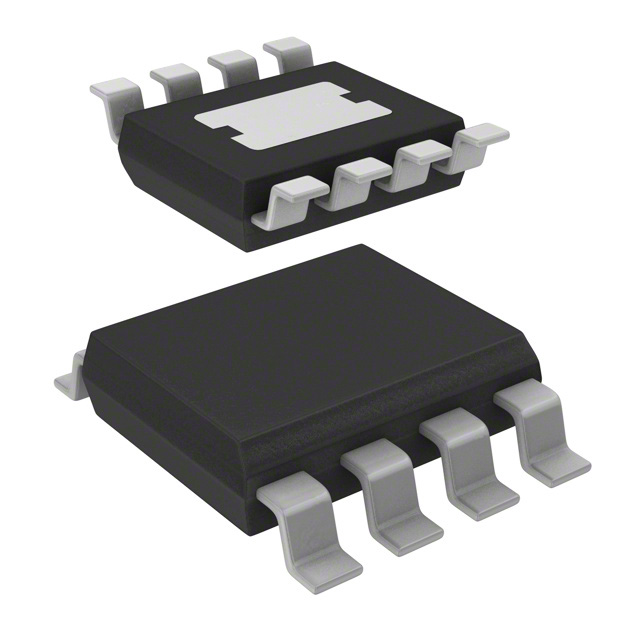
n Available in Thermally Enhanced SOIC-8E or
TSSOP-16E Packages
The LTC®6090/LTC6090-5 are high voltage, precision
monolithic operational amplifiers. The LTC6090 is unity
gain stable. The LTC6090-5 is stable in noise gain configurations of 5 or greater. Both amplifiers feature high
open loop gain, low input referred offset voltage and noise,
and pA input bias current and are ideal for high voltage,
high impedance buffering and/or high gain configurations.
n
The amplifiers are internally protected against overtemperature conditions. A thermal warning output, TFLAG,
goes active when the die temperature approaches 150°C.
The output stage may be turned off with the output disable
pin OD. By tying the OD pin to the thermal warning output
(TFLAG), the part will disable the output stage when it is
out of the safe operating area. These pins easily interface
to any logic family.
APPLICATIONS
n
n
n
n
n
Both amplifiers may be run from a single 140V or spit
±70V power supplies and are capable of driving up to
200pF of load capacitance. They are available in either an
8-lead SO or 16-lead TSSOP package with exposed pad
for low thermal resistance.
ATE
Piezo Drivers
Photodiode Amplifier
High Voltage Regulators
Optical Networking
L, LT, LTC, LTM, Linear Technology and the Linear logo are registered trademarks of Linear
Technology Corporation. All other trademarks are the property of their respective owners.
TYPICAL APPLICATION
High Voltage DAC Buffer Application
140VP-P Sine Wave Output
80
3V
DIN
16
LTC2641
10k
+
470pF
LTC6090
VOUT = ±70V
–
VREF
2.5V
16.2k
OUTPUT VOLTAGE (V)
60
70V
40
20
0
–20
–40
–60
–70V
–80
453k
6090 TA01a
25µs/DIV
6090 TA01b
16.9k
10pF
6090fe
For more information www.linear.com/LTC6090
1
�LTC6090/LTC6090-5
ABSOLUTE MAXIMUM RATINGS
(Note 1)
Total Supply Voltage (V+ to V–)................................150V
COM.................................................................... V– to V+
Input Voltage
OD....................................................... V– to V+ + 0.3V
+IN, –IN,................................... V– – 0.3V to V+ + 0.3V
OD to COM................................................... –3V to 7V
Input Current
+IN, –IN............................................................ ±10mA
TFLAG Output
TFLAG.......................................V – – 0.3V to V+ + 0.3V
TFLAG to COM............................................. –3V to 7V
Output Current
Continuous (Note 2).................................... 50mARMS
Operating Junction Temperature Range
(Note 3)....................................................–40°C to 125°C
Specified Junction Temperature Range (Note 4)
LTC6090C................................................. 0°C to 70°C
LTC6090I..............................................–40°C to 85°C
LTC6090H........................................... –40°C to 125°C
Junction Temperature (Note 5).............................. 150°C
Storage Temperature Range................... –65°C to 150°C
Lead Temperature (Soldering, 10 sec).................... 300°C
PIN CONFIGURATION
TOP VIEW
TOP VIEW
COM 1
–IN 2
+IN 3
V–
9
V–
4
COM
1
16 OD
GUARD
2
15 GUARD
14 V+
8
OD
GUARD
3
7
V+
–IN
4
6
OUT
+IN
5
GUARD
6
11 GUARD
GUARD
7
10 GUARD
V–
8
9
5
TFLAG
S8E PACKAGE
8-LEAD PLASTIC SO
TJMAX = 150°C, θJC = 5°C/W
EXPOSED PAD (PIN 9) IS V–, MUST BE SOLDERED TO PCB
17
V–
13 GUARD
12 OUT
TFLAG
FE PACKAGE
16-LEAD PLASTIC TSSOP
TJMAX = 150°C, θJC = 10°C/W
EXPOSED PAD (PIN 17) IS V–, MUST BE SOLDERED TO PCB
ORDER INFORMATION
LEAD FREE FINISH
TAPE AND REEL
PART MARKING*
PACKAGE DESCRIPTION
JUNCTION TEMPERATURE RANGE
LTC6090CS8E#PBF
LTC6090CS8E#TRPBF
6090
8-Lead Plastic SO
0°C to 70°C
LTC6090IS8E#PBF
LTC6090IS8E#TRPBF
6090
8-Lead Plastic SO
–40°C to 85°C
LTC6090HS8E#PBF
LTC6090HS8E#TRPBF
6090
8-Lead Plastic SO
–40°C to 125°C
LTC6090CFE#PBF
LTC6090CFE#TRPBF
6090FE
16-Lead Plastic TSSOP
0°C to 70°C
LTC6090IFE#PBF
LTC6090IFE#TRPBF
6090FE
16-Lead Plastic TSSOP
–40°C to 85°C
LTC6090HFE#PBF
LTC6090HFE#TRPBF
6090FE
16-Lead Plastic TSSOP
–40°C to 125°C
2
6090fe
For more information www.linear.com/LTC6090
�LTC6090/LTC6090-5
ORDER INFORMATION
LEAD FREE FINISH
TAPE AND REEL
PART MARKING*
PACKAGE DESCRIPTION
JUNCTION TEMPERATURE RANGE
LTC6090CS8E-5#PBF
LTC6090CS8E-5#TRPBF
60905
8-Lead Plastic SO
0°C to 70°C
LTC6090IS8E-5#PBF
LTC6090IS8E-5#TRPBF
60905
8-Lead Plastic SO
–40°C to 85°C
LTC6090HS8E-5#PBF
LTC6090HS8E-5#TRPBF
60905
8-Lead Plastic SO
–40°C to 125°C
LTC6090CFE-5#PBF
LTC6090CFE-5#TRPBF
6090FE-5
16-Lead Plastic TSSOP
0°C to 70°C
LTC6090IFE-5#PBF
LTC6090IFE-5#TRPBF
6090FE-5
16-Lead Plastic TSSOP
–40°C to 85°C
LTC6090HFE-5#PBF
LTC6090HFE-5#TRPBF
6090FE-5
16-Lead Plastic TSSOP
–40°C to 125°C
Consult LTC Marketing for parts specified with wider operating temperature ranges. *The temperature grade is identified by a label on the shipping container.
For more information on lead free part marking, go to: http://www.linear.com/leadfree/
For more information on tape and reel specifications, go to: http://www.linear.com/tapeandreel/. Some packages are available in 500 unit reels through
designated sales channels with #TRMPBF suffix.
ELECTRICAL
CHARACTERISTICS
The l denotes the specifications which apply over the full operating
temperature range, otherwise specifications and all typical values are at TJ = 25°C. Test conditions are V+ = 70V, V– = –70V, VCM =
VOUT = 0V, VOD = Open unless otherwise noted.
C-, I-SUFFIXES
SYMBOL PARAMETER
VOS
CONDITIONS
MIN
Input Offset Voltage
l
∆VOS /∆T Input Offset Voltage Drift
TA = 25°C, ∆TJ = 70°C
IB
Input Bias Current (Note 6)
Supply Voltage = ±70V
Supply Voltage = ±15V
Supply Voltage = ±15V
IOS
Input Offset Current (Note 6)
Supply Voltage = ±15V
–5
MAX
±330
±330
±1000
±1250
±3
5
3
0.3
l
0.5
l
en
H-SUFFIX
TYP
MIN
–5
TYP
MAX
UNITS
±330
±330
±1000
±1250
μV
μV
±3
5
3
0.3
50
0.5
30
µV/°C
800
pA
pA
pA
120
pA
pA
Input Noise Voltage Density
f = 1kHz
f = 10kHz
14
11
14
11
Input Noise Voltage
0.1Hz to 10Hz
3.5
3.5
µVP-P
1
1
fA/√Hz
in
Input Noise Current Density
VCM
Input Common Mode Range
Guaranteed by CMRR
l
V –+3V
±68
V+ –3V
V –+3V
±68
nV/√Hz
nV/√Hz
V+ –3V
V
V
CIN
Common Mode Input
Capacitance
9
9
pF
CDIFF
Differential Input Capacitance
5
5
pF
CMRR
Common Mode Rejection Ratio VCM = –67V to 67V
PSRR
VOUT
AVOL
Power Supply Rejection Ratio
130
126
>140
130
126
>140
l
dB
dB
112
106
>120
112
106
>120
l
dB
dB
VS = ±4.75V to ±70V
Output Voltage Swing High (VOH) No Load
(Referred to V+)
ISOURCE = 1mA
ISOURCE = 10mA
l
l
l
10
50
450
25
140
1000
10
50
450
25
140
1000
mV
mV
mV
Output Voltage Swing Low (VOL) No Load
(Referred to V –)
ISINK = 1mA
ISINK = 10mA
l
l
l
10
40
250
25
80
600
10
40
250
25
80
600
mV
mV
mV
Large-Signal Voltage Gain
RL = 10k,
VOUT from –60V to 60V
l
1000
1000
>10000
1000
1000
>10000
V/mV
V/mV
6090fe
For more information www.linear.com/LTC6090
3
�LTC6090/LTC6090-5
ELECTRICAL
CHARACTERISTICS
The l denotes the specifications which apply over the full operating
temperature range, otherwise specifications and all typical values are at TJ = 25°C. Test conditions are V+ = 70V, V– = –70V, VCM =
VOUT = 0V, VOD = Open unless otherwise noted.
C-, I-SUFFIXES
SYMBOL PARAMETER
ISC
SR
GBW
CONDITIONS
MIN
TYP
Output Short-Circuit Current
(Source and Sink)
Supply Voltage = ±70V
Supply Voltage = ±15V
l
50
Slew Rate
AV = –4, RL = 10k
LTC6090
LTC6090-5
l
l
10
18
21
37
fTEST = 20kHz, RL = 10k
LTC6090
LTC6090-5
l
l
5.5
11
12
24
Gain-Bandwidth Product
ΦM
Phase Margin
RL = 10k, CL = 50pF
FPBW
Full Power Bandwidth
VO = 125VP–P
LTC6090
LTC6090-5
tS
Settling Time 0.1%
∆VOUT = 1V
LTC6090, AV = 1V/V
LTC6090-5, AV = 5V/V
IS
Supply Current
No Load
H-SUFFIX
MAX
90
MIN
20
34
40
68
2.8
VS
Supply Voltage Range
Guaranteed by the PSRR Test l
ODH
ODL
OD Pin Voltage, Referenced to
COM Pin
VIH
VIL
Amplifier DC Output
Impedance, Disabled
DC, OD = COM
9.5
9
16
21
37
V/μs
V/μs
5
10
12
24
MHz
MHz
60
Deg
40
68
kHz
kHz
2
2.5
µs
µs
18
32
3.9
4.3
140
l COM+1.8V
l
COM+0.65V
2.8
9.5
COM+1.8V
>10
V–
3.9
4.3
mA
mA
140
V
COM+0.65V
V
V
>10
V+ – 5
UNITS
mA
mA
2
2.5
l
MAX
90
50
60
l
l
TYP
V–
MΩ
V+ – 5
COMCM
COM Pin Voltage Range
l
17
21
25
17
21
25
V
500
665
850
500
665
850
kΩ
COMV
COM Pin Open Circuit Voltage
l
COMR
COM Pin Resistance
l
TEMPF
Die Temperature Where TFLAG
Is Active
TEMPHYS TFLAG Output Hysteresis
ITFLAG
TFLAG Pull-Down Current
TFLAG Output Voltage = 0V
Note 1: Stresses beyond those listed under Absolute Maximum Ratings
may cause permanent damage to the device. Exposure to any Absolute
Maximum Rating condition for extended periods may affect device
reliability and lifetime.
Note 2: The LTC6090/LTC6090-5 is capable of producing peak output
currents in excess of 50mA. Current density limitations within the IC require
the continuous RMS current supplied by the output (sourcing or sinking)
over the operating lifetime of the part be limited to under 50mA (Absolute
Maximum). Proper heat sinking may be required to keep the junction
temperature below the absolute maximum rating. Refer to Figure 7, the
Power Dissipation section, and the Safe Operating Area section of the data
sheet for more information.
Note 3: The LTC6090C/LTC6090I are guaranteed functional over the
operating junction temperature range –40°C to 85°C. The LTC6090H
is guaranteed functional over the operating junction temperature range
–40°C to 125°C. Specifying the junction temperature range as an operating
condition is applicable for devices with potentially significant quiescent
power dissipation.
4
l
70
V
145
145
°C
5
5
°C
200
330
70
200
330
µA
Note 4: The LTC6090C is guaranteed to meet specified performance from
0°C to 70°C. The LTC6090C is designed, characterized, and expected
to meet specified performance from –40°C to 85°C but is not tested or
QA sampled at these temperatures. The LTC6090I is guaranteed to meet
specified performance from –40°C to 85°C. The LTC6090H is guaranteed
to meet specified performance from –40°C to 125°C.
Note 5: This device includes over temperature protection that is intended
to protect the device during momentary overload conditions. Operation
above the specified maximum operating junction temperature is not
recommended.
Note 6: Input bias and offset current is production tested with ±15V
supplies. See Typical Performance Characteristics curves of actual typical
performance over full supply range.
6090fe
For more information www.linear.com/LTC6090
�LTC6090/LTC6090-5
TYPICAL PERFORMANCE CHARACTERISTICS
Open Loop Gain and Phase
vs Frequency
CMRR vs Frequency
100
100
80
PHASE
60
60
40
40
20
20
–20
0.1
1
–40
10000
10
100
1000
FREQUENCY (kHz)
LTC6090
60
0
0.1
1
10
100
FREQUENCY (kHz)
60
200
150
100
40
50
20
–500
0
500
VOS (µV)
0
1000
500
200
100
0
–100
4
300
200
0
–300
–400
–400
50
25
0
75
TEMPERATURE (°C)
100
125
6090 G07
–500
5
125°C
85°C
25°C
–50°C
–50
–25
0
25
50
INPUT COMMON MODE VOLTAGE (V)
75
6090 G06
Minimum Supply Voltage
100
–300
VS = ±70V
–10
6090 G05
–200
–25
0
–20
–75
6
–100
–200
–500
–50
–2
0
2
TCVOS (µV/°C)
TA = 25°C
5 SAMPLES
V+ = – V –
VCM = 0V
400
OFFSET VOLTAGE (µV)
300
–4
SPECIFIED COMMON
MODE RANGE= ±67V
10
Offset Voltage
vs Total Supply Voltage
VS = ±70V
VCM = 0V
5 SAMPLES
400
–6
6090 G04
Offset Voltage vs Temperature
VOLTAGE OFFSET (µV)
CHANGE IN OFFSET VOLTAGE (µV)
80
1000
20
VS = ±70V
T = 25°C
300 A
∆TJ = 70°C
VCM = 0V
250
NUMBER OF UNITS
NUMBER OF UNITS
100
10
100
FREQUENCY (kHz)
Change in Offset Voltage
vs Input Common Mode Voltage
350
VS = ±70V
180 TA = 25°C
V = 0V
160 CM
120
1
PSRR–
6090 G03
TCVOS Distribution
200
500
0
0.1
1000
LTC6090-5
LTC6090-5
LTC6090
LTC6090
6090 G02
VOS Distribution
0
–1000
60
20
6090 G01
140
PSRR+
80
40
20
–20
LTC6090
LTC6090-5
100
30
80
105
130
55
TOTAL SUPPLY VOLTAGE (V)
6090 G08
100
CHANGE IN OFFSET VOLTAGE (µV)
0
LTC6090-5
40
0
14
AV = 1V/V
120
80
CMRR (dB)
GAIN
PSRR vs Frequency
140
VS = ±70V
100
PHASE (DEG)
GAIN (dB)
80
120
PSRR (dB)
120
75
50
25
0
–25
–50
125°C
85°C
25°C
–50°C
–75
–100
5
6
7
9
8
TOTAL SUPPLY VOLTAGE (V)
10
6090 G09
6090fe
For more information www.linear.com/LTC6090
5
�LTC6090/LTC6090-5
TYPICAL PERFORMANCE CHARACTERISTICS
Supply Current
vs Total Supply Voltage
3.0
2.9
2.5
2.8
VS = ±70V
2.7
VS = ±4.75V
2.6
2.5
Output Disable Supply Current
vs Total Supply Voltage
800
OUTPUT DISABLE CURRENT (µA)
3.0
SUPPLY CURRENT (mA)
SUPPLY CURRENT (mA)
Supply Current vs Temperature
2.0
1.5
1.0
0.5
2.4
–50 –25
50
25
75
0
TEMPERATURE (°C)
100
0
125
TA = 25°C
0
25
50
75
100
SUPPLY VOLTAGE (V)
125
6090 G10
10
10
15
150
100
50
10
100
1000
FREQUENCY (kHz)
100
1000
FREQUENCY (kHz)
10000
LTC6090-5 Small Signal
Frequency Response
vs Closed Loop Gain
30
GAIN (dB)
GAIN (dB)
GAIN (dB)
10
40
10
–10
10000
1
50
20
–5
6090 G16
6
5
–5
10000
40
0
100
1000
FREQUENCY (kHz)
10
6090 G15
0
10
RF = 40.2k
RI = 10k
CF = 2pF
0
30
1
LTC6090
LTC6090-5
6090 G14
15
–10
50
75
100
125
25
TOTAL SUPPLY VOLTAGE (V)
Small Signal Frequency Response
50
5
0
6090 G12
LTC6090 Small Signal Frequency
Response vs Closed Loop Gain
RF = 40.2k
RI = 10k
125°C
85°C
25°C
–50°C
100
200
0
100
CF = 0pF
CF = 1pF
CF = 2pF
10
200
20
LTC6090-5 Small Signal
Frequency Response
vs Feedback Capacitance
20
300
250
6090 G13
25
400
0
150
GAIN (dB)
INTEGRATED NOISE (µVRMS)
VOLTAGE NOISE DENSITY (nV/√Hz)
100
0.1
1
FREQUENCY (kHz)
500
Integrated Noise vs Frequency
1000
0.010
600
6090 G11
Voltage Noise Density
vs Frequency
1
0.001
700
–20
20
10
AV = 101V/V
AV = 11V/V
AV = 1V/V
1
10
100
1000
FREQUENCY (kHz)
101V/V
33V/V
11V/V
5V/V
0
10000
6090 G17
–10
1
10
100
1000
FREQUENCY (kHz)
10000
6090 G18
6090fe
For more information www.linear.com/LTC6090
�LTC6090/LTC6090-5
TYPICAL PERFORMANCE CHARACTERISTICS
1000
10
1
0.01
AV = 101V/V
AV = 11V/V
AV = 1V/V
1
10
1000
100
10
1
100
1000 10000 100000
FREQUENCY (kHz)
1
10
100
FREQUENCY (kHz)
60
DIRECTION OF THE CURRENT
IS OUT OF THE PIN
50°C
25°C
0.1
–15
–10
–5
0
10
5
COMMON MODE VOLTAGE (V)
15
100°C
80°C
DIRECTION OF THE CURRENT
IS OUT OF THE PIN
50°C
25°C
LTC6090-5 Large Signal Transient
Response
80
AV = –10V/V
VS = ±70V
OUTPUT
60
40
20
0
INPUT
–20
0
INPUT
–20
–60
–60
–80
6090 G23
AV = –10V/V
VS = ±70V
RF = 100kΩ
RI = 10kΩ
CF = 2pF
20
–40
5µs/DIV
OUTPUT
40
–40
–80
80
6090 G21
OUTPUT, INPUT (V)
85°C
1
80
VS = ±15V
100°C
10
1
LTC6090 Large Signal Transient
Response
OUTPUT, INPUT (V)
INPUT BIAS CURRENT (|pA|)
100
10
125°C
6091 G20
Input Bias Current vs Common
Mode Voltage and Temperature
125°C
100
VS = ±70V
5°C
0.1
20 40 60
–80 –60 –40 –20 0
COMMON MODE VOLTAGE (V)
1000
6090 G19
1000
10000
CL = 10pF
INPUT BIAS CURRENT (|pA|)
100
OUTPUT IMPEDANCE (kΩ)
OUTPUT IMPEDACNE (Ω)
1000
0.1
Input Bias Current vs Common
Mode Voltage and Temperature
Output Impedance vs Frequency
with Output Disabled (OD = COM)
Output Impedance vs Frequency
6090 G24
5µs/DIV
6090 G22
LTC6090 Falling Edge
Settling Time
Small Signal Transient Response
AV = 1V/V
LTC6090 Rising Edge
Settling Time
6090 G16
500ns/DIV
6090 G26
INPUT STEP (0.5V/DIV)
INPUT STEP (0.5V/DIV)
1µs/DIV
INPUT
OUTPUT STEP (20mV/DIV)
OUTPUT
50mV/DIV
OUTPUT STEP (20mV/DIV)
OUTPUT
INPUT
50mV/DIV
AV = 1V/V
AV = 1V/V
OUTPUT
INPUT
500ns/DIV
6090 G27
6090fe
For more information www.linear.com/LTC6090
7
�LTC6090/LTC6090-5
TYPICAL PERFORMANCE CHARACTERISTICS
LTC6090-5 Rising Edge
Settling Time
LTC6090-5 Small Signal
Transient Response
LTC6090-5 Falling Edge
Settling Time
INPUT (100mV/DIV)
INPUT (100mV/DIV)
INPUT
AV = 5V/V
RF = 40.2kΩ
RI = 10kΩ
CF = 2pF
OUTPUT
6090 G28
1µs/DIV
OUTPUT (50mV/DIV)
OUTPUT
100mV/DIV
OUTPUT (50mV/DIV)
INPUT
25mV/DIV
INPUT
OUTPUT
AV = 5V/V
RF = 40.2kΩ
RI = 10kΩ
CF = 2pF
AV = 5V/V
RF = 40.2kΩ
RI = 10kΩ
CF = 2pF
6090 G29
500ns/DIV
500ns/DIV
6090 G30
Output Disable (OD) Response
Time
OD-COM
OUTPUT
ENABLED
0.1Hz to 10Hz Voltage Noise
160
AV = –10V/V
VIN = –0.5V
AV = –10V/V
VS = ±70V
RF = 100kΩ
RI = 10kΩ
CF = 2pF
140
120
OUTPUT
DISABLED
VOUT (VP-P)
2V/DIV
OD-COM
= 0V
Output Voltage Swing
vs Frequency
VOUT
VOUT
= 0V
100
OUTPUT
NOISE
2µV/DIV
80
60
40
20
20µs/DIV
0
6090 G31
LTC6090
LTC6090-5
1
10
100
FREQUENCY (kHz)
1000
6090 G33
TIME (1s/DIV)
6090 G32
SUPPLY CURRENT (mA)
2.5
2.0
1.5
1.0
125°C
85°C
25°C
–50°C
0.5
0
75
VS = ±70V
VCOM = 0V
0.5
0.8
1.0
1.3
1.5
OD-COM (V)
1.8
2.0
OD INPUT CURRENT (µA)
3.0
OD Pin Input Current
vs OD Pin Voltage
Output Voltage Swing High (VOH)
vs Load Current and Temperature
50
125°C
85°C
25°C
–50°C
700
600
25
0
500
400
300
200
–25
100
–50
0
1
2
3
4
OD-COM (V)
5
7
6
6090 G35
6090 G34
8
800
125°C
85°C
25°C
–50°C
VS = ±70V
VCOM = 0V
VOH (mV)
Supply Current vs OD Pin Voltage
0
0
2
4
6
ISOURCE (mA)
8
10
6090 G36
6090fe
For more information www.linear.com/LTC6090
�LTC6090/LTC6090-5
TYPICAL PERFORMANCE CHARACTERISTICS
Output Voltage Swing Low (VOL)
vs Load Current and Temperature
LTC6090 Distortion vs Frequency
–20
125°C
85°C
25°C
–50°C
450
400
–40
DISTORTION (dBc)
VOL (mV)
300
250
200
150
–50
–70
–90
–100
–110
2
4
6
ISOURCE (mA)
8
–120
10
2ND
–80
50
0
2.5
–60
100
0
VS = ±70V
AV = 10
VOUT = 10VP-P
RL = 10k
–30
350
Thermal Shutdown Hysteresis
3.0
SUPPLY CURRENT (mA)
500
3RD
2.0
1.5
1.0
0.5
10
0
162 164 166 168 170 172 174 176 178
JUNCTION TEMPERATURE (°C)
100
FREQUENCY (kHz)
6090 G38
6090 G39
6090 G37
Open Circuit Voltage of COM,
OD, TFLAG
CHANGE IN VOLTAGE OFFSET (µV)
80
PIN VOLTAGE (V)
40
OD
COM
TFLAG
–
V = 0V
60
40
20
0
0
20
40
60
80 100 120
TOTAL SUPPLY VOLTAGE (V)
140
6090 G40
40
VS = ±70V
RLOAD = 10k
TA = 25°C
10 SAMPLES
30
20
CHANGE IN VOLTAGE OFFSET (µV)
100
Open Loop Gain
vs Load Resistance
Open Loop Gain
10
0
–10
–20
–30
–40
–70
–50
–25
0
25
OUTPUT VOLTAGE (V)
50
75
6090 G41
RLOAD = 500k
RLOAD = 10k
RLOAD = 100k
30
20
10
0
–10
–20
–30
–40
–70
–50
–25
0
25
OUTPUT VOLTAGE (V)
50
75
6090 G42
6090fe
For more information www.linear.com/LTC6090
9
�LTC6090/LTC6090-5
PIN FUNCTIONS
(S8E/FE)
COM (Pin 1/Pin 1): COM Pin is used to interface OD and
TFLAG pins to voltage control circuits. Tie this pin to the
low voltage ground, or let it float.
–IN (Pin 2/Pin 4): Inverting Input Pin. Input common
mode range is V – + 3V to V + – 3V. Do not exceed absolute
maximum voltage range.
+IN (Pin 3/Pin 5): Noninverting Input Pin. Input common
mode range is V – + 3V to V + – 3V. Do not exceed absolute
maximum voltage range.
V– (Pin 4, Exposed Pad Pin 9/Pin 8, Exposed Pad
Pin 17): Negative Supply Pin. Connect to V– Only. To
achieve low thermal resistance connect this pin to the
V – power plane. The V – power plane connection removes
heat from the device and should be electrically isolated
from all other power planes.
OUT (Pin 6/Pin 12): Output Pin. If this rail-to-rail output
goes below V– , the ESD protection diode will forward
bias. If OUT goes above V+, then output device diodes
will forward bias. Avoid forward biasing the diodes on the
OUT pin. Excessive current can cause damage.
V+ (Pin 7/Pin 14): Positive Supply Pin.
OD (Pin 8/Pin 16): Output Disable Pin. Active low input
disables the output stage. If left open, an internal pull-up
resistor enables the amplifier. Input voltage levels are
referred to the COM pin.
GUARD (NA/Pins 2, 3, 6, 7, 10, 11, 13, 15): Guard pins
increase clearance and creepage between other pins.
Pins 3 and 6 can be used to build guard rings around the
inputs.
TFLAG (Pins 5, 9/Pins 9, 17): Temperature Flag Pin. The
TFLAG pin is an open drain output that sinks current when
the die temperature exceeds 145°C.
10
6090fe
For more information www.linear.com/LTC6090
�LTC6090/LTC6090-5
BLOCK DIAGRAM
V+
V+
2M
2M
10k
COM
10k
OD
1.2V
2M
–
ESD
+
ESD
V–
V
–
V+
125Ω
–IN
ESD
V+
ESD
+IN
V–
OUTPUT
ENABLE
DIFFERENTIAL
DRIVE
GENERATOR
125Ω
OUT
ESD
V–
TO COM PIN
6k
500Ω
V–
INPUT STAGE
6k
TJ > 175°C
DIE
TEMPERATURE
TJ > 145°C
SENSOR
TFLAG
ESD
V–
V–
6090 BD
6090fe
For more information www.linear.com/LTC6090
11
�LTC6090/LTC6090-5
APPLICATIONS INFORMATION
General
The LTC6090 high voltage operational amplifier is designed
in a Linear Technology proprietary process enabling a railto-rail output stage with a 140V supply while maintaining
precision, low offset, and low noise.
Power Supply
The LTC6090 works off single or split supplies. Split supplies can be balanced or unbalanced. For example, two
±70V supplies can be used, or a 100V and –40V supply
can be used. For single supply applications place a high
quality surface mount ceramic 0.1µF bypass capacitor
between the supply pins close to the part. For dual supply
applications use two high quality surface mount ceramic
capacitors between V+ to ground, and V– to ground located
close to the part. When using split supplies, supply sequencing does not cause problems.
Input Protection
As shown in the block diagram, the LTC6090 has a comprehensive protection network to prevent damage to the
input devices. The current limiting resistors and back to
back diodes are to keep the inputs from being driven apart.
The voltage-current relationship combines exponential
and resistive until the voltage difference between the pins
reach 12V.
At that point the Zeners turn on. Additional current into
the pins will snap back the input differential voltage to 9V.
In the event of an ESD strike between an input and V–, the
voltage clamps and ESD device fire providing a current
path to V– protecting the input devices.
The input pin protection is designed to protect against
momentary ESD events. A repetitive large fast input swing
(>5.5V and