LTC6431-20
20dB Gain Block,
50Ω IF Amplifier
FEATURES
DESCRIPTION
50Ω Matched 20MHz to 1400MHz
n 20.8dB Power Gain
n 46.2dBm OIP3 at 240MHz Into 50Ω
n NF = 2.6dB at 240MHz
n 0.6nV/√Hz Total Input Noise
n S11 < –10dB Up to 2.0GHz
n S22 < –10dB Up to 1.4GHz
n >2.0V
P-P Linear Output Swing
n P1dB = 22.0dBm
n 50Ω Single-Ended Input/Output
n Insensitive to V
CC Variation
n A-Grade 100% OIP3 Tested at 240MHz
n Input/Output Internally Matched to 50Ω
n Single 5V Supply
The LTC®6431-20 is a gain block amplifier exhibiting
excellent linearity at frequencies beyond 1000MHz and
with low associated output noise.
n
The unique combination of linearity, low noise and low
power dissipation make this an ideal candidate for many
signal-chain applications. The LTC6431-20 is easy to
use, requiring a minimum of external components. It is
internally input/output matched to 50Ω and it draws only
93mA from a single 5V supply.
On-chip bias and temperature compensation maintain
performance over environmental changes.
The LTC6431-20 uses a high performance SiGe BiCMOS
process for excellent repeatability compared with similar
GaAs amplifiers. All A-grade LTC6431-20 devices are tested
and guaranteed for OIP3 at 240MHz. The LTC6431-20 is
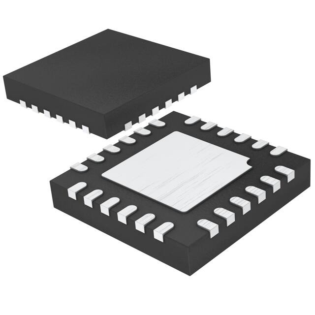
housed in a 4mm × 4mm 24-lead QFN package with an
exposed pad for thermal management and low inductance.
APPLICATIONS
Single-Ended IF Amplifier
ADC Driver
n CATV
n
n
LTC6431 FAMILY
GAIN
LTC6431-15
15.5dB
LTC6431-20
20.8dB
L, LT, LTC, LTM, Linear Technology and the Linear logo are registered trademarks of Linear
Technology Corporation. All other trademarks are the property of their respective owners.
TYPICAL APPLICATION
OIP3 vs Frequency
Single-Ended IF Amplifier
VCC = 5V
52
50
5V
48
OIP3 (dBm)
RF CHOKE
560nH
LTC6431-20
50Ω
1000pF
1000pF
50Ω
643120 TA01a
46
44
42
VCC = 5V
TA = 25°C
POUT = 2dBm/TONE
38 fSPACE = 1MHz
ZIN = ZOUT = 50Ω
36
200
400
0
40
600
FREQUENCY (MHz)
800
1000
643120 TA01b
643120f
For more information www.linear.com/LTC6431-20
1
�LTC6431-20
PIN CONFIGURATION
Total Supply Voltage (VCC to GND)...........................5.5V
Amplifier Output Current (+OUT)..........................120mA
RF Input Power, Continuous, 50Ω (Note 2)..........15dBm
RF Input Power, 100µs Pulse, 50Ω (Note 2).........20dBm
Operating Case Temperature Range
(TCASE)......................................................–40°C to 85°C
Storage Temperature Range................... –65°C to 150°C
Junction Temperature (TJ)..................................... 150°C
DNC
DNC
DNC
VCC
GND
IN
TOP VIEW
24 23 22 21 20 19
DNC 1
18 OUT
DNC 2
17 GND
DNC 3
16 T_DIODE
25
GND
DNC 4
15 DNC
DNC 5
14 DNC
DNC 6
13 DNC
DNC
DNC
9 10 11 12
DNC
8
VCC
7
DNC
(Note 1)
GND
ABSOLUTE MAXIMUM RATINGS
UF PACKAGE
24-LEAD (4mm × 4mm) PLASTIC QFN
TJMAX = 150°C, θJC = 54°C/W
EXPOSED PAD (PIN 25) IS GND, MUST BE SOLDERED TO PCB
ORDER INFORMATION
LEAD FREE FINISH
TAPE AND REEL
PART MARKING*
PACKAGE DESCRIPTION
TEMPERATURE RANGE
LTC6431AIUF-20#PBF
LTC6431AIUF-20#TRPBF
43120
24-Lead (4mm × 4mm) Plastic QFN
–40°C to 85°C TCASE
LTC6431BIUF-20#PBF
LTC6431BIUF-20#TRPBF
43120
24-Lead (4mm × 4mm) Plastic QFN
–40°C to 85°C TCASE
Consult LTC Marketing for parts specified with wider operating temperature ranges. *The temperature grade is identified by a label on the shipping container.
Consult LTC Marketing for information on nonstandard lead based finish parts.
For more information on lead free part marking, go to: http://www.linear.com/leadfree/
For more information on tape and reel specifications, go to: http://www.linear.com/tapeandreel/
DC ELECTRICAL CHARACTERISTICS
The l denotes the specifications which apply over the full operating
temperature range, otherwise specifications are at TA = 25°C. VCC = 5V, ZSOURCE = ZLOAD = 50Ω. Typical measured DC electrical
performance using Test Circuit A.
SYMBOL
PARAMETER
VS
Operating Supply Range
IS(TOT)
Total Supply Current
IS(OUT)
ICC
Total Supply Current to OUT Pin
Current to VCC Pin
CONDITIONS
MIN
TYP
MAX
UNITS
l
4.75
5.0
5.25
V
75
68
93
l
113
129
mA
mA
55
51
75
l
95
115
mA
mA
15
12.5
18
l
21
21.5
mA
mA
All VCC Pins Plus OUT
Current to OUT
Either VCC Pin May Be Used
643120f
2
For more information www.linear.com/LTC6431-20
�LTC6431-20
AC ELECTRICAL CHARACTERISTICS
The l denotes the specifications which apply over the full operating
temperature range, otherwise specifications are at TA = 25°C (Note 3). VCC = 5V, ZSOURCE = ZLOAD = 50Ω unless otherwise noted.
Measurements are performed using Test Circuit A, measuring from 50Ω SMA to 50Ω without de-embedding (Note 4).
SYMBOL
PARAMETER
CONDITIONS
–3dB Bandwidth
De-embedded to Package
(Low Frequency Cutoff = 20MHz)
MIN
TYP
MAX
UNITS
Small Signal
BW
2000
MHz
S11
Input Return Loss 20MHz to 2000MHz
De-embedded to Package
–10
dB
S21
Forward Power Gain 50MHz to 1000MHz
De-embedded to Package
20.8
dB
S12
Reverse Isolation 20MHz to 3000MHz
De-embedded to Package
–23
dB
S22
Output Return Loss 20MHz to 1400MHz
De-embedded to Package
–10
dB
Frequency = 50MHz
S21
Power Gain
De-embedded to Package
21.1
dB
OIP3
Output Third-Order Intercept Point
POUT = 2dBm/Tone, ∆f = 1MHz, A-Grade
POUT = 2dBm/Tone, ∆f = 1MHz, B-Grade
48.2
47.2
dBm
dBm
IM3
Third-Order Intermodulation
POUT = 2dBm/Tone, ∆f = 1MHz, A-Grade
POUT = 2dBm/Tone, ∆f = 1MHz, B-Grade
–92.4
–90.4
dBc
dBc
dBc
HD2
Second Harmonic Distortion
POUT = 6dBm
–53.5
HD3
Third Harmonic Distortion
POUT = 6dBm
–93.6
dBc
P1dB
Output 1dB Compression Point
23.5
dBm
NF
Noise Figure
De-embedded to Package
2.6
dB
Frequency = 140MHz
S21
Power Gain
De-embedded to Package
21.0
dB
OIP3
Output Third-Order Intercept Point
POUT = 2dBm/Tone, ∆f = 1MHz, A-Grade
POUT = 2dBm/Tone, ∆f = 1MHz, B-Grade
48.8
47.8
dBm
dBm
IM3
Third-Order Intermodulation
POUT = 2dBm/Tone, ∆f = 1MHz, A-Grade
POUT = 2dBm/Tone, ∆f = 1MHz, B-Grade
–93.6
–91.6
dBc
dBc
HD2
Second Harmonic Distortion
POUT = 6dBm
–55.8
dBc
HD3
Third Harmonic Distortion
POUT = 6dBm
–96.6
dBc
23.0
dBm
2.7
dB
P1dB
Output 1dB Compression Point
NF
Noise Figure
De-embedded to Package
Frequency = 240MHz
S21
Power Gain
De-embedded to Package
l
19.4
19.0
21.0
42.2
46.2
45.7
OIP3
Output Third-Order Intercept Point
POUT = 2dBm/Tone, ∆f = 1MHz, A-Grade
POUT = 2dBm/Tone, ∆f = 1MHz, B-Grade
IM3
Third-Order Intermodulation
POUT = 2dBm/Tone, ∆f = 1MHz, A-Grade
POUT = 2dBm/Tone, ∆f = 1MHz, B-Grade
–90.4
–87.4
21.4
21.5
dB
dB
dBm
dBm
–80.4
dBc
dBc
HD2
Second Harmonic Distortion
POUT = 6dBm
–50.5
dBc
HD3
Third Harmonic Distortion
POUT = 6dBm
–92.5
dBc
22.0
dBm
2.6
dB
P1dB
Output 1dB Compression Point
NF
Noise Figure
De-embedded to Package
643120f
For more information www.linear.com/LTC6431-20
3
�LTC6431-20
AC ELECTRICAL CHARACTERISTICS
The l denotes the specifications which apply over the full operating
temperature range, otherwise specifications are at TA = 25°C (Note 3). VCC = 5V, ZSOURCE = ZLOAD = 50Ω unless otherwise noted.
Measurements are performed using Test Circuit A, measuring from 50Ω SMA to 50Ω without de-embedding (Note 4).
SYMBOL
PARAMETER
CONDITIONS
MIN
TYP
MAX
UNITS
Frequency = 300 MHz
S21
Power Gain
De-embedded to Package
20.9
dB
OIP3
Output Third-Order Intercept Point
POUT = 2dBm/Tone, ∆f = 1MHz, A-Grade
POUT = 2dBm/Tone, ∆f = 1MHz, B-Grade
45.9
44.8
dBm
dBm
IM3
Third-Order Intermodulation
POUT = 2dBm/Tone, ∆f = 1MHz, A-Grade
POUT = 2dBm/Tone, ∆f = 1MHz, B-Grade
–87.8
–85.6
dBc
dBc
HD2
Second Harmonic Distortion
POUT = 6dBm
–50.5
dBc
HD3
Third Harmonic Distortion
POUT = 6dBm
–83.0
dBc
P1dB
Output 1dB Compression Point
21.8
dBm
NF
Noise Figure
De-embedded to Package
2.7
dB
Frequency = 380MHz
S21
Power Gain
De-embedded to Package
20.9
dB
OIP3
Output Third-Order Intercept Point
POUT = 2dBm/Tone, ∆f = 1MHz, A-Grade
POUT = 2dBm/Tone, ∆f = 1MHz, B-Grade
45.0
44.0
dBm
dBm
IM3
Third-Order Intermodulation
POUT = 2dBm/Tone, ∆f = 1MHz, A-Grade
POUT = 2dBm/Tone, ∆f = 1MHz, B-Grade
–86.0
–84.0
dBc
dBc
HD2
Second Harmonic Distortion
POUT = 6dBm
–50.4
dBc
HD3
Third Harmonic Distortion
POUT = 6dBm
–77.4
dBc
P1dB
Output 1dB Compression Point
NF
Noise Figure
21.7
dBc
De-embedded to Package
2.8
dB
Frequency = 500MHz
S21
Power Gain
De-embedded to Package
20.8
dB
OIP3
Output Third-Order Intercept Point
POUT = 2dBm/Tone, ∆f = 1MHz, A-Grade
POUT = 2dBm/Tone, ∆f = 1MHz, B-Grade
43.9
42.9
dBm
dBm
IM3
Third-Order Intermodulation
POUT = 2dBm/Tone, ∆f = 1MHz, A-Grade
POUT = 2dBm/Tone, ∆f = 1MHz, B-Grade
–83.8
–81.8
dBc
dBc
HD2
Second Harmonic Distortion
POUT = 6dBm
–47.8
dBc
HD3
Third Harmonic Distortion
POUT = 6dBm
–72.6
dBc
P1dB
Output 1dB Compression Point
NF
Noise Figure
21.8
dBm
De-embedded to Package
2.9
dB
Frequency = 600MHz
S21
Power Gain
De-embedded to Package
20.8
dB
OIP3
Output Third-Order Intercept Point
POUT = 2dBm/Tone, ∆f = 1MHz, A-Grade
POUT = 2dBm/Tone, ∆f = 1MHz, B-Grade
41.9
40.9
dBm
dBm
IM3
Third-Order Intermodulation
POUT = 2dBm/Tone, ∆f = 1MHz, A-Grade
POUT = 2dBm/Tone, ∆f = 1MHz, B-Grade
–79.8
–77.8
dBc
dBc
HD2
Second Harmonic Distortion
POUT = 6dBm
–43.7
dBc
HD3
Third Harmonic Distortion
POUT = 6dBm
–64.0
dBc
P1dB
Output 1dB Compression Point
21.6
dBm
NF
Noise Figure
3.0
dB
De-embedded to Package
643120f
4
For more information www.linear.com/LTC6431-20
�LTC6431-20
AC ELECTRICAL CHARACTERISTICS
The l denotes the specifications which apply over the full operating
temperature range, otherwise specifications are at TA = 25°C (Note 3). VCC = 5V, ZSOURCE = ZLOAD = 50Ω unless otherwise noted.
Measurements are performed using Test Circuit A, measuring from 50Ω SMA to 50Ω without de-embedding (Note 4).
SYMBOL
PARAMETER
CONDITIONS
MIN
TYP
MAX
UNITS
Frequency = 700 MHz
S21
Power Gain
De-embedded to Package
20.8
dB
OIP3
Output Third-Order Intercept Point
POUT = 2dBm/Tone, ∆f = 1MHz, A-Grade
POUT = 2dBm/Tone, ∆f = 1MHz, B-Grade
40.7
39.7
dBm
dBm
IM3
Third-Order Intermodulation
POUT = 2dBm/Tone, ∆f = 1MHz, A-Grade
POUT = 2dBm/Tone, ∆f = 1MHz, B-Grade
–77.4
–75.4
dBc
dBc
HD2
Second Harmonic Distortion
POUT = 6dBm
–42.1
dBc
HD3
Third Harmonic Distortion
POUT = 6dBm
–60.7
dBc
P1dB
Output 1dB Compression Point
21.4
dBm
NF
Noise Figure
De-embedded to Package
3.2
dB
Frequency = 800MHz
S21
Power Gain
De-embedded to Package
20.8
dB
OIP3
Output Third-Order Intercept Point
POUT = 2dBm/Tone, ∆f = 1MHz, A-Grade
POUT = 2dBm/Tone, ∆f = 1MHz, B-Grade
39.2
38.2
dBm
dBm
IM3
Third-Order Intermodulation
POUT = 2dBm/Tone, ∆f = 1MHz, A-Grade
POUT = 2dBm/Tone, ∆f = 1MHz, B-Grade
–74.4
–72.4
dBc
dBc
HD2
Second Harmonic Distortion
POUT = 6dBm
–40.5
dBc
HD3
Third Harmonic Distortion
POUT = 6dBm
–63.1
dBc
P1dB
Output 1dB Compression Point
NF
Noise Figure
21.3
dBm
De-embedded to Package
3.4
dB
Frequency = 900MHz
S21
Power Gain
De-embedded to Package
20.8
dB
OIP3
Output Third-Order Intercept Point
POUT = 2dBm/Tone, ∆f = 1MHz, A-Grade
POUT = 2dBm/Tone, ∆f = 1MHz, B-Grade
38.5
37.5
dBm
dBm
IM3
Third-Order Intermodulation
POUT = 2dBm/Tone, ∆f = 1MHz, A-Grade
POUT = 2dBm/Tone, ∆f = 1MHz, B-Grade
–73.0
–71.0
dBc
dBc
HD2
Second Harmonic Distortion
POUT = 6dBm
–37.1
dBc
HD3
Third Harmonic Distortion
POUT = 6dBm
–60.4
dBc
P1dB
Output 1dB Compression Point
NF
Noise Figure
21.1
dBm
De-embedded to Package
3.7
dB
Frequency = 1000MHz
S21
Power Gain
De-embedded to Package
20.8
dB
OIP3
Output Third-Order Intercept Point
POUT = 2dBm/Tone, ∆f = 1MHz, A-Grade
POUT = 2dBm/Tone, ∆f = 1MHz, B-Grade
37.5
36.5
dBm
dBm
IM3
Third-Order Intermodulation
POUT = 2dBm/Tone, ∆f = 1MHz, A-Grade
POUT = 2dBm/Tone, ∆f = 1MHz, B-Grade
–71.0
–69.0
dBc
dBc
HD2
Second Harmonic Distortion
POUT = 6dBm
–36.9
dBc
HD3
Third Harmonic Distortion
POUT = 6dBm
–55.1
dBc
P1dB
Output 1dB Compression Point
20.8
dBc
NF
Noise Figure
3.8
dB
De-embedded to Package
Note 1: Stresses beyond those listed under Absolute Maximum Ratings
may cause permanent damage to the device. Exposure to any Absolute
Maximum Rating condition for extended periods may affect device
reliability and lifetime.
Note 2: Guaranteed by design and characterization. This parameter is not
tested.
Note 3: The LTC6431-20 is guaranteed functional over the case operating
temperature range of –40°C to 85°C.
Note 4: Small-signal parameters S and noise are de-embedded to the
package pins, while large-signal parameters are measured directly from
the circuit.
643120f
For more information www.linear.com/LTC6431-20
5
�LTC6431-20
TYPICAL PERFORMANCE CHARACTERISTICS
TA = 25°C, VCC = 5V, ZSOURCE = ZLOAD = 50Ω unless
otherwise noted. Measurements are performed using Test Circuit A, measuring from 50Ω SMA to 50Ω without de-embedding (Note 4).
Stability Factor K vs Frequency
Over Temperature
S Parameters vs Frequency
25
10
20
9
S21
15
6
0
–5
S22
–10
S11
–15
–20
7
TCASE =
100°C
85°C
70°C
50°C
30°C
0°C
–20°C
–40°C
6
5
4
3
2
–25
S12
–30
0
500
1000 1500 2000
FREQUENCY (MHz)
NOISE FIGURE (dB)
STABILITY FACTOR K
5
MAG (dB)
7
8
10
–35
NF vs Frequency Over Case
Temperature
2500
3000
0
4
3
2
TCASE =
85°C
25°C
–40°C
1
1
0
5
0
4000
2000
1000
3000
FREQUENCY (MHz)
0
400
643120 G02
643120 G01
S11 vs Frequency Over
Temperature
643120 G03
S21 vs Frequency Over
Temperature
0
S12 vs Frequency Over
Temperature
25
0
TCASE =
100°C
85°C
70°C
50°C
30°C
0°C
–20°C
–40°C
–5
20
TCASE =
100°C
85°C
70°C
50°C
30°C
0°C
–20°C
–40°C
–15
–20
–25
0
500
1000 1500 2000
FREQUENCY (MHz)
2500
3000
–10
MAG S12 (dB)
–10
MAG S21 (dB)
MAG S11 (dB)
–5
15
TCASE =
100°C
85°C
10
70°C
50°C
30°C
5
0°C
–20°C
–40°C
0
0
500 1000 1500 2000
FREQUENCY (MHz)
2500
–40
3000
0
500
1000 1500 2000
FREQUENCY (MHz)
2500
3000
643120 G07
6
1000
1500
2000
2500
3000
OIP3 vs Power Out Over
Frequency
54
52
50
48
48
46
46
OIP3 (dBm)
OIP3 (dBm)
MAG S22 (dB)
–25
500
643120 G06
50
TCASE =
100°C
85°C
70°C
50°C
30°C
0°C
–20°C
–40°C
0
FREQUENCY (MHz)
OIP3 vs Frequency
–5
–20
–25
–35
52
–15
–20
643120 G05
0
–10
–15
–30
643120 G04
S22 vs Frequency Over
Temperature
2000
1200
1600
800
FREQUENCY (MHz)
44
42
VCC = 5V
40 TA = 25°C
POUT = 2dBm/TONE
38 fSPACE = 1MHz
ZIN = ZOUT = 50Ω
36
400
200
0
600
FREQUENCY (MHz)
44
42
40
38
36
34
32
800
1000
643120 G08
For more information www.linear.com/LTC6431-20
30
–10 –8 –6 –4 –2 0 2 4 6
RF POWER OUT (dBm/TONE)
50MHz
100MHz
200MHz
240MHz
300MHz
400MHz
500MHz
600MHz
8
10
643120 G09
700MHz
800MHz
900MHz
1000MHz
643120f
�LTC6431-20
TYPICAL PERFORMANCE CHARACTERISTICS
TA = 25°C, VCC = 5V, ZSOURCE = ZLOAD = 50Ω unless
otherwise noted. Measurements are performed using Test Circuit A, measuring from 50Ω SMA to 50Ω without de-embedding (Note 4).
OIP3 vs Frequency Over VCC
Voltage
52
OIP3 vs Tone Spacing Over
Frequency
50
TA = 25°C
POUT = 2dBm/TONE
fSPACE = 1MHz
ZIN = ZOUT = 50Ω
50
48
50
46
45
44
44
42
40
40
38
4.5V
4.75V
5V
5.25V
5.5V
38
36
0
200
OIP3 (dBm)
42
OIP3 (dBm)
OIP3 (dBm)
55
48
46
34
36
34
32
600
400
FREQUENCY (MHz)
30
1000
800
0
643120 G10
HD2 vs Frequency Over POUT
HD3 (dBc)
HD2 (dBc)
–20
–30
–40
RF POUT =
4dBm
6dBm
8dBm
10dBm
–60
10
643120 G12
HD4 vs Input Frequency Over POUT
–10
–10
–20
–20
–30
–30
–40
–40
–50
–60
–70
RF POUT =
4dBm
6dBm
8dBm
10dBm
–90
–100
–110
–60
–70
–90
–100
–110
Total Current vs RF Input Power
100
VCC = 5V
110
95
100
90
90
TOTAL CURRENT (mA)
90
80
ITOT (mA)
70
70
60
50
40
30
60
643120 G16
0
–50
80
75
70
65
55
10
6
85
60
20
4.25 4.5 4.75 5 5.25 5.5 5.75
VCC (V)
0 100 200 300 400 500 600 700 800 900 1000
INPUT FREQUENCY (MHz)
643120 G15
Total Current (ITOT) vs Temperature
TCASE = 25°C
4
–50
–80
0 100 200 300 400 500 600 700 800 900 1000
INPUT FREQUENCY (MHz)
120
80
RF POUT =
4dBm
6dBm
8dBm
10dBm
643120 G14
Total Current (ITOT) vs VCC
ITOT (mA)
700MHz
800MHz
900MHz
1000MHz
0
643120 G13
50
TCASE =
85°C
70°C
50°C
30
VCC = 5V
28°C
POUT = 2dBm/TONE
0°C
25
fSPACE = 1MHz
–20°C
ZIN = ZOUT = 50Ω
–40°C
20
0 100 200 300 400 500 600 700 800 900 1000
FREQUENCY (MHz)
35
0
–80
0 100 200 300 400 500 600 700 800 900 1000
INPUT FREQUENCY (MHz)
100
45 50
643120 G11
HD4 (dBc)
–10
–50
15 20 25 30 35 40
TONE SPACING (MHz)
50MHz
300MHz
100MHz
400MHz
200MHz
500MHz
240MHz
600MHz
5
40
HD3 vs Input Frequency Over POUT
0
–70
OIP3 vs Frequency Over Case
Temperature
–25
0
25
50
TEMPERATURE (°C)
75
100
643120 G17
VSUP = 5V
TA = 25°C
FREQ = 200MHz
50
–15
–10
0
5
–5
RF INPUT POWER (dBm)
10
643120 G18
643120f
For more information www.linear.com/LTC6431-20
7
�LTC6431-20
TYPICAL PERFORMANCE CHARACTERISTICS
TA = 25°C, VCC = 5V, ZSOURCE = ZLOAD = 50Ω unless
otherwise noted. Measurements are performed using Test Circuit A, measuring from 50Ω SMA to 50Ω without de-embedding (Note 4).
Gain vs Output Power
Over Frequency
22
22
21
20
16
14
12
10
8
–10 –8
–6
–4 –2 0
2
4
INPUT POWER (dBm)
6
24
23
20
50MHz
100MHz
200MHz
300MHz
400MHz
500MHz
600MHz
700MHz
800MHz
900MHz
1000MHz
18
18
17
16
8
10
22
50MHz
100MHz
200MHz
300MHz
400MHz
500MHz
600MHz
700MHz
800MHz
900MHz
1000MHz
19
15
P1dB vs Frequency
25
12
P1dB (dBm)
24
GAIN (dB)
OUTPUT POWER (dBm)
Output Power vs Input Power
Over Frequency
20
19
18
17
16
18
16
20
14
OUTPUT POWER (dBm)
22
24
643120 G20
643120 G19
21
15
0
200
600
400
FREQUENCY (MHz)
800
1000
643120 G21
PIN FUNCTIONS
DNC (Pins 1 to 7, 10 to 15, 19 to 21): Do Not Connect.
Do not connect these pins, allow them to float. Failure to
float these pins may impair operation of the LTC6431-20.
T_DIODE (Pin 16): Optional Diode. The T_DIODE can
be forward biased to ground with 1mA of current. The
measured voltage will be an indicator of chip temperature.
GND (Pins 8, 17, 23, Exposed Pad Pin 25): Ground.
For best RF performance, all ground pins should be
connected to the printed circuit board ground plane. The
exposed pad (Pin 25) should have multiple via holes to
an underlying ground plane for low inductance and good
thermal dissipation.
Out (Pin 18): Amplifier Output Pin. A choke inductor is
necessary to provide power from the 5V supply and to
provide RF isolation. For best performance select a choke
with low loss and high self-resonant frequency (SRF). A
DC blocking capacitor is also required. See Applications
Information Section for specific recommendations.
VCC (Pins 9, 22): Positive Power Supply. Either or both
VCC pins should be connected to the 5.0V supply. Bypass
the VCC pin with 1000pF and 0.1µF capacitors. The 1000pF
capacitor should be physically close to Pin 22.
IN (Pin 24): Signal input pin with internally generated 2.0V
DC bias. A DC blocking capacitor is required. See Applications Information Section for specific recommendations.
643120f
8
For more information www.linear.com/LTC6431-20
�LTC6431-20
BLOCK DIAGRAM
VCC
9, 22
BIAS AND
TEMPERATURE
COMPENSATION
24
IN
OUT
20dB
GAIN
18
T_DIODE
16
GND
8, 17, 23,
25 (EXPOSED PAD)
643122 BD
TEST CIRCUIT A
DNC
DNC
VCC
DNC
IN
OUT
DNC
GND
DNC
T_DIODE
DNC
DNC
DNC
VCC
DNC
C3
1000pF
PORT
OUTPUT
DNC
DNC
GND
VCC = 5V
DNC
LTC6431-20
DNC
C6
0.1µF
L1
560nH
DNC
DNC
OPTIONAL
STABILITY
NETWORK
GND
+
R1
350Ω
C5
1nF
+
C1
60pF
+
C7
1000pF
+
+
PORT
INPUT
DNC
643120 F01
643120f
For more information www.linear.com/LTC6431-20
9
�LTC6431-20
OPERATION
The LTC6431-20 is a highly linear, fixed-gain amplifier that
is configured to operate single ended. Its core signal path
consists of a single amplifier stage, minimizing stability
issues. The input is a Darlington pair for high input impedance and high current gain. Additional circuit enhancements
increase the output impedance and minimize the effects
of internal Miller capacitance.
The LTC6431-20 starts with a classic RF gain block topology but adds enhancements to dramatically improve
linearity. Shunt and series feedback are added to lower the
input/output impedance and match them simultaneously
to the 50Ω source and load. Meanwhile, an internal bias
controller optimizes the internal operating point for peak
linearity over environmental changes. This circuit architecture provides low noise, excellent RF power handling
capability and wide bandwidth — characteristics that are
desirable for IF signal chain applications.
APPLICATIONS INFORMATION
The LTC6431-20 is a highly linear fixed gain amplifier which
is designed for ease of use. Implementing an RF gain stage
is often a multi-step project. Typically an RF designer must
choose a bias point and design a bias network. Next we
need to address impedance matching with input and output
matching networks and finally add stability networks to
ensure stable operation in and out of band. These tasks
are handled internally within the LTC6431-20.
The LTC6431-20 has an internal self-biasing network
which compensates for temperature variation and keeps
the device biased for optimal linearity. Therefore input and
output DC blocking capacitors are required.
Both the input and output are internally impedance matched
to 50Ω from 20MHz to 1400MHz. Similarly, an RF choke
is required at the output to deliver DC current to the device. The RF choke acts as a high impedance (isolation)
to the DC supply which is at RF ground. Thus, the internal
LTC6431-20 impedance matching is unaffected by the
biasing network. The open-collector output topology can
deliver much more power than an amplifier whose collector
is biased through a resistor or active load.
Choosing the Right RF Choke
Not all choke inductors are created equal. It is always
important to select an inductor with low RLOSS, as this will
drop the available voltage to the device. Also look for an
inductor with high self-resonant frequency (SRF) as this
will limit the upper frequency where the choke is useful.
Above the SRF, the parasitic capacitance dominates and
the choke impedance will drop. For these reasons, wire
wound inductors are preferred, and multilayer ceramic
chip inductors should be avoided for an RF choke. Since
the LTC6431-20 is capable of such wideband operation,
a single choke value will probably not result in optimized
performance across its full frequency band. Table 1 lists
target frequency bands and suggested corresponding
inductor values:
Table 1. Target Frequency Bands and Suggested Inductor Values
FREQUENCY BAND INDUCTOR
(MHz)
VALUE (nH)
20 to100
1500nH
MODEL
NUMBER
0603LS
100 to 500
560nH
0603LS
500 to1000
100nH
0603LS
1000 to 2000
51nH
0603LS
MANUFACTURER
Coilcraft
www.coilcraft.com
DC Blocking Capacitor
The role of a DC blocking capacitor is straightforward; block
the path of DC current and allow a low series impedance
path for the AC signal. Lower frequencies require a higher
value of DC blocking capacitance. Generally, 1000pF to
10000pF will suffice for operation down to 20MHz. The
LTC6431-20 is relatively insensitive to the choice of blocking capacitor.
RF Bypass Capacitor
RF bypass capacitors act to shunt AC signals to ground
with a low impedance path. It is best to place them as
close as possible to the DC power supply pins of the device. Any extra distance translates into additional series
inductance which lowers the self-resonant frequency and
643120f
10
For more information www.linear.com/LTC6431-20
�LTC6431-20
APPLICATIONS INFORMATION
useful bandwidth of the bypass capacitor. The suggested
bypass capacitor network consists of two capacitors: a
low value 1000pF capacitor to handle high frequencies
in parallel with a larger 0.1µF capacitor to handle lower
frequencies. Use ceramic capacitors of an appropriate
physical size for each capacitance value (e.g., 0402 for the
1000pF and 0805 for the 0.1µF) to minimize the equivalent
series resistance (ESR) of the capacitor.
Low Frequency Stability
Most RF gain blocks suffer from low frequency instability.
To avoid any stability issues, the LTC6431-20 has an internal
feedback network that lowers the gain and matches the
input and output impedances at frequencies above 20MHz.
This feedback network contains a series capacitor so if at
some low frequency the feedback fails, the gain increases
and gross impedance mismatches occur — indeed a recipe
for instability. Luckily this situation is easily resolved with
a parallel capacitor and resistor network on the input as
seen in Test Circuit A. This network provides resistive loss
at low frequencies and is bypassed by the parallel capacitor within the desired band of operation. However, if the
LTC6431-20 is preceded by a low frequency termination,
such as a choke, the stability network is NOT required.
Test Circuit
The test circuit shown in Figure 2 is designed to allow
evaluation of the LTC6431-20 with standard single-ended
50Ω test equipment. The circuit requires a minimum of
external components. Since the LTC6431-20 is a wideband
part, the evaluation test circuit is optimized for wideband
operation. Obviously, for narrowband applications the
circuit can be further optimized. As mentioned earlier,
input and output DC blocking capacitors are required as
this device is internally biased for optimal operation. A
frequency appropriate choke and decoupling capacitors
are required to provide DC bias to the RF OUT node. A 5V
supply should also be applied to both of the VCC pins on
the device. A suggested parallel 60pF, 350Ω network has
been added to the input to ensure low frequency stability. The 60pF capacitance can be increased to improve
low frequency ( 89dB at 140MHz, 2.25VP-P Input
LTC2259-16
16-Bit, 80Msps 1.8V ADC
72.0dBFS Noise Floor, SFDR > 82dB at 140MHz, 2.00VP-P Input
LTC2160-16/LTC2161-16/ 16-Bit, 25Msps/40Msps/60Msps ADC Low Power
77dBFS Noise Floor, SFDR > 84dB at 140MHz, 2.00VP-P Input
LTC2162-16
LTC2155-14/LTC2156-14/ 14-Bit, 170Msps/210Msps/250Msps/310Msps ADC
69dBFS Noise Floor, SFDR > 80dB at 140MHz, 1.50VP-P Input,
>1GHz Input BW
LTC2157-14/LTC2158-14 2-Channel
LTC2216
16-Bit, 80Msps ADC
79dBFS Noise Floor, SFDR > 91dB at 140MHz, 75VP-P Input
643120f
16 Linear Technology Corporation
1630 McCarthy Blvd., Milpitas, CA 95035-7417
For more information www.linear.com/LTC6431-20
(408) 432-1900 ● FAX: (408) 434-0507
●
www.linear.com/LTC6431-20
LT 0314 • PRINTED IN USA
LINEAR TECHNOLOGY CORPORATION 2014
�


 工商网监
湘ICP备2023018690号
工商网监
湘ICP备2023018690号
