LTC7852/LTC7852-1
Dual Output, 6-Phase,
Multiphase Current Mode Synchronous
Controller with Current Monitoring
DESCRIPTION
FEATURES
Sub-Milliohm DCR Sensing or DrMOS with Current
Sense Improves Efficiency
n Operates with Power Blocks, DrMOS or External
Gate Drivers and MOSFETs
n ±0.5% Total Output Voltage Accuracy
n Flexible Phase Configuration
n Dual Output Current Monitoring
n t
ON(MIN) = 40ns, Capable of Very Low Duty Cycles at
High Frequency
n Dual Differential Remote Sensing Amplifiers
n Programmable Frequency Range of 250kHz to 1.2MHz
n V Range Is Not Limited by IC
IN
n V
CC Range: 4.5V to 5.5V
n V
OUT Range: 0.5V to 2.0V
n 48 Lead (5mm × 6mm) GQFN for LTC7852
n 36 Lead (4mm × 5mm) QFN for LTC7852-1
n
APPLICATIONS
Computer Systems
Telecom and Datacom Systems
n DC Power Distribution Systems
n
n
All registered trademarks and trademarks are the property of their respective owners. Protected
by U.S. patents, including 9525351, 9793800, 10848051.
The LTC®7852/LTC7852-1 is a six-phase, dual output
current mode synchronous step-down switching regulator controller that works in conjunction with external
power train devices such as DrMOS, power blocks or
discrete N-channel MOSFETs and associated gate drivers.
Its flexible design enables 1-, 2-, 3-, 4-, 5-, and 6-phase
configurations. The LTC7852 offers a unique feature that
enhances the signal-to-noise ratio of the current sense
signal, allowing the use of inductors with very low DC
winding resistances for maximum efficiency. The controller
achieves a minimum on-time of just 40ns, permitting the
use of high switching frequency at high step-down ratios.
8-, 10- or 12 phases with two ICs can be paralleled for
very high current requirements up to 400A.
The remote sense differential amplifiers and a precise
reference provide accurate output voltages between 0.5V
and 2.0V. The input voltage is not limited by the controller.
Hiccup mode protection from output shorts or overcurrent
minimizes the thermal dissipation.
The LTC7852-1 is designed specifically for DrMOS with
an internal current sense signal.
TYPICAL APPLICATION
VIN
5V TO 13V
+
VCC
4.5V TO 5.5V
2.2µF
4.7µF
VDD
VCC
VOUT1
0.9V
120A
L1~4
0.25µH
+
DrMOS
PGOOD1
PGOOD2
PWM1-4
PWM5-6
330µF
×12
+
LTC7852
715Ω
SNSP1-4
220nF
SNSP5-6
220nF
220nF
SNSAVG1-4
220nF 715Ω
2.32k
SNSN1-4
SNSN5-6
VOSNS1+
VOSNS2+
VOSNS1–
VOSNS2–
3.01k
3.3nF
28k
20k
3.01k
ITH1
SS1
150pF
0.22µF
330µF
X6
VOUT2
1.2V
60A
SNSAVG5-6
2.32k
16k
20k PINS NOT SHOWN
IN THIS CIRCUIT:
IMON1
IMON2
V1P5
PLLIN
CLKOUT
RUN1
RUN2
L4~5
0.25µH
DrMOS
ITH2
SS2
ILIM1 FREQ GND PHCFG ILIM2
150pF
3.3nF
0.22µF
78521 TA01a
37.4k
Rev. B
Document Feedback
For more information www.analog.com
1
�LTC7852/LTC7852-1
TABLE OF CONTENTS
Features............................................................................................................................. 1
Applications........................................................................................................................ 1
Typical Application ................................................................................................................ 1
Description......................................................................................................................... 1
Absolute Maximum Ratings...................................................................................................... 3
Order Information.................................................................................................................. 3
Electrical Characteristics......................................................................................................... 4
Typical Performance Characteristics........................................................................................... 6
Pin Functions....................................................................................................................... 8
Functional Block Diagrams....................................................................................................... 9
Operation..........................................................................................................................11
Applications Information........................................................................................................15
Typical Applications..............................................................................................................27
Package Description.............................................................................................................29
Revision History..................................................................................................................31
Typical Application...............................................................................................................32
Related Parts......................................................................................................................32
Rev. B
2
For more information www.analog.com
�LTC7852/LTC7852-1
ABSOLUTE MAXIMUM RATINGS
(Note 1)
RUN1,2, PGOOD1,2, VCC Voltage.................. –0.3V to 6V
SNSN, SNSAVG (LTC7852 Only),
SNSP.............................................–0.3V to (VCC + 0.3V)
All Other Pin Voltages....................–0.3V to (VCC + 0.3V)
Operating Junction Temperature Range.... –40° to 125°C
Storage Temperature Range................... –65°C to 150°C
PIN CONFIGURATION
LTC7852
LTC7852-1
SNSP4 2
49
49
SNSAVG5 4
PWM1
PWM2
PWM3
36 35 34 33 32 31 30 29
37 SNSP3
SNSN4 3
PWM4
38 SNSAVG3
PWM5
GND
SNSAVG4 1
PWM6
TOP VIEW
48 47 46 45 44 43 42 41 40 39
CLKOUT
VDD
CLKOUT
PWM1
PWM2
PWM3
PWM4
PWM5
PWM6
PLLIN
GND
TOP VIEW
36 SNSN3
PLLIN
1
28 VDD
35 SNSAVG2
SNSN
2
27 SNSP3
26 SNSP2
SNSP5 5
34 SNSP2
SNSP4
3
SNSN5 6
33 SNSN2
SNSP5
4
32 SNSAVG1
SNSP6
5
31 SNSP1
PGOOD2
6
30 SNSN1
SS2
7
22 SS1
29 PGOOD1
ITH2
8
21 ITH1
28 SS1
VOSNS2–
9
20 VOSNS1–
27 ITH1
VOSNS2+ 10
19 VOSNS1+
VOSNS2– 13
26 VOSNS1–
VOSNS2+ 14
25 VOSNS1+
11 12 13 14 15 16 17 18
UFD PACKAGE
36-LEAD (4mm × 5mm) PLASTIC QFN
RUN1
ILIM1
FREQ
PHCFG
VCC
IMON1
V1P5
IMON2
RUN2
ILIM2
15 16 17 18 19 20 21 22 23 24
GND
49
23 PGOOD1
RUN1
49
ITH2 12
24 SNSP1
ILIM1
SS2 11
FREQ
PGOOD2 10
PHCFG
SNSN6 9
VCC
SNSP6 8
25 SNSN
37
GND
RUN2
49
GND
ILIM2
SNSAVG6 7
TJMAX = 125°C, θJA = 43°C/W
RHE PACKAGE
48-LEAD (5mm × 6mm) PLASTIC GQFN
TJMAX = 125°C, θJA = 30°C/W
ORDER INFORMATION
LEAD FREE FINISH
TAPE AND REEL
PART MARKING
PACKAGE DESCRIPTION
TEMPERATURE RANGE
LTC7852ERHE#PBF
LTC7852ERHE#TRPBF
7852
48-LEAD (5mm x 6mm) Plastic GQFN
–40°C to 125°C
LTC7852IRHE#PBF
LTC7852IRHE#TRPBF
7852
48-LEAD (5mm x 6mm) Plastic GQFN
–40°C to 125°C
LTC7852EUFD-1#PBF
LTC7852EUFD-1#TRPBF
78521
36-LEAD (4mm x 5mm) Plastic QFN
–40°C to 125°C
LTC7852IUFD-1#PBF
LTC7852IUFD-1#TRPBF
78521
36-LEAD (4mm x 5mm) Plastic QFN
–40°C to 125°C
Contact the factory for parts specified with wider operating temperature ranges.
Tape and reel specifications. Some packages are available in 500 unit reels through designated sales channels with #TRMPBF suffix.
Rev. B
For more information www.analog.com
3
�LTC7852/LTC7852-1
ELECTRICAL CHARACTERISTICS
The l denotes the specifications which apply over the specified operating
temperature range, otherwise specifications are at TA = 25°C (Note 2). VCC = VRUN = 5V unless otherwise specified.
SYMBOL
PARAMETER
VCC Minimum
VOUT
VOSNS+
Bias Supply Input
Output Voltage Range
Regulated Feedback Voltage
IOSNS+
VREFLNREG
VLOADREG
UVLO
UVLOHYS
ISNSAVG
ISNSP
Feedback Current
Reference Voltage Line Reg.
Output Voltage Load
Regulation
Transconductance Amplifier
gm
Differential Amplifier UnityGain Crossover Frequency
Feedback Overvoltage Lockout
Input DC Supply Current
Normal Mode
Shutdown
Undervoltage Lockout
UVLO Hysteresis
Sense Pin Bias Currents
Sense Pin Bias Currents
ISS
VSNSN
Soft-Start Charge Current
Sense Pin Bias Voltage
AVT_SNS
Total Sense Signal Gain to
Current Comparator
RUN Pin ON Threshold
RUN Pin ON Hysteresis
RUN Pin Pull-Up Current
RUN < ON Threshold
RUN > ON Threshold
Maximum Current Sense
Threshold
gm1,2
f0dB
VOVL
IQ
VRUN
VRUN_HYS
IRUN
CONDITIONS
LTC7852 Only (Note 2)
ITH = 1.2V (Note 4)
–40°C to 125°C
0°C to 85°C
VCC = 4.5V to 5.5V
ΔITH = 0.7V to 1.2V
ΔITH = 1.2V to 1.6V
ITH =1.7V, Sink/Source 10µA
Measured at VOSNS+
l
l
l
496
498
VRUN Rising
VØMIS Standard
Deviation of
Phase to Phase Current
Sensed Voltage Mismatching
tON(MIN)
Minimum On-Time
(Note 6)
500
500
0.01
0.01
2.75
l
l
MAX
504
502
–100
0.1
0.1
0.1
4
l
VRUN = 0V
VVCC Falling
VSNSAVG = 1.0V LTC7852 Only
LTC7852 SNSP = 1.0V
LTC7852-1 SNSP = 1.5V
VSS = 0V
–3mA < ISNSN < 3mA
LTC7852-1 Only
LTC7852 Only
TYP
4.5
2.0
(Note 5)
RUN < 1.1V
RUN > 1.34V
LTC7852
ITH = 2.2V, VSNSN =1.0V
VSNSAVG = VSNSN
ILIM = 0V
ILIM = 1/4VCC
ILIM = Float
ILIM = 3/4VCC
ILIM = VCC
LTC7852-1
ITH = 2.2V
ILIM = 0V
ILIM = 1/4Vcc
ILIM = Float
ILIM = 3/4VCC
ILIM = VCC
ILIM = Float, PHCFG = Float
ITH = 2.2V
VSENSE(MAX)
MIN
5
3.6
7.5
15
1.2
4.0
200
l
–4.5
–5
1.5
10
4.3
–5.5
5
l
1.1
1.22
140
V
V
mV
mV
nA
%
%
%
mmho
MHz
±30
±50
l
UNITS
%
mA
mA
V
mV
nA
nA
µA
V
V/V
1.34
–1.3
–7.7
V
mV
µA
µA
l
l
l
l
l
9
14
19
24
28.5
10
15
20
25
30
11
16
21
26
31.5
mV
mV
mV
mV
mV
l
l
l
l
l
45
70
95
120
142.5
50
75
100
125
150
0.5
55
80
105
130
157.5
mV
mV
mV
mV
mV
mV
40
ns
Rev. B
4
For more information www.analog.com
�LTC7852/LTC7852-1
ELECTRICAL CHARACTERISTICS
The l denotes the specifications which apply over the specified operating
temperature range, otherwise specifications are at TA = 25°C (Note 2). VCC = VRUN = 5V unless otherwise specified.
SYMBOL
PARAMETER
CONDITIONS
MIN
TYP
MAX
UNITS
Power Good
VPGOOD(ON)
PGOOD Pull Down Resistance
IPGOOD(OFF)
PGOOD Leakage Current
tPGOOD
VPGOOD High to Low Delay
VPGD
PGOOD Trip Level
VPG1(HYST)
PGOOD Trip Level Hysteresis
VPGOOD = 5V
200
Ω
2
µA
45
VFB with Respect to Set Output Voltage
VFB Ramping Up
VFB Ramping Down
5
–5
7.5
–7.5
µs
10
–10
15
%
%
mV
Oscillator and Phase-Locked Loop
fOSC
Oscillator Frequency
RFREQ = 30.1kΩ
RFREQ = 47.5kΩ
RFREQ = 54.9kΩ
RFREQ = 75.0kΩ
215
550
675
0.875
Sync. Freq. Range
IFREQ
FREQ Pin Output Current
l
VFREQ = 0.8V
250
600
750
1.05
0.25
–18.5
20
285
650
825
1.225
kHz
kHz
kHz
MHz
1.2
MHz
–21.5
µA
RPLLIN
PLLIN Input Resistance
200
kΩ
VPLLIN
PLLIN Input Threshold
VPLLIN Rising
VPLLIN Falling
2
1.2
V
V
VCLKOUT
Low Output Voltage
High Output Voltage
ILOAD = 500µA
ILOAD = –500µA
0.2
5
V
V
3.3
V
VDD Output
VDD
Internal VDD Voltage
PWM Outputs
PWM
ILOAD = –500µA
l
PWM Output Low Voltage
ILOAD = 500µA
l
PWM Output Current in Hi-Z
State
PWM = 0V
PWM = 3.3V
PWM Output High Voltage
3.1
3.3
3.5
V
0.5
V
–1
1
µA
µA
V
IMON Outputs (LTC7852 Only)
V1P5
IMON
1.5V Regulator Output Voltage VSNS = 0, –3mA < IV1P5 < 3mA
IMON Output Voltage
VSNS = VSNSMAX, ILIM = Float
Note 1: Stresses beyond those listed under Absolute Maximum Ratings
may cause permanent damage to the device. Exposure to any Absolute
Maximum Rating condition for extended periods may affect device
reliability and lifetime.
Note 2: The LTC7852/LTC7852-1 is tested under pulsed load conditions
such that TJ ≈ TA. The LTC7852E/LTC7852-1E is guaranteed to meet
performance specifications from 0°C to 85°C operating junction
temperature. Specifications over the –40°C to 125°C operating
junction temperature range are assured by design, characterization and
correlation with statistical process controls. The LTC7852I/LTC7852-1I
is guaranteed to meet performance specifications over the full –40°C
to 125°C operating junction temperature range. The maximum ambient
temperature consistent with these specifications is determined by specific
l
1.4
1.5
1.6
l
V1P5 +142.5
V1P5 +150
V1P5 +157.5
mV
operating conditions in conjunction with board layout, the package thermal
impedance and other environmental factors.
TJ is calculated from the ambient temperature, TA, and power dissipation,
PD, according to the following formula:
LTC7852RHE: TJ = TA + (PD • 30°C/W)
LTC7852UFD-1: TJ = TA + (PD • 43°C/W)
Note 3: Output voltage range of LTC7852-1 is determined by the DrMOS.
Note 4: The LTC7852/LTC7852-1 is tested in a feedback loop that servos
VITH to a specified voltage and measures the resultant VFB.
Note 5: Guaranteed by design.
Note 6: The minimum on-time condition is specified for an inductor
peak-to-peak ripple current >40% of IMAX (See Minimum On-Time
Considerations in the Applications Information section).
Rev. B
For more information www.analog.com
5
�LTC7852/LTC7852-1
TYPICAL PERFORMANCE CHARACTERISTICS
160
30.0
CURRENT SENSE THRESHOLD (mV)
ILIM = VCC
ILIM = 3/4 VCC
25.0
ILIM = 1/2 VCC
20.0
ILIM = 1/4 VCC
15.0
ILIM = 0
10.0
5.0
0
0.5
1
1.5
VSENSE COMMON MODE VOLTAGE (V)
120
100
20.4
20.3
80
60
40
20
0
–20
–40
2
20.5
ILIM = 0
ILIM = 1/4 VCC
ILIM = 1/2 VCC
ILIM = 3/4 VCC
ILIM = VCC
140
FREQ PIN CURRENT (µA)
35.0
CURRENT SENSE THRESHOLD (mV)
FREQ Pin Source Current
vs Temperature
Current Sense Threshold
vs ITH Voltage
Maximum Current Sense Threshold
vs Common Mode Voltage
0
TA = 25°C, VCC = 5V unless otherwise noted.
7852 G01
20.1
20.0
19.9
19.8
19.7
19.6
0 0.2 0.4 0.6 0.8 1 1.2 1.4 1.6 1.8 2.0 2.2
VITH (V)
19.5
–50 –25
1800
Prebias Startup at 0.5V
VFREQ = VCC
RUN PIN
2V/DIV
ILOAD
30A TO 45A
20µs/DIV
7852 G04
OSCILLATOR FREQUENCY (kHz)
1600
IL1, IL2
5A/DIV
25 50 75 100 125 150
TEMPERATURE (°C)
7852 G03
Oscillator Frequency
vs Temperature
VOUT
AC–COUPLED
50mV/DIV
0
7852 G02
Load Step
VIN = 12V
VOUT = 1V
fSW = 400kHz
L = 0.25µH
20.2
1400
OUTPUT
200mV/DIV
1200
1000
800
VFREQ = 0.95V
SS VOLTAGE
200mV/DIV
PGOOD
5V/DIV
600
400
VFREQ = GND
200
0
–50 –25
0
500µs/DIV
7852 G06
25 50 75 100 125 150
TEMPERATURE (°C)
7852 G05
Rev. B
6
For more information www.analog.com
�LTC7852/LTC7852-1
TYPICAL PERFORMANCE CHARACTERISTICS
Regulated Feedback Voltage
vs Temperature
Quiescent Current vs Temperature
15.40
15.35
15.30
15.25
15.20
15.15
15.10
15.05
15.00
–50 –25
0
1.4
503
1.3
502
RUN THRESHOLD (V)
REGULATED FEEDBACK VOLTAGE (mV)
15.45
501
500
499
498
OFF
1.1
1.0
496
–50 –25
25 50 75 100 125 150
TEMPERATURE (°C)
ON
1.2
497
0
0.9
–50 –25
25 50 75 100 125 150
TEMPERATURE (°C)
Undervoltage Lockout Threshold
(VCC) vs Temperature
5.20
4.40
1.28
5.15
4.30
5.10
4.20
1.26
1.24
5.05
ISS (µA)
1.18
5.00
4.95
1.16
4.90
1.14
0
25 50 75 100 125 150
TEMPERATURE (°C)
4.80
–50 –25
RISING
4.10
4.00
FALLING
3.90
3.80
3.70
4.85
1.12
1.10
–50 –25
UVLO THRESHOLD (V)
1.30
1.20
25 50 75 100 125 150
TEMPERATURE (°C)
7852 G09
SS Pull-Up Current
vs Temperature
Shutdown Current vs Temperature
1.22
0
7852 G08
7852 G07
SHUTDOWN CURRENT (mA)
RUN Threshold vs Temperature
504
15.50
QUIESCENT CURRENT (mA)
TA = 25°C, VCC = 5V unless otherwise noted.
3.60
0
25 50 75 100 125 150
TEMPERATURE (°C)
7852 G11
7852 G10
3.50
–50 –25
0
25 50 75 100 125 150
TEMPERATURE (°C)
7852 G12
Rev. B
For more information www.analog.com
7
�LTC7852/LTC7852-1
PIN FUNCTIONS
(GQFN/QFN, LTC7852/LTC7852-1)
V1P5 (Pin 18, LTC7852 Only): Internally Generated 1.5V
Voltage Regulator Output Pin. Bypass this pin to SGND
with a low ESR 2.2µF capacitor.
IMON1, IMON2 (Pins 19, 17, LTC7852 Only): Output
Current Monitors. The differential voltage between each
IMON pin and the V1P5 pin provides a linear indication of
output current from the corresponding channel.
VCC (Pin 20/Pin 13): External 5V Input. The control circuits
are powered from this voltage. Bypass this pin to GND
with a capacitor (0.1μF to 1μF ceramic) in close proximity
to the chip.
PHCFG (Pin 21/Pin 14): Phase Configuration Pin. This
pin selects the phases powering output 1 and output 2.
FREQ (Pin 22/Pin 15): Frequency Set/Select Pin. A resistor
between this pin and SGND sets the switching frequency.
This pin sources 20µA.
ILIM1, ILIM2 (Pins 23, 16/Pins 16, 12): Current Comparator Sense Voltage Limit Selection Pin.
RUN1, RUN2 (Pins 24, 15/Pins 17, 11): Enable Control
Inputs. A voltage above 1.22V turns on the IC. There is a
1µA pull-up current on this pin. Once the RUN pin rises
above the 1.22V threshold, the pull-up increases to 7.7µA.
VOSNS1+, VOSNS2+ (Pins 25, 14/Pins 19, 10): Remote Sense
Differential Amplifier Non-Inverting inputs. Connect to feedback divider center tap with the divider across the output
load. The remote sense differential amplifier’s output is
internally connected to the error amplifier’s inverting input.
VOSNS1–, VOSNS2– (Pins 26, 13/Pins 20, 9): Remote Sense
Differential Amplifier Inverting Inputs. Connect to sense
ground at the output load.
ITH1, ITH2 (Pins 27, 12/Pins 21, 8): Current Control
Thresholds and Error Amplifier Compensation Points.
The current comparator’s threshold increases with the
ITH control voltage.
SS1, SS2 (Pins 28, 11/Pins 22, 7): Soft-Start Inputs. The
voltage ramp rate at this pin sets the voltage ramp rate
of the output. A capacitor to ground programs soft-start.
This pin has a 5µA pull-up current. The minimum required
soft-start capacitor is 22nF.
PGOOD1, PGOOD2 (Pins 29, 10/Pins 23, 6): Power Good
Indicator Outputs. Open drain output that pulls to ground
when output voltage is not in regulation.
8
SNSN1, SNSN2, SNSN3, SNSN4, SNSN5, SNSN6 (Pins
30, 33, 36, 3, 6, 9, LTC7852 Only): Second Negative
Current Sense Comparator Inputs. This input senses the
signal from the output inductor’s DCR with a filter bandwidth of five times the inductor’s L/DCR value when low
DCR current sensing is enabled.
SNSP1, SNSP2, SNSP3, SNSP4, SNSP5, SNSP6 (Pins
31, 34, 37, 2, 5, 8 /Pins 24, 26, 27, 3, 4, 5): Positive
Current Sense Comparator Inputs.
SNSAVG1, SNSAVG2, SNSAVG3, SNSAVG4, SNSAVG5,
SNSAVG6 (Pins 32, 35, 38, 1, 4, 7, LTC7852 Only): First
Negative Current Sense Comparator Inputs. This input
senses the signal from the output inductor’s DCR with
a filter which has a bandwidth at 3/5 of the inductor’s
L/DCR value. Tie to VCC for DCR sensing with DCR >1mΩ
or DrMOS current sensing.
SNSN (Pins 2, 25, LTC7852-1 Only): Internal 1.5V Voltage
Regulator Output.
VDD (Pin 39/Pin 28): Internally Generated 3.3V Power
Supply Output Pin. Bypass this pin to SGND with a low
ESR 2.2µF capacitor. Do not load this pin with external
current. PWM output HIGH voltage equals to VDD voltage.
If a PWM HIGH voltage between 3.3V and VCC voltage is
desirable, it is allowed to bias this pin with external source
at the desirable voltage.
CLKOUT (Pin 40/Pin 29): Clock Output Pin.
PWM1, PWM2, PWM3, PMW4, PWM5, PWM6 (Pins 41,
42, 43, 44, 45, 46/Pins 30, 31, 32, 33, 34, 35): (Top)
Gate Signal Outputs. This signal goes to the PWM or top
gate input of the external gate driver or integrated driver
MOSFET or Power Block. This is a three-state compatible
output. PWM output HIGH voltage equals to Vdd pin voltage.
PLLIN (Pin 47/Pin 1): External Synchronization Input to
Phase Detector Pin. A clock on the pin will synchronize
the internal oscillator with the clock on this pin. The PLL
compensation network is integrated into the IC.
GND (Pin 48/Pin 36): Ground. All small-signal components
and compensation components should be connected here.
The exposed pad must be soldered to the PCB for rated
thermal performance.
Exposed pad (Pin 49/Pin 37): Ground.
For more information www.analog.com
Rev. B
�LTC7852/LTC7852-1
FUNCTIONAL BLOCK DIAGRAMS
LTC7852
FREQ
PLLIN
CLKOUT
PHCFG
IMON
VDD
V1P5
1.5V
LDO
AMP
–
+
SNSAVG
SNSP
PLL/SYNC
UVLO
R
VIN
+
CIN
PWM
ON
Q
SWITCH
LOGIC
RUN
5k
+
VCC
VDD
S
OSC
VCC
+
OV
ICMP
VOUT
COUT
–
+
SNSP
–
SNSAVG
AMP
SLOPE
COMPENSATION
ILIM
SNSN
PGOOD
ACTIVE CLAMP
1
R
ITHD
+
ITH
0.4625V
UV
5µA
–
RC
DIFFAMP
HICCUP
–
EA
CC
+
VCC
+
–
0.45V
SS
+
–
RUN
+
+
20k
+
20k
+
–
VOSNS+
–
OV
1.22V
1µA/5µA
–
0.5V
REF
0.5375V
20k
20k
VOSNS–
GND
SS
RUN
78521 BD1
CSS
Rev. B
For more information www.analog.com
9
�LTC7852/LTC7852-1
FUNCTIONAL BLOCK DIAGRAMS
LTC7852-1
FREQ
PLLIN
CLKOUT
VDD
PHCFG
LDO
UVLO
VCC
PLL/SYNC
R
PWM
ON
Q
VIN
CIN
SWITCH
LOGIC
RUN
5k
+
+
VDD
S
OSC
VCC
+
OV
ICMP
VOUT
COUT
–
SNSP
SLOPE
COMPENSATION
VCC
ILIM
1.5V
SNSN
PGOOD
ACTIVE CLAMP
1
R
ITHD
+
ITH
0.4625V
UV
5µA
–
RC
DIFFAMP
HICCUP
–
EA
CC
+
VCC
+
–
0.45V
SS
+
–
RUN
+
+
20k
+
20k
+
–
VOSNS+
–
OV
1.22V
1µA/5µA
–
0.5V
REF
0.5375V
20k
20k
VOSNS–
GND
SS
RUN
78521 BD2
CSS
Rev. B
10
For more information www.analog.com
�LTC7852/LTC7852-1
OPERATION
Main Control Loop
The LTC7852/LTC7852-1 uses an LTC proprietary current
sensing, current mode step-down architecture. During
normal operation, the top MOSFET is turned on every
cycle when the oscillator sets the RS latch, and turned
off when the main current comparator, ICMP, resets the
RS latch. The peak inductor current at which ICMP resets
the RS latch is controlled by the voltage on the ITH pin,
which is the output of the error amplifier, EA. The remote
sense amplifier (diffamp) produces a signal equal to the
differential voltage sensed across the output capacitor
divided down by the feedback divider and re-references
it to the local IC ground. The error amplifier receives
this feedback signal and compares it to the internal 0.5V
reference. When the load current increases, it causes a
slight decrease in the VOSNS+ pin voltage relative to the
0.5V reference, which in turn causes the ITH voltage to
increase until the inductor’s average current equals the
new load current. After the top MOSFET has turned off,
the bottom MOSFET is turned on until the beginning of
the next cycle. The inductor current is allowed to reverse
at light loads or under large transient conditions.
The main control loop is shut down by pulling the RUN
pin low. Releasing RUN allows an internal 1.3µA current
source to pull up the RUN pin. When the RUN pin reaches
1.22V, the main control loop is enabled and the IC is
powered up. When the RUN pin is low, all functions are
kept in a controlled state.
Sensing Signal of Very Low DCR (LTC7852)
The LTC7852 employs a unique architecture to enhance
the signal-to-noise ratio, enabling it to operate with a small
sense signal of a very low value inductor DCR, 1mΩ or
less. This improves power efficiency, and reduces jitter
due to the switching noise which could corrupt the signal.
The LTC7852 can sense a DCR value as low as 0.2mΩ
with careful PCB layout. Each phase has two negative
sense pins, SNSN and SNSAVG, which share the positive
sense pin SNSP. These sense pins acquire signals and
internally processes them for a 14dB signal-to-noise ratio
improvement. In the meantime, the current limit threshold
is still a function of the inductor peak current and its DCR
value, and can be accurately set from 10mV to 30mV in
5mV steps with the ILIM pin. The filter across the inductor should have a time constant R1 • C1 equal to 1/5 of
the time constant of the output inductor L/DCR. The filter
at SNSAVG should have a bandwidth of three times larger
than SNSP R1 • C1.
Driver MOSFET (DrMOS) Current Sensing (LTC7852-1)
The LTC7852-1 is dedicated for converters using DrMOS
current sensing. The SNSN pins are connected to an internal
1.5V voltage regulator with current sinking and sourcing
capability. It serves as a common mode bias for all the
DrMOSs’ current sensing differential signals.
Shutdown and Start-Up (RUN and SS Pins)
The LTC7852/LTC7852-1 can be shut down using the RUN
pin. Pulling the RUN pin below 1.14V shuts down the main
control loop for the controller and most internal circuits.
Releasing the RUN pin allows an internal 1.3µA current
to pull up the pin and enable the controller. Alternatively,
the RUN pin may be externally pulled up or driven directly
by logic. Be careful not to exceed the absolute maximum
rating of 6V on this pin. The start-up of the controller’s
output voltage, VOUT, is controlled by the voltage on the SS
pin. When the voltage on the SS pin is less than the 0.5V
internal reference, the LTC7852/LTC7852-1 regulates the
VOSNS+ voltage to the SS pin voltage instead of the 0.5V
reference. This allows the SS pin to be used to program a
soft-start by connecting an external capacitor from the SS
pin to GND. The minimum required SS capacitor is 22nF. An
internal 5µA pull-up current charges this capacitor, creating a voltage ramp on the SS pin. As the SS voltage rises
linearly from 0V to 0.5V (and beyond), the output voltage,
VOUT, rises smoothly from its pre-biased value to its final
set value. Certain applications can result in the start-up of
the converter into a non-zero load voltage, where residual
charge is stored on the output capacitor at the onset of
converter switching. In order to prevent the output from
discharging under these conditions, the bottom MOSFET
is disabled until soft-start is greater than VOSNS+.
Rev. B
For more information www.analog.com
11
�LTC7852/LTC7852-1
OPERATION
When the RUN pin is pulled low to disable the controller, or
when VCC drops below its undervoltage lockout threshold
of 4.0V, the SS pin is pulled low by an internal MOSFET.
When in undervoltage lockout, the controller is disabled
and the external MOSFETs are held off.
signals are evenly interleaved. Table 1 shows the detailed
information. A 6-phase single output converter can be
configured by floating the PHCFG pin, while externally
connecting the ITHs, VOSNS+s, VOSNS–s, RUNs, ILIMs and
SS pins, respectively.
Frequency Selection and Phase-Locked Loop (FREQ
and PLLIN Pins)
Multichip Operation
The selection of switching frequency is a trade-off between
efficiency and component size. Low frequency operation increases efficiency by reducing MOSFET switching
losses, but requires larger inductance and/or capacitance
to maintain low output ripple voltage. If the PLLIN pin is
not being driven by an external clock source, the FREQ
pin can be used to program the controller’s operating
frequency from 250kHz to 1.2MHz. There is a precision
20µA current flowing out of the FREQ pin so that the
user can program the controller’s switching frequency
with a single resistor to GND. A curve is provided in the
Applications Information section showing the relationship between the voltage on the FREQ pin and switching
frequency. A phase-locked loop (PLL) is available on the
LTC7852/LTC7852-1 to synchronize the internal oscillator
to an external clock source that is connected to the PLLIN
pin. The PLL loop filter network is integrated inside the
LTC7852/LTC7852-1. The phase-locked loop is capable
of locking to any frequency within the range of 250kHz to
1.2MHz. The frequency setting resistor should always be
present to set the controller’s initial switching frequency
before locking to the external clock.
Multiphase Operation
For output loads that demand high current, multiple
LTC7852/LTC7852-1s can be daisy chained to run out of
phase to provide more output current without increasing
input and output voltage ripple. The ITH, VOSNS+, VOSNS–,
ILIM and SS pins of one phase should be tied to the corresponding pins of the other phases.
The PLLIN pin allows the LTC7852/LTC7852-1 to synchronize to the CLKOUT signal of another LTC7852/LTC7852-1,
or other external clock source. For the LTC7852/LTC7852-1
synchronized to PLLIN clock signal, the rising edge of
PWM1 is lined up with the rising edge of the PLLIN clock.
The CLKOUT signal can be connected to the PLLIN pin of
the following LTC7852/LTC7852-1 stage to line up both
the frequency and the phase of the entire system. In 3+3
mode, the phase difference between PH1 and CLKOUT
is 90°. In this mode, a total of 12 phases can be daisy
chained to run simultaneously out-of-phase with respect
to each other. In 4+2 mode, the phase difference between
PH1 and CLKOUT is 225°. With two ICs in this mode, an
8 phase interleaving power stage could be configured. In
5+1 mode, difference between PH1 and CLKOUT is 252°.
With two ICs in this mode a 10 phase interleaving power
stage could be configured.
Table 1.
LTC7852/LTC7852-1 provides flexible phase configurations for dual high current outputs. When PHCFG is either
grounded, floated or tied to INTVCC, the controller is in 4+2
mode, 3+3 mode and 5+1 mode, respectively. In order to
minimize the input and output voltage ripple and increase
the power conversion efficiency, the multi-phase PWM
OUTPUT 1
OUTPUT 2
3+3 Mode
0°
120°
240°
60°
180°
300°
90°
4+2 Mode
0°
90°
180°
270°
45°
225°
225°
5+1 Mode
0°
72°
144°
216°
288°
252°
252°
6 Phase Mode
0°
120°
240°
60°
180°
300°
90°
PH1
PH2
PH3
PH4
PH5
PH6
CLKOUT
Figure 1 shows the connections necessary for 8-, 10- or
12-phase operation.
Rev. B
12
For more information www.analog.com
�LTC7852/LTC7852-1
OPERATION
PHCFG
LTC7852
225, 315, 45, 135
PHCFG
LTC7852
CLKOUT
PLLIN
CLKOUT
PLLIN
78521 F01a
(a) 8-Phase Configuration
VCC
0, 72, 144, 216, 288
PHCFG
LTC7852
VCC 252, 324, 36, 108, 180
PHCFG
LTC7852
CLKOUT
PLLIN
CLKOUT
VOUT
PLLIN
LTC7852
90, 150, 210, 270, 330, 30
PHCFG
RD1
RD2
CF1
VOSNS+
VOSNS–
LTC7852/
LTC7852-1
+
DIFFAMP
–
78521 F02
Figure 2. Differential Amplifier Connection
LTC7852
CLKOUT
PLLIN
COUT1
10Ω
(b) 10-Phase Configuration
PHCFG
10Ω
COUT2
78521 F01b
0, 60, 120, 180, 240, 300
VOSNS– to the load ground. See Figure 2. The LTC7852/
LTC7852-1 differential amplifier is configured for unity
gain, meaning that the difference between VOSNS+ and
VOSNS– is translated to its output, relative to GND. The
differential amplifier’s output is internally connected to
the error amplifier inverting input. Care should be taken
to route the VOSNS+ and VOSNS– PCB traces parallel to
each other all the way to the remote sensing points on
the board. In addition, avoid routing these sensitive traces
near any high speed switching nodes in the circuit. Ideally,
the VOSNS+ and VOSNS– traces should be shielded by a
low impedance ground plane to maintain signal integrity.
FEEDBACK DIVIDER
0, 90, 180, 270
Power Good (PGOOD Pin)
CLKOUT
PLLIN
78521 F01c
(c) 12-Phase Configuration
Figure 1. Phase Operations
Sensing the Output Voltage with a Differential
Amplifier
The LTC7852/LTC7852-1 includes two low offset, high
input impedance, unity-gain, high bandwidth differential
amplifiers for applications that require true remote sensing.
Sensing the load across the load capacitors directly benefits
regulation in high current, low voltage applications, where
board interconnection losses can be a significant portion
of the total error budget. Connect VOSNS+ to the center
tap of the feedback divider across the output load, and
The PGOOD pin is connected to the open drain of an internal
N-channel MOSFET. The MOSFET turns on and pulls the
PGOOD pin low when the VOSNS+ pin voltage is not within
±10% of the 0.5V reference voltage. The PGOOD pin is also
pulled low when the RUN pin is below 1.14V or when the
LTC7852/LTC7852-1 is in the soft-start phase. When the
VOSNS+ pin voltage is within the ±5% regulation window,
the MOSFET is turned off and the pin is allowed to be
pulled up by an external resistor to a source of up to 6V.
The PGOOD pin will flag power good immediately when
the VOSNS+ pin is within the regulation window. However,
there is an internal 45µs power-bad mask delay when the
VOSNS+ goes out of the window.
There is an independent PGOOD pin for each channel. For
single output configuration, the two PGOOD pins can be
tied together.
Rev. B
For more information www.analog.com
13
�LTC7852/LTC7852-1
OPERATION
Output Overvoltage Protection
Load Current Monitoring
An overvoltage comparator, OV, guards against transient
overshoots (>10%) as well as other more serious conditions that may overvoltage the output. In such cases, the
top MOSFET is turned off and the bottom MOSFET is turned
on until the overvoltage condition is cleared.
The LTC7852’s IMON pins outputs a voltage proportional
to the load current of the corresponding channel. IMON
is referred to the regulated 1.5V common mode voltage
at the V1P5 pin. A decoupling capacitor might be placed
between IMON and V1P5 for noise decoupling. Please note
that the IMON pin is not a low impedance signal source.
Minimize the leakage current of circuitry connecting to this
pin for best accuracy. The linear transfer function from
load current to the IMON signal is:
Undervoltage Lockout
The LTC7852/LTC7852-1 has two functions that help
protect the controller in case of undervoltage conditions.
A precision UVLO comparator constantly monitors the VCC
voltage to ensure that an adequate PWM voltage is present.
It locks out the switching action when VCC is below 4.0V
during ramping up. To prevent oscillation when there is a
disturbance on the VCC, the UVLO comparator has 200mV
of precision hysteresis.
The RUN pin can be configured to detect an undervoltage
condition of the power stage input voltage as needed.
Because the RUN pin has a precision turn-on reference
of 1.22V, one can use a resistor divider across the input
voltage to turn on the IC when input voltage is high enough.
An extra 4µA of current flows out of the RUN pin once the
RUN pin voltage passes 1.22V. The RUN comparator itself
has about 80mV of hysteresis. One can program additional
hysteresis for the RUN comparator by adjusting the values
of the resistive divider. Always set the power stage input
voltage undervoltage detection threshold higher than the
controller UVLO threshold so that the LTC7852/LTC7852-1
is enabled after the power stage.
VIMON = 150mV/VILIM • ∑(VSNSAVG)/NPH
where:
NPH: number of paralleled phases
VILIM: maximum sense voltage of the selected ILIM
level
VSNSAVG: differential sense voltage between SNSP and
SNSAVG of each phase
For a 6-phase single output converter, tie the IMON1 and
IMON2 together; this signal represents the total current of
six phases.
Rev. B
14
For more information www.analog.com
�LTC7852/LTC7852-1
APPLICATIONS INFORMATION
The Typical Application on the first page of this data sheet
is a basic LTC7852 application circuit. The LTC7852 is
designed and optimized for use with a very low DCR value
by utilizing a novel approach to reduce the noise sensitivity
of the sensing signal by a factor of 14dB. DCR sensing is
popular because it saves expensive current sensing resistors and is more power efficient, especially in high current
applications. However, as the DCR value drops below
1mΩ, the signal-to-noise ratio is low and current sensing
is difficult. LTC7852 uses an LTC proprietary technique to
solve this issue. In general, external component selection
is driven by the load requirement, and begins with the DCR
and inductor value. Next, power MOSFETs are selected.
Finally, input and output capacitors are selected.
LTC7852-1 is designed for use with DrMOS with a current
sensing signal. With DrMOS current sensing, the inductor
DCR value does not impact the current sensing/current
sharing accuracy, and the maximum current limit could be
continuously programmed by external sensing circuitry.
equal to one-fifth the L/DCR of the inductor. The SNSAVG
pin is connected to the second filter with a time constant
three times that of R1• C1. Therefore, the switching ripple
at SNSAVG is attenuated. Do not float these pins during
normal operation. Filter components, especially capacitors, must be placed close to the LTC7852/LTC7852-1,
and the sense lines should run close together to a Kelvin
connection underneath the current sense element (Figure
3). The LTC7852 is designed to be used with a very low
DCR value to sense inductor current, requiring proper care,
during layout of the sense lines. Otherwise, the parasitic
resistance, capacitance and inductance will degrade the
current sense signal integrity, making the programmed
current limit unpredictable. As shown in Figure 4, resistor
R1 is placed close to the output inductor and R2, C1, C2
are placed close to the IC pins to prevent noise coupling
to the sense signal.
TO SENSE FILTER,
NEXT TO THE CONTROLLER
COUT
Current Limit Programming
The ILIM pin is a 5-level logic input which sets the maximum
current limit of the controller. When ILIM is either grounded,
floated or tied to VCC, the typical value for the maximum
current sense threshold will be 10mV, 20mV or 30mV,
respectively. Set ILIM to one-fourth VCC or three-fourths
VCC for maximum current sense thresholds of 15mV and
25mV respectively. Please note that the ILIM pin has an
internal 500k pull-down to GND and a 500k pull-up to VCC.
For the best current limit accuracy, use the highest setting
that is applicable to the output requirements.
SNSP, SNSN and SNSAVG (LTC7852 only) Pins
The SNSP and SNSN pins are the inputs to the current
comparators, while the SNSP and SNSAVG pins are the
input of an internal amplifier. The differential signal across
SNSP and SNSAVG is an averaged value of the signal across
SNSP and SNSN. The operating input voltage range is 0V
to 2V for all three sense pins. All the sense pins that are
connected to the current comparator or the amplifier are
high impedance with input bias currents of less than 1µA.
The SNSN should be connected directly to VOUT. The SNSP
pin connects to the filter that has a R1• C1 time constant
INDUCTOR
78521 F03
Figure 3. Sense Lines Placement with Inductor DCR
The LTC7852 could also be used like any typical current
mode controller by disabling the SNSAVG pin, tying it to
VCC. An RSENSE resistor or a RC filter can be used to sense
the output inductor signal and connects to the SNSP pin.
If the RC filter is used, its time constant, R•C, should be
equal to the L/DCR time constant of the output inductor.
Inductor DCR Sensing
The LTC7852 is specifically designed for high load current
applications requiring the highest possible efficiency; it is
capable of sensing the signal of an inductor DCR in the
sub milliohm range (Figure 4). The DCR is the DC winding
resistance of the inductor’s copper, which is often less than
1mΩ for high current inductors. In high current and low
output voltage applications, a conduction loss of a high
DCR or a sense resistor will cause a significant reduction in
power efficiency. For a specific output requirement,choose
the inductor with the DCR that satisfies the maximum
desirable sense voltage, and uses the relationship of the
Rev. B
For more information www.analog.com
15
�LTC7852/LTC7852-1
APPLICATIONS INFORMATION
5V
VIN
VLOGIC
2.2µF
VCC
VDD
IN
PWM
INDUCTOR
BOOST
LTC4449
TG
L
VOUT
BG
LTC7852
SNSP
DCR
TS
R1
C2
SNSAVG
C1
R2
SNSN
PLACE C1, C2, R2 NEXT TO IC.
PLACE R1 NEXT TO INDUCTOR.
78521 F04
Figure 4. Inductor DCR Current Sensing
sense pin filters to output inductor characteristics as
depicted below.
DCR =
VSENSE(MAX)
IMAX +
� IL
2
L/DCR = 5 • R1 • C1= 1.6 • R2• C2
where:
VSENSE(MAX): Maximum sense voltage for a given ILIM
threshold
IMAX: Maximum load current
ΔIL: Inductor ripple current
Ensure that R1 has a power rating higher than this value.
However, DCR sensing eliminates the conduction loss of
a sense resistor; it will provide a better efficiency at heavy
loads. To maintain a good signal-to-noise ratio for the current sense signal, using a minimum ∆VSENSE of 2mV for
duty cycles less than 40% is desirable. The actual ripple
voltage will be determined by the following equation:
V
V –V
� VSENSE = OUT • IN OUT
VIN R 1C 1 • fOSE
DrMOS Current Sensing
The LTC7852-1 is designed to work with DrMOS which
has built-in current sensing. The SNSN pins are regulated
at 1.5V and a 2.2µF ~10µF low ESR ceramic decoupling
capacitor to ground is required.
L, DCR: Output inductor characteristics
R1 • C1: Filter time constant of the SNSN pin
Soft-Start
R2 • C2: Filter time constant of the SNSAVG pin
The LTC7852/LTC7852-1 has the ability to soft-start by
itself. A capacitor may be connected to its SS. The controller is in the shutdown state if its RUN pin voltage is
below 1.22V. Its SS pin is actively pulled to ground in this
shutdown state. If the RUN pin voltage is above 1.22V, the
controller powers up. A soft-start current of 5µA then starts
to charge the SS soft-start capacitor. Note that soft-start is
achieved not by limiting the maximum output current of
the controller but by controlling the output ramp voltage
according to the ramp rate on the SS pin. The soft-start
range is defined to be the voltage range from 0V to 0.5V on
the SS pin. The total soft-start time can be calculated as:
Typically, C1 and C2 are selected in the range of 0.047μF
to 0.47μF. If C1 and C2 are chosen to be 220nF, and an
inductor of 250nH with 0.32mΩ DCR is selected, R1 and
R2 will be 715Ω and 2.21k respectively.
There will be some power loss in R1 that relates to the
duty cycle, and will be the most in continuous mode at
the maximum input voltage:
PLOSS (R1) =
( VIN(MAX) � VOUT ) • VOUT
R1
16
C
tSOFTSTART = 0.5V • SS
5µA
For more information www.analog.com
Rev. B
�LTC7852/LTC7852-1
APPLICATIONS INFORMATION
When SS is rising from 0V to 0.4V, the controller disables
the bottom MOSFET until ITH rises above 0.8V so that it
always starts in discontinuous mode. After SS > 0.4V, the
controller is in forced continuous mode, ensuring a clean
PGOOD signal.
Pre-Biased Output Start-Up
There may be situations that require the power supply
to start up with a pre-bias on the output capacitors. In
this case, it is desirable to start up without discharging
that output pre-bias. The LTC7852/LTC7852-1 can safely
power up into a pre-biased output without discharging it.
The LTC7852/LTC7852-1 accomplishes this by disabling
both the top and bottom MOSFETs until the SS pin voltage
and the internal soft-start voltage are above the VOSNS+
pin voltage. When VOSNS+ is higher than SS or the internal
soft-start voltage, the error amp output is railed low. The
control loop would like to turn the bottom MOSFET on,
which would discharge the output. Disabling both top and
bottom MOSFETs prevents the pre-biased output voltage
from being discharged. When SS and the internal soft-start
both cross 500mV or VOSNS+, whichever is lower, the top
MOSFET is enabled. The bottom MOSFET is enabled later
on after ITH rises above 800mV. If the pre-bias is higher
than the OV threshold, the bottom gate is turned on immediately to pull the output back into the regulation window.
Overcurrent Fault Recovery
When the output of the power supply is loaded beyond its
preset current limit, the regulated output voltage may collapse depending on the load. The output may be shorted
to ground through a very low impedance path or it may
be a resistive short, in which case the output will collapse
partially, until the load current equals the preset current
limit. The controller will continue to source current into
the short for 32 switching periods. The amount of current
sourced depends on the ILIM pin setting. If the overcurrent
fault still exists after 32 switching periods, the controller
enters hiccup mode. The ITH pin will be pulled to ground
by an internal MOSFET, and therefore both the MOSFETs
are off. The SS soft-start capacitor will be discharged by a
2.5µA current. When the SS reaches to ground, the ITH is
released and the circuit retries to soft-start, as described in
the section Shutdown and Start-Up. The hiccup overcurrent
protection is not disabled during soft-start period.The sleep
time is estimated by:
� 2.7V 3.3V �
t SLEEP = C SS �
+
÷
� ISS 2.5µA �
ITH
Fault Conditions: Current Limit
The LTC7852/LTC7852-1’s current limiting is not disabled
during soft-start. Under short-circuit conditions with very
low duty cycles, the LTC7852/LTC7852-1 will begin cycle
skipping in order to limit the short-circuit current. In this
situation the bottom MOSFET will be dissipating most of
the power but less than in normal operation. The short
circuit ripple current is determined by the minimum on-time
tON(MIN) of the LTC7852/LTC7852-1(≈40ns with power
stage), the input voltage and inductor value:
V
� IL(SC) = tON(MIN) • IN
L
The resulting short-circuit current is:
�
� VSENSE(MAX) 1
ISC = �
� � IL(SC) ÷
2
� R SENSE
�
SS
SW1
SW2
Figure 5. Hiccup Mode Overcurrent Protection and Recovery
If the short is removed before the 32 switching period timer
expires, the output soft recovers using the internal softstart, thus reducing output overshoot. In the absence of
this feature, the output capacitors would have been charged
at current limit, and in applications with minimal output
capacitance this may have resulted in output overshoot.
Rev. B
For more information www.analog.com
17
�LTC7852/LTC7852-1
APPLICATIONS INFORMATION
Inductor Value Calculation
Given the desired input and output voltages, the inductor
value and operating frequency, fOSC, directly determine
the inductor’s peak-to-peak ripple current:
�V � V
�
V
OUT
IRIPPLE = OUT � IN
÷
VIN � fOSC • L �
Lower ripple current reduces core losses in the inductor,
ESR losses in the output capacitors, and output voltage
ripple. Thus, highest efficiency operation is obtained at
low frequency with a small ripple current. Achieving this,
however, requires a large inductor. A reasonable starting
point is to choose a ripple current that is about 40% of
IOUT(MAX). Note that the largest ripple current occurs at
the highest input voltage. To guarantee that ripple current
does not exceed a specified maximum, the inductor should
be chosen according to:
L�
VIN � VOUT
V
• OUT
fOSC • IRIPPLE VIN
Inductor Core Selection
Once the inductance value is determined, the type of inductor must be selected. Core loss is independent of core
size for a fixed inductor value, but it is very dependent on
inductance selected. As inductance increases, core losses
go down. Unfortunately, increased inductance requires
more turns of wire and therefore copper losses will increase. Ferrite designs have very low core loss and are
preferred at high switching frequencies, so design goals
can concentrate on copper loss and preventing saturation. Ferrite core material saturates “hard,” which means
that inductance collapses abruptly when the peak design
current is exceeded. This results in an abrupt increase in
inductor ripple current and consequent output voltage
ripple. Do not allow the core to saturate!
Power MOSFET and Schottky Diode (Optional)
Selection
At least two external power MOSFETs need to be selected:
One N-channel MOSFET for the top (main) switch and one
or more N-channel MOSFET(s) for the bottom (synchronous) switch. The number, type and on-resistance of all
MOSFETs selected take into account the voltage step-down
ratio as well as the actual position (main or synchronous)
in which the MOSFET will be used. A much smaller and
much lower input capacitance MOSFET should be used
for the top MOSFET in applications that have an output
voltage that is less than one-third of the input voltage. In
applications where VIN >> VOUT, the top MOSFETs’ onresistance is normally less important for overall efficiency
than its input capacitance at operating frequencies above
300kHz. MOSFET manufacturers have designed special
purpose devices that provide reasonably low on-resistance
with significantly reduced input capacitance for the main
switch application in switching regulators.
The peak-to-peak MOSFET gate drive levels are set by
the bias voltage of the driver, requiring the use of logiclevel threshold MOSFETs in most applications. Pay close
attention to the BVDSS specification for the MOSFETs as
well; many of the logic-level MOSFETs are limited to 30V
or less. Selection criteria for the power MOSFETs include
the on-resistance, RDS(ON), input capacitance, input voltage
and maximum output current. MOSFET input capacitance
is a combination of several components but can be taken
from the typical gate charge curve included on most data
sheets (Figure 6). The curve is generated by forcing a
constant input current into the gate of a common source,
current source loaded stage and then plotting the gate
voltage versus time.
VIN
MILLER EFFECT
VGS
PWM Pins
The PWM pins are three-state compatible outputs, designed to drive MOSFET drivers and DrMOSs which do
not represent a heavy capacitive load. An external resistor
divider may be used to set the voltage to mid-rail while in
the high impedance state.
a
b
+
VGS
QIN
+
VDS
–
–
78521 F06
Figure 6. Gate Charge Characteristic
Rev. B
18
For more information www.analog.com
�LTC7852/LTC7852-1
APPLICATIONS INFORMATION
The initial slope is the effect of the gate-to-source and
the gate-to-drain capacitance. The flat portion of the
curve is the result of the Miller multiplication effect of the
drain-to-gate capacitance as the drain drops the voltage
across the current source load. The upper sloping line is
due to the drain-to-gate accumulation capacitance and
the gate-to-source capacitance. The Miller charge (the
increase in coulombs on the horizontal axis from a to b
while the curve is flat) is specified for a given VDS drain
voltage, but can be adjusted for different VDS voltages by
multiplying the ratio of the application VDS to the curve
specified VDS values. A way to estimate the CMILLER term
is to take the change in gate charge from points a and b
on a manufacturer’s data sheet and divide by the stated
VDS voltage specified. CMILLER is the most important selection criterion for determining the transition loss term in
the top MOSFET but is not directly specified on MOSFET
data sheets. CRSS and COS are specified sometimes but
definitions of these parameters are not included. When the
controller is operating in continuous mode the duty cycles
for the top and bottom MOSFETs are given by:
Main Switch Duty Cycle =
VOUT
VIN
�V � V
�
OUT
Synchronous Switch Duty Cycle = � IN
÷
VIN
�
�
The power dissipation for the main and synchronous
MOSFETs at maximum output current are given by:
V
2
PMAIN = OUT (IMAX ) (1+ � ) RDS(ON) +
VIN
( VIN )
2 �IMAX
�
�
÷(RDR ) (CMILLER ) •
� 2 �
�
�
1
1
�
�• f
+
�� VINTVCC � VTH(MIN) VTH(MIN) ��
PSYNC =
VIN � VOUT
VIN
2
(IMAX ) (1+ � ) RDS(ON)
where δ is the temperature dependency of RDS(ON), RDR
is the effective top driver resistance (approximately 2Ω at
VGS = VMILLER), VIN is the drain potential and the change
in drain potential in the particular application. VTH(MIN)
is the data sheet specified typical gate threshold voltage
specified in the power MOSFET data sheet at the specified
drain current. CMILLER is the calculated capacitance using
the gate charge curve from the MOSFET data sheet and
the technique described.
Both MOSFETs have I2R losses while the topside N-channel
equation includes an additional term for transition losses,
which peak at the highest input voltage. For VIN < 20V,
the high current efficiency generally improves with larger
MOSFETs, while for VIN > 20V, the transition losses rapidly
increase to the point that the use of a higher RDS(ON) device
with lower CMILLER actually provides higher efficiency. The
synchronous MOSFET losses are greatest at high input
voltage when the top switch duty factor is low or during
a short-circuit when the synchronous switch is on close
to 100% of the period.
The term (1 + δ) is generally given for a MOSFET in the
form of a normalized RDS(ON) vs temperature curve, but
δ = 0.005/°C can be used as an approximation for low
voltage MOSFETs.
An optional Schottky diode across the synchronous MOSFET conducts during the dead time between the conduction
of the two large power MOSFETs. This prevents the body
diode of the bottom MOSFET from turning on, storing
charge during the dead time and requiring a reverserecovery period which could cost as much as several
percent in efficiency. A 2A to 8A Schottky is generally a
good compromise for both regions of operation due to
the relatively small average current. Larger diodes result
in additional transition loss due to their larger junction
capacitance.
MOSFET Driver Selection
Gate driver ICs, DrMOSs and power blocks with an interface
compatible with the LTC7852/LTC7852-1’s three-state
PWM outputs can be used. Always enable the power stage
first, before the LTC7852/LTC7852-1 is enabled.
Rev. B
For more information www.analog.com
19
�LTC7852/LTC7852-1
APPLICATIONS INFORMATION
CIN and COUT Selection
In continuous mode, the source current of the top MOSFET
is a square wave of duty cycle (VOUT)/(VIN). To prevent
large voltage transients, a low ESR capacitor sized for the
maximum RMS current of one channel must be used. The
maximum RMS capacitor current is given by:
1/2
I
CIN Required IRMS MAX ��( VOUT ) ( VIN � VOUT )��
VIN
This formula has a maximum at VIN = 2VOUT, where IRMS
= IOUT/2. This simple worst-case condition is commonly
used for design because even significant deviations do not
offer much relief. Note that capacitor manufacturers’ ripple
current ratings are often based on only 2000 hours of life.
This makes it advisable to further derate the capacitor,
or to choose a capacitor rated at a higher temperature
than required. Several capacitors may be paralleled to
meet size or height requirements in the design. Due to
the high operating frequency of the LTC7852/LTC7852-1,
ceramic capacitors can also be used for CIN. Always consult the manufacturer if there is any question. Ceramic
capacitors are becoming very popular for small designs
but several cautions should be observed. X7R, X5R and
Y5V are examples of a few of the ceramic materials used
as the dielectric layer, and these different dielectrics have
very different effect on the capacitance value due to the
voltage and temperature conditions applied. Physically,
if the capacitance value changes due to applied voltage
change, there is a concomitant piezo effect which results
in radiating sound! A load that draws varying current at
an audible rate may cause an attendant varying input
voltage on a ceramic capacitor, resulting in an audible
signal. A secondary issue relates to the energy flowing
back into a ceramic capacitor whose capacitance value is
being reduced by the increasing charge. The voltage can
increase at a considerably higher rate than the constant
current being supplied because the capacitance value is
decreasing as the voltage is increasing! Nevertheless,
ceramic capacitors, when properly selected and used, can
provide the lowest overall loss due to their extremely low
ESR. A small (0.1µF to 1µF) bypass capacitor, CIN, between
the chip VIN pin and ground, placed close to the LTC7852/
LTC7852-1, is also suggested. A 2.2Ω to 10Ω resistor
placed between CIN and VIN pin provides further isolation.
The selection of COUT is driven by the required effective
series resistance (ESR). Typically once the ESR requirement is satisfied the capacitance is adequate for filtering.
The steady-state output ripple (∆VOUT) is determined by:
�
1 �
� VOUT � IRIPPLE �ESR +
÷
8fCOUT �
�
where f = operating frequency, COUT = output capacitance
and ∆IRIPPLE = ripple current in the inductor. The output
ripple is highest at maximum input voltage since ∆IRIPPLE
increases with input voltage. The output ripple will be less
than 50mV at maximum VIN with ∆IRIPPLE = 0.4IOUT(MAX)
assuming:
COUT required ESR < N • RSENSE
and
COUT >
1
(8f)(R SENSE )
The emergence of very low ESR capacitors in small, surface
mount packages makes very small physical implementations possible. The ability to externally compensate the
switching regulator loop using the ITH pin allows a much
wider selection of output capacitor types. The impedance
characteristic of each capacitor type is significantly different than an ideal capacitor and therefore requires accurate
modeling or bench evaluation during design. Manufacturers
such as Nichicon, Nippon Chemi-Con and Sanyo should be
considered for high performance through-hole capacitors.
The OS-CON semiconductor dielectric capacitors available
from Sanyo and the Panasonic SP surface mount types
have a good ESR • size product.
Once the ESR requirement for COUT has been met, the RMS
current rating generally far exceeds the IRIPPLE(P-P) requirement. Ceramic capacitors from AVX, Taiyo Yuden, Murata
and TDK offer high capacitance value and very low ESR,
especially applicable for low output voltage applications.
In surface mount applications, multiple capacitors may
have to be paralleled to meet the ESR or RMS current
handling requirements of the application. Aluminum
electrolytic and dry tantalum capacitors are both available
Rev. B
20
For more information www.analog.com
�LTC7852/LTC7852-1
APPLICATIONS INFORMATION
in surface mount configurations. New special polymer
surface mount capacitors offer very low ESR also but
have much lower capacitive density per unit volume. In
the case of tantalum, it is critical that the capacitors are
surge tested for use in switching power supplies. Several
excellent choices are the AVX TPS, AVX TPSV, the KEMET
T510 series of surface mount tantalums or the Panasonic
SP series of surface mount special polymer capacitors
available in case heights ranging from 2mm to 4mm. Other
capacitor types include Sanyo POSCAP, Sanyo OS-CON,
Nichicon PL series and Sprague 595D series. Consult the
manufacturers for other specific recommendations.
Differential Amplifier
VDD and V1P5 LDO
The LTC7852/LTC7852-1 features a true PMOS LDO that
supplies power to VDD and V1P5 from the VCC supply. The
VDD and V1P5 must be bypassed to ground with a minimum of 2.2µF ceramic capacitor or low ESR electrolytic
capacitor. No matter what type of bulk capacitor is used, an
additional 0.1µF ceramic capacitor placed directly adjacent
to the VDD and GND pins is highly recommended. Please
do not load the LDO with an external circuit at the VDD
pin. VDD must be within approximately 7% of its targeted
value before the RUN pin is released. In addition, when
V1P5 is approximately 20% below its regulated value, the
controller is kept in shutdown.
The LTC7852/LTC7852-1 has true remote voltage sense
capability. The sense connections should be returned
from the load, back to the differential amplifier’s inputs
through a common, tightly coupled pair of PC traces.
The differential amplifier rejects common mode signals
capacitively or inductively radiated into the feedback PC
traces as well as ground loop disturbances. The LTC7852/
LTC7852-1 diffamp has high input impedance on VOSNS+
pin. The output of the diffamp connects to the inverting
input of the error amplifier internally.
Phase-Locked Loop and Frequency Synchronization
Setting Output Voltage
The output of the phase detector is a pair of complementary
current sources that charge or discharge the internal filter
network. There is a precision 20µA current flowing out of
the FREQ pin. This allows the user to use a single resistor to
GND to set the switching frequency when no external clock
is applied to the PLLIN pin. Do not program the FREQ pin
voltage below 0.57V. The internal switch between the FREQ
pin and the integrated PLL filter network is on, allowing
the filter network to be pre-charged at the same voltage as
of the FREQ pin. The relationship between the voltage on
the FREQ pin and operating frequency is shown in Figure
7 and specified in the Electrical Characteristics table. If an
external clock is detected on the PLLIN pin, the internal
switch mentioned above turns off and isolates the influence
of the FREQ pin. Note that the LTC7852/LTC7852-1 can
only be synchronized to an external clock whose frequency
is within range of the LTC7852/LTC7852-1’s internal VCO.
Do not synchronize to a clock below 250kHz. A simplified
block diagram is shown in Figure 8.
The LTC7852/LTC7852-1 output voltage is set by an external feedback resistive divider carefully placed across
the output, as shown in Figure 2. The regulated output
voltage is determined by:
� R �
VOUT = 0.5V • �1+ D1 ÷
� RD2 �
To improve the frequency response, a feedforward capacitor, CF1, may be used. Great care should be taken
to route the VOSNS+ line away from noise sources, such
as the inductor or the SW line. To minimize the effect of
the voltage drop caused by high current flowing through
board conductance; connect VOSNS– and VOSNS+ sense
lines close to the ground and the load output respectively.
The LTC7852/LTC7852-1 has a phase-locked loop (PLL)
comprised of an internal voltage-controlled oscillator
(VCO) and a phase detector. This allows the turn-on of the
top MOSFET to be locked to the rising edge of an external
clock signal applied to the PLLIN pin. The phase detector
is an edge sensitive digital type that provides zero degrees
phase shift between the external and internal oscillators.
This type of phase detector does not exhibit false lock to
harmonics of the external clock.
Rev. B
For more information www.analog.com
21
�LTC7852/LTC7852-1
APPLICATIONS INFORMATION
Using the CLKOUT and PHCFG Pins in Multiphase
Applications
1300
FREQUENCY (kHz)
1100
The LTC7852/LTC7852-1 features CLKOUT and PHCFG
pins that allow multiple LTC7852/LTC7852-1 ICs to be
daisy chained together in multiphase applications. The
clock output signal on the CLKOUT pin can be used to
synchronize additional ICs in a 8-, 10- or 12-phase power
supply solution feeding a single high current output, or
even several outputs from the same input supply.
900
700
500
300
100
0.4
0.6
0.8
1.0 1.2
VFREQ (V)
1.4
1.6
The PHCFG pin is used to adjust the phase relationship
between six channels, as well as the phase relationship
between channel 1 and CLKOUT. The phases are calculated
relative to zero degrees, defined as the rising edge of
PWM1. Refer to the Applications Information section for
more details on how to create multiphase applications.
1.8
78521 F07
Figure 7. Relationship Between Oscillator Frequency
and Voltage at the FREQ Pin
3.3V VCC
RSET
20µA
FREQ
EXTERNAL
OSCILLATOR
PLLIN
DIGITAL
SYNC
PHASE/
FREQUENCY
DETECTOR
VCO
78521 F08
Figure 8. Phase-Locked Loop Block Diagram
If the external clock frequency is greater than the internal oscillator’s frequency, fOSC, then current is sourced
continuously from the phase detector output, pulling up
the filter network. When the external clock frequency is
less than fOSC, current is sunk continuously, pulling down
the filter network. If the external and internal frequencies
are the same but exhibit a phase difference, the current
sources turn on for an amount of time corresponding to
the phase difference. The voltage on the filter network is
adjusted until the phase and frequency of the internal and
external oscillators are identical. At the stable operating
point, the phase detector output is high impedance and
the filter capacitor CLP holds the voltage. Typically, the
external clock (on the PLLIN pin) input high threshold is
1.6V, while the input low threshold is 1V.
22
Minimum On-Time Considerations
Minimum on-time, tON(MIN), is the smallest time duration
that the LTC7852/LTC7852-1 is capable of turning on the
top MOSFET. It is determined by internal timing delays,
power stage timing delays and the gate charge required to
turn on the top MOSFET. Low duty cycle applications may
approach this minimum on-time limit and care should be
taken to ensure that:
V
tON(MIN) < OUT
VIN (f)
If the duty cycle falls below what can be accommodated
by the minimum on-time, the controller will begin to skip
cycles. The output voltage will continue to be regulated,
but the voltage ripple and current ripple will increase.
The minimum on-time for the LTC7852/LTC7852-1 is
approximately 40ns, with good PCB layout, minimum
30% inductor current ripple and at least 2mV ripple on
the current sense signal. The minimum on-time can be
affected by PCB switching noise in the voltage and current
loop. As the peak sense voltage decreases the minimum
on time gradually increases This is of particular concern
in forced continuous applications with low ripple current
at light loads. If the duty cycle drops below the minimum
on-time limit in this situation, a significant amount of cycle
skipping can occur with correspondingly larger current
and voltage ripple.
For more information www.analog.com
Rev. B
�LTC7852/LTC7852-1
APPLICATIONS INFORMATION
Efficiency Considerations
The percent efficiency of a switching regulator is equal to
the output power divided by the input power times 100%.
It is often useful to analyze individual losses to determine
what is limiting the efficiency and which change would
produce the most improvement. Percent efficiency can
be expressed as:
%Efficiency = 100% – (L1 + L2 + L3 + ...)
where L1, L2, etc. are the individual losses as a percentage of input power.
Although all dissipative elements in the circuit produce
losses, four main sources usually account for most of
the losses in LTC7852/LTC7852-1 circuits: 1) IC VCC current, 2) MOSFET driver current, 3) I2R losses, 4) topside
MOSFET transition losses.
1. The VIN current is the DC supply current given in the
Electrical Characteristics table. VIN current typically
results in a small (1µF) supply bypass capacitors. The
discharged bypass capacitors are effectively put in parallel
with COUT, causing a rapid drop in VOUT. No regulator can
alter its delivery of current quickly enough to prevent this
sudden step change in output voltage if the load switch
resistance is low and it is driven quickly. If the ratio of
CLOAD to COUT is greater than 1:50, the switch rise time
should be controlled so that the load rise time is limited
to approximately 25 • CLOAD. Thus a 10µF capacitor would
require a 250µs rise time, limiting the charging current
to about 200mA.
PC Board Layout Checklist
When laying out the printed circuit board, the following
checklist should be used to ensure proper operation of the
IC. These items are also illustrated graphically in the layout
diagram of Figure 9. Check the following in the PC layout:
1. The VCC, VDD, V1P5 decoupling capacitor should be
placed immediately adjacent to the IC between the VCC
pin and GND plane. A 1µF ceramic capacitor of the X7R
or X5R type is small enough to fit very close to the
IC. An additional 4.7µF to 10µF of ceramic, tantalum
or other very low ESR capacitance is recommended
in order to keep the internal IC supply quiet.
2. Place the feedback divider between the + and – terminals
of COUT. Route VOSNS+ and VOSNS– with minimum PC
trace spacing from the IC to the feedback divider.
3. Are the SNSAVG, SNSP and SNSN printed circuit traces
routed together with minimum PC trace spacing? The
filter capacitors between SNSAVG, SNSP and SNSN
should be as close as possible to the pins of the IC.
4. Do the (+) plates of CIN connect to the drain of the
topside MOSFET as closely as possible? This capacitor
provides the pulsed current to the MOSFET.
5. Keep the switching nodes away from sensitive small
signal nodes (SNSP, SNSAVG, SNSN, VOSNS+, VOSNS–).
Ideally the PWM and switch nodes printed circuit traces
should be routed away and separated from the IC and
especially the quiet side of the IC. Separate the high
dv/ dt traces from sensitive small-signal nodes with
ground traces or ground planes.
6. Use a low impedance source such as a logic gate
to drive the PLLIN pin and keep the lead as short as
possible.
Rev. B
24
For more information www.analog.com
�LTC7852/LTC7852-1
APPLICATIONS INFORMATION
RIN
RSENSE
L1
VIN
+
SW2
CIN
VOUT
+
SW1
COUT
RL
78521 F09
BOLD LINES INDICATE HIGH, SWITCHING CURRENTS. KEEP LINES TO A MINIMUM LENGTH.
Figure 9. Branch Current Waveforms
7. The 47pF to 330pF ceramic capacitor between the ITH
pin and signal ground should be placed as close as
possible to the IC. Figure 9 illustrates all branch currents in a switching regulator. It becomes very clear
after studying the current waveforms why it is critical
to keep the high switching current paths to a small
physical size. High electric and magnetic fields will
radiate from these loops just as radio stations transmit
signals. The output capacitor ground should return
to the negative terminal of the input capacitor and
not share a common ground path with any switched
current paths. The left half of the circuit gives rise
to the noise generated by a switching regulator. The
ground terminations of the synchronous MOSFET and
Schottky diode should return to the bottom plate(s) of
the input capacitor(s) with a short isolated PC trace
since very high switched currents are present. External
OPTI-LOOP® compensation allows overcompensation
for PC layouts which are not optimized but this is not
the recommended design procedure.
8. Are the signal and power grounds kept separate?
The IC ground pin and the ground return of CINTVCC
must return to the combined COUT (–) terminals. The
VOSNS+ and ITH traces should be as short as possible. The path formed by the top N-channel MOSFET,
Schottky diode and the CIN capacitor should have short
leads and PC trace lengths. The output capacitor (–)
terminals should be connected as close as possible
to the (–) terminals of the input capacitor by placing
the capacitors next to each other and away from the
Schottky loop described above.
9. Use a modified “star ground” technique: a low impedance, large copper area central grounding point
on the same side of the PC board as the input and
output capacitors with tie-ins for the bottom of the
INTVCC decoupling capacitor, the bottom of the voltage
feedback resistive divider and the GND pin of the IC.
Design Example
A design example of a 6-phase high current regulator is
shown in Figure 10. Assume VIN = 12V(nominal), VIN =
20V(maximum), VOUT = 1.0V, IMAX = 200A, and f = 400kHz.
The regulated output voltage is determined by:
� R �
VOUT = 0.5V • �1+ D1 ÷
� RD2 �
Using a 20k 1% resistor from the VFB node to ground,
the top feedback resistor is 20k. The frequency is set by
biasing the FREQ pin to 0.75V (see Figure 7).
The inductance value is based on a 30% maximum ripple
current assumption (10A per phase). The highest value
of ripple current occurs at the maximum input voltage:
L=
�
VOUT �
�1�
÷
f • � IL(MAX) �� VIN(MAX) ÷
�
VOUT
Rev. B
For more information www.analog.com
25
�LTC7852/LTC7852-1
APPLICATIONS INFORMATION
This design will require 0.23µH. The Wurth 744301025,
0.25µH inductor is chosen. At the nominal input voltage
(12V), the ripple current will be:
�
V
VOUT �
÷
� IL(NOM) = OUT ��1�
f • L � VIN(NOM) ÷
�
The power dissipation on the topside MOSFET can be
easily estimated. Choosing an Infineon BSC050NE2LS
MOSFET results in: RDS(ON) = 7.1mΩ (max), VMILLER =
2.8V, CMILLER ≅ 108pF. At maximum input voltage with
TJ (estimated) = 75°C.
PMAIN =
It will have 9.2A (28%) ripple. The peak inductor current
will be the maximum DC value plus one-half the ripple
current, or 38A per phase.
VOUT
VIN(MAX)f
=
1.0V
20V(400kHz)
= 124ns
DCR sensing is used in this circuit. If C1 and C2 are chosen
to be 220nF, based on the chosen 0.25µH inductor with
0.32mΩ DCR, R1 and R2 can be calculated as:
�
1 �
1
+
(400kHz)
�
�5V � 2.8V 2.8V �
�
= 492mW + 467mW
= 959mW / phase
An Infineon BSC010NE2LS, RDS(ON) = 1.3mΩ (Max), is
chosen for the bottom FET. The resulting power loss is:
PSYNC =
R2 = L/DCR • C2 • 1.6 = 2.22k
Choose R1 = 715Ω and R2 = 2.32k.
The maximum DCR of the inductor is 0.34mΩ. The
VSENSE(MAX) is calculated as:
The current limit is chosen to be 15mV.
(33.3A)2 [1+ (0.005)(75°C � 25°C)] •
20V � 1.0V
(33.3A)2 •
20V
[1+ (0.005) • (75° � 25°C)] • 0.0013�
R1 = L/DCR • C1 • 5 = 710Ω
VSENSE(MAX) = IPEAK • DCRMAX = 12mV
20V
� 33.3A �
(0.0071� ) + (20V)2 �
÷(2� )(108pF) •
� 2 �
The minimum on-time occurs at the maximum VIN, and
should not be less than 100ns (includes margin):
tON(MIN) =
1.0V
PSYNC = 1.7W / Phase
CIN is chosen for an equivalent RMS current rating of at
least 13.7A. COUT is chosen with an equivalent ESR of
4.5mΩ for low output ripple. The output ripple is continuous mode will be highest at the maximum input voltage.
The output voltage ripple due to ESR is approximately:
VORIPPLE = RESR (∆IL) = 0.0045Ω • 10A = 45mVP-P
Further reductions in output voltage ripple can be made
by placing a 100µF ceramic capacitor across COUT.
Rev. B
26
For more information www.analog.com
�LTC7852/LTC7852-1
TYPICAL APPLICATIONS
VIN
5V TO 13V
+
L1,2,3
0.25µH
0.32mΩ
+
330µF
×9
VCC
4.5V TO 5.5V
4.7µF
LTC4449
VCC
M1
2.2µF
4.7µF
IMON1 V1P5
IMON2 VDD
PGOOD1
PGOOD2
PWM1-3
PWM4-6
LTC4449
M3
M2
L4,5,6
0.25µH
0.32mΩ
+
M4
LTC7852
PLLIN
715Ω
220nF
220nF
CLKOUT
SNSP4-6
SNSP1-3
330µF
×9
VOUT
1.0V
200A
220nF
220nF 715Ω
SNSAVG4-6
SNSAVG1-3
2.32k
2.32k
SNSN1-3
SNSN4-6
VOSNS1+
VOSNS2+
VOSNS1–
VOSNS2–
20k
20k
ITH1
ITH2
SS1
SS2
RUN1 ILIM1 FREQ GND PHCFG ILIM2 RUN2
L1 - L6: Wurth 744301025
M1, M3: BSC050NE2LS
M2, M4: BSC010NE2LS
2.49k
150pF
x2
0.47µF
5.6nF
VCC
37.4k
10k
3.32k
78521 F10
Figure 10. Single Output 6-Phase 1V/200A LTC7852 Converter with Discrete Drivers and MOSFETs
Rev. B
For more information www.analog.com
27
�LTC7852/LTC7852-1
TYPICAL APPLICATIONS
VIN
5V TO 13V
VOUT1
0.9V
120A
+
VCC
4.5V TO 5.5V
VCC
L1-4
0.25µH
0.32mΩ
+
2.2µF
4.7µF
DrMOS
IMON1 V1P5 IMON2
PGOOD1
PGOOD2
PWM1-4
PWM5-6
330µF
×12
PLLIN
715Ω
LTC7852
SNSP1-4
220nF
VDD
18.7k
220nF
220nF
220nF
SNSAVG5-6
2.32k
SNSN1-4
SNSN5-6
VOSNS1+
VOSNS2+
VOSNS1–
VOSNS2–
28k
20k
3.01k
150pF
ITH1
ITH2
SS1
SS2
0.22µF RUN1 ILIM1 FREQ GND PHCFG ILIM2 RUN2
L1 - L6: Wurth 744301025
DrMOS: FDMF5820DC
330µF
×6
715Ω
3.01k
3.3nF
+
VOUT2
1.2V
60A
CLKOUT
2.32k
15k
DrMOS
SNSP5-6
SNSAVG1-4
L5-6
0.25µH
0.32mΩ
150pF
3.3nF
0.22µF
37.4k
78521 F11
Figure 11. Dual Output 4-Phase 0.9V/120A and 2-Phase 1.2V/60A LTC7852 Converter with DRMOS
Rev. B
28
For more information www.analog.com
�LTC7852/LTC7852-1
PACKAGE DESCRIPTION
RHE
Package
RHE Package
48-Lead
GQFN (5mm
(5mm ×× 6mm)
6mm)
48-Lead Plastic
Plastic GQFN
(Reference
LTC DWG
Rev Ø)
Ø)
(Reference LTC
DWG ## 05-08-1527
05-08-1527 Rev
2.60
±0.10
3.60 ±0.05
1.90
±0.10
PACKAGE
OUTLINE
5.20 ±0.05
RECOMMENDED SOLDER PAD LAYOUT
APPLY SOLDER MASK TO AREAS THAT ARE NOT SOLDERED
5.00 ±0.10
PIN 1 NOTCH
0.35 × 45°
CHAMFER
0.80 REF
1.00 REF
39
48
38
PIN 1
TOP MARK
(SEE NOTE 6)
1
0.55
REF
0.25 REF
1.90
±0.10
6.00 ±0.10
2.60
±0.10
0.40
BSC
0.85
±0.10
0.20
±0.05
14
24
(RHE48) GQFN 0116 REV Ø
24
15
1.10 ±0.10
0.65 ±0.05
NOTE:
1. DRAWING IS NOT A JEDEC PACKAGE OUTLINE
2. DRAWING NOT TO SCALE
3. ALL DIMENSIONS ARE IN MILLIMETERS
BOTTOM VIEW—EXPOSED PAD
4. DIMENSIONS OF EXPOSED PAD ON BOTTOM OF PACKAGE DO NOT INCLUDE
MOLD FLASH. MOLD FLASH, IF PRESENT, SHALL NOT EXCEED 0.25mm ON ANY SIDE
5. EXPOSED PAD SHALL BE Pd Ni Au PLATED
6. SHADED AREA IS ONLY A REFERENCE FOR PIN 1 LOCATION
ON THE TOP AND BOTTOM OF PACKAGE
Rev. B
For more information www.analog.com
29
�LTC7852/LTC7852-1
PACKAGE DESCRIPTION
UFD Package
36-Lead Plastic QFN (4mm × 5mm)
(Reference LTC DWG # 05-08-1575 Rev Ø)
0.70 ±0.05
4.50 ±0.05
3.10 ±0.05
2.80 REF
2.65 ±0.05
3.65 ±0.05
PACKAGE OUTLINE
0.15 REF
DETAIL A
0.20 ±0.05
0.40 BSC
3.60 REF
4.10 ±0.05
5.50 ±0.05
0.23 REF
RECOMMENDED SOLDER PAD PITCH AND DIMENSIONS
APPLY SOLDER MASK TO AREAS THAT ARE NOT SOLDERED
4.00 ±0.10
(2 SIDES)
R = 0.05
TYP
0.75 ±0.05
PIN 1 NOTCH
0.35 × 45° CHAMFER
2.80 REF
R = 0.100
TYP
35
36
0.40 ±0.10
PIN 1
TOP MARK
(NOTE 6)
28
1
2
5.00 ±0.10
(2 SIDES)
3.60 REF
3.65 ±0.10
DETAIL A
2.65 ±0.10
0.275 REF
0.200 REF
0.00 – 0.05
(UFD36) QFN 0317 REV Ø
18
0.20 ±0.05
0.40 BSC
BOTTOM VIEW—EXPOSED PAD
NOTE:
1. DRAWING PROPOSED TO BE MADE A JEDEC PACKAGE OUTLINE MO-220 VARIATION (WGHD-3).
2. DRAWING NOT TO SCALE
3. ALL DIMENSIONS ARE IN MILLIMETERS
4. DIMENSIONS OF EXPOSED PAD ON BOTTOM OF PACKAGE DO NOT INCLUDE
MOLD FLASH. MOLD FLASH, IF PRESENT, SHALL NOT EXCEED 0.15mm ON ANY SIDE
5. EXPOSED PAD SHALL BE SOLDER PLATED
6. SHADED AREA IS ONLY A REFERENCE FOR PIN 1 LOCATION
ON THE TOP AND BOTTOM OF PACKAGE
Rev. B
30
For more information www.analog.com
�LTC7852/LTC7852-1
REVISION HISTORY
REV
DATE
DESCRIPTION
A
11/19
Changed RUN Pin Note to 5μA
PAGE NUMBER
8
Changed Main Control Loop and Shutdown/Start-up Current to 1.3μA
28
B
01/21
Added Pad Labels
3
Rev. B
Information furnished by Analog Devices is believed to be accurate and reliable. However, no responsibility is assumed by Analog
Devices for its use, nor for any infringements of patents or other rights of third parties that may result from its use. Specifications
subject to change without notice. No license For
is granted
implication or
otherwise under any patent or patent rights of Analog Devices.
more by
information
www.analog.com
31
�LTC7852/LTC7852-1
TYPICAL APPLICATION
VCC
4.5V TO 5.5V
4.7µF
VIN
5V TO
12V
2.2µF
VCC
VOUT
0.5V
330A
VDD
PGOOD1
PGOOD2
PWM6
PWM1-5
CLKOUT
VCC VDRV VIN
PWM TDA21470
SW
REFIN
IOUT PGND
PLLIN
R3
1k
LTC7852-1
SNSN
SNSN
C5
R10
1k
C2
0.25µH
L1~5
VOSNS1+
VOSNS2–
VOSNS1–
ITH2
ITH1
SS2
VIN
VDRV VCC
TDA21470 PWM
SW
PGND IOUT
R1
10k
330µF
X15
330µF
X15
10nF
R8
10k
C16
10nF
SS1
PWM6
CLKOUT
PLLIN
LTC7852-1
2.2µF
C13
SNSN
SNSN
SNSP6
SNSP1-5
100pF
6.8nF
PGOOD1
PWM1-5
R13
1k
R9
1k
1.54k
100pF
VCC
REFIN
10nF
10k
SNSP1-5
VOSNS2+
VDD
PGOOD2
0.25µH
L6~10
10n
SNSP6
RUN2 ILIM2
2.2µF
4.7µF
2.2µF
VOSNS1+
VOSNS2+
VOSNS1–
VOSNS2–
ITH1
ITH2
SS1
FREQ GND PHCFG ILIM1 RUN1
SS2
RUN1 ILIM1 PHCFG GND FREQ
C12
0.1µF
ILIM2 RUN2
37.4k
37.4K
R11
1k
VCC
R12
3.01k
VCC
7852 TA02
L1~L10: Wurth 744309025
Figure 12. Single Output, 10-Phase 0.5V/330A Converter Using LTC7852-1 with DrMOS
RELATED PARTS
PART NUMBER
DESCRIPTION
COMMENTS
LTC7851
Quad Output Multiphase Step-Down Voltage Mode DC/DC Operates with DrMOS, Power Blocks or External Drivers/MOSFETs,
Controller with Accurate Current Sharing
VIN Range Depends on External Components, 4.5V≤ VCC ≤ 5.5V,
0.6V ≤ VOUT ≤ VCC –0.5V
LTC3861
Dual, Multiphase Step-Down Voltage Mode DC/DC
Controller with Accurate Current Sharing
Operates with Power Blocks, DrMOS or External MOSFETs
3V≤ VIN ≤ 24V
LTM4650/LTM4650A
Dual 25A or Single 50A Step-Down DC/DC µModule
Regulator
4.5V ≤ VIN ≤ 15V, 0.6V ≤ VOUT ≤ 1.8V (LTM4650), 5.5V (LTM4650A)
16mm × 16mm × 4.4mm BGA and LGA Packages
LTM4678
Dual 25A or Single 50A μModule Regulator with Digital
Power System Management
4.5V ≤ VIN ≤16V; 0.5V ≤ VOUT ≤ 3.3V
I2C/PMBus Interface, 16mm × 16mm × 5.86mm, BGA Package
LTC3774
Dual, Mulitphase Curent Mode Synchronous Step-Down
DC/DC Controller for Sub-Milliohm DCR Sensing
Operates with DrMOS, Power Blocks or External Drivers/MOSFETs,
4.5V≤ VIN ≤ 38V, 0.6V ≤ VOUT ≤ 3.5V
LTC3875
Dual, 2-Phase, Synchronous Controller with SubMilliohm DCR Sensing and Temperature Compensation
4.75V ≤ VIN ≤38V; 0.6V ≤ VOUT ≤ 3.5V/5V, Excellent current Share
when Paralleled
LTC3884
Dual Output MultiPhase Step-Down Controller with SubMilliOhm DCR Sensing Current Mode Control and Digital
Power System Management
4.5V ≤ VIN ≤ 38V, 0.5V ≤ VOUT (±0.5%) ≤ 5.5V, 70mS Start-Up, I2C/
PMBus Interface, Programmable Analog Loop Compensation, Input
Current Sense
LTC3882/LTC3882-1
Dual Output Multiphase Step-Down DC/DC Voltage Mode 3V ≤ VIN ≤ 38V, 0.5V ≤ VOUT1,2 ≤ 5.25V, ±0.5% VOUT Accuracy I2C/
Controller with Digital Power System Management
PMBus Interface, uses DrMOS or Power Blocks
LTC3887/LTC3887-1
Dual Output Multiphase Step-Down DC/DC Controller
with Digital Power System Management, 70mS Start-Up
4.5V ≤ VIN ≤ 24V, 0.5V ≤ VOUT0,1 (±0.5%) ≤ 5.5V, 70mS Start-Up, I2C/
PMBus Interface, –1 Version uses DrMOS or Power Blocks
LTC4449
High Speed Synchronous N-Channel MOSFET Driver
VIN up to 38V, 4V ≤ VCC ≤ 6.5V Adaptive Shoot-Through Protection,
2mm × 3mm DFN-8
Rev. B
32
01/21
www.analog.com
For more information www.analog.com
ANALOG DEVICES, INC. 2019–2021
�
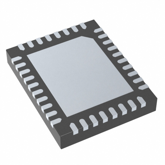


 工商网监
湘ICP备2023018690号
工商网监
湘ICP备2023018690号
