LTM4603/LTM4603-1
20V, 6A DC/DC µModule
Regulator with PLL, Output
Tracking and Margining
Description
Features
n
n
n
n
n
n
n
n
n
n
n
n
Complete Switch Mode Power Supply
Wide Input Voltage Range: 4.5V to 20V
6A DC Typical, 8A Peak Output Current
0.6V to 5V Output Voltage
Output Voltage Tracking and Margining
Remote Sensing for Precision Regulation (LTM4603
Only)
Typical Operating Frequency: 1MHz
PLL Frequency Synchronization
1.5% Regulation
Current Foldback Protection (Disabled at Start-Up)
Pin Compatible with the LTM4601
Pb-Free (e4) RoHS Compliant Package with Gold
Finish Pads
Ultrafast Transient Response
Current Mode Control
Up to 93% Efficiency at 5VIN, 3.3VOUT
Programmable Soft-Start
Output Overvoltage Protection
Small Footprint, Low Profile (15mm × 15mm ×
2.82mm) Surface Mount LGA Package
Applications
Telecom and Networking Equipment
Servers
n Industrial Equipment
n Point of Load Regulation
n
n
The LTM®4603 is a complete 6A step-down switch mode
DC/DC µModule® regulator with onboard switching controller, MOSFETs, inductor and all support components.
The device is housed in a small surface mount 15mm ×
15mm × 2.82mm LGA package. Operating over an input
voltage range of 4.5V to 20V, the LTM4603 supports an
output voltage range of 0.6V to 5V as well as output voltage tracking and margining. The high efficiency design
delivers 6A continuous current (8A peak). Only bulk input
and output capacitors are needed to complete the design.
The low profile (2.82mm) and light weight (1.7g) package
easily mounts on the unused space on the back side of
PC boards for high density point of load regulation. The
µModule regulator can be synchronized with an external
clock for reducing undesirable frequency harmonics and
allows PolyPhase® operation for high load currents.
A high switching frequency and adaptive on-time current
mode architecture deliver a very fast transient response
to line and load changes without sacrificing stability. An
onboard remote sense amplifier can be used to accurately
regulate an output voltage independent of load current.
The onboard remote sense amplifier is not available in the
LTM4603-1. The LTM4603/LTM4603-1 are pin compatible
with the 12A LTM4601/LTM4601-1.
L, LT, LTC, LTM, Linear Technology, the Linear logo, µModule and PolyPhase are registered
trademarks and LTpowerCAD is a trademark of Linear Technology Corporation. All other
trademarks are the property of their respective owners.
Typical Application
Efficiency vs Load Current with 12VIN
1.5V/6A Power Supply with 4.5V to 20V Input
100
95
CLOCK SYNC
TRACK/SS CONTROL
VIN
4.5V TO 20V
VIN
PGOOD
ON/OFF
CIN
392k
5% MARGIN
RUN
COMP
INTVCC
DRVCC
MPGM
SGND
PLLIN TRACK/SS
VOUT
LTM4603
PGND
VFB
MARG0
MARG1
VOUT_LCL
DIFFVOUT
VOSNS+
VOSNS–
100pF
MARGIN
CONTROL
90
VOUT
1.5V
6A
COUT
85
EFFICIENCY (%)
n
n
n
n
n
n
80
75
70
65
12VIN, 1.2VOUT
12VIN, 1.5VOUT
12VIN, 1.8VOUT
12VIN, 2.5VOUT
12VIN, 3.3VOUT
12VIN, 5VOUT
60
55
40.2k
50
45
40
fSET
4603 TA01a
0
1
4
3
2
5
LOAD CURRENT (A)
6
7
4603 TA01b
4603fb
1
�LTM4603/LTM4603-1
Absolute Maximum Ratings
(Note 1)
Pin Configuration
INTVCC, DRVCC, VOUT_LCL, VOUT (VOUT ≤ 3.3V
with Remote Sense Amp)............................. –0.3V to 6V
PLLIN, TRACK/SS, MPGM, MARG0, MARG1,
PGOOD, fSET...............................–0.3V to INTVCC + 0.3V
RUN.............................................................. –0.3V to 5V
VFB, COMP................................................. –0.3V to 2.7V.
VIN.............................................................. –0.3V to 20V
VOSNS+, VOSNS –...........................–0.3V to INTVCC + 0.3V
Operating Temperature Range (Note 2)....–40°C to 85°C
Junction Temperature............................................ 125°C
Storage Temperature Range................... –55°C to 125°C
INTVCC
PLLIN
TRACK/SS
RUN
COMP
MPGM
TOP VIEW
VIN
fSET
MARG0
MARG1
DRVCC
VFB
PGOOD
SGND
VOSNS+/NC2*
DIFFVOUT/NC3*
VOUT_LCL
VOSNS–/NC1*
PGND
VOUT
LGA PACKAGE
118-LEAD (15mm × 15mm × 2.82mm)
TJMAX = 125°C, θJA = 15°C/W, θJC = 6°C/W
θJA DERIVED FROM 95mm × 76mm PCB WITH 4 LAYERS, WEIGHT = 1.7g
*LTM4603-1 ONLY
Order Information
LEAD FREE FINISH
TRAY
PART MARKING*
PACKAGE DESCRIPTION
TEMPERATURE RANGE †
LTM4603EV#PBF
LTM4603EV#PBF
LTM4603V
118-Lead (15mm × 15mm × 2.82mm) LGA
–40°C to 85°C
LTM4603IV#PBF
LTM4603IV#PBF
LTM4603V
118-Lead (15mm × 15mm × 2.82mm) LGA
–40°C to 85°C
LTM4603EV-1#PBF
LTM4603EV-1#PBF
LTM4603V-1
118-Lead (15mm × 15mm × 2.82mm) LGA
–40°C to 85°C
LTM4603IV-1#PBF
LTM4603IV-1#PBF
LTM4603V-1
118-Lead (15mm × 15mm × 2.82mm) LGA
–40°C to 85°C
Consult LTC Marketing for parts specified with wider operating temperature ranges. *The temperature grade is identified by a label on the shipping container.
† See Note 2.
For more information on lead free part marking, go to: http://www.linear.com/leadfree/
This product is only offered in trays. For more information go to: http://www.linear.com/packaging/
Electrical Characteristics
The l denotes the specifications which apply over the –40°C to 85°C
operating temperature range (Note 2), otherwise specifications are at TA = 25°C, VIN = 12V, per typical application (front page)
configuration.
SYMBOL
PARAMETER
VIN(DC)
Input DC Voltage
VOUT(DC)
Output Voltage
CONDITIONS
CIN = 10µF ×2, COUT = 2× 100µF X5R Ceramic
VIN = 5V, VOUT = 1.5V, IOUT = 0A
VIN = 12V, VOUT = 1.5V, IOUT = 0A
MIN
l
4.5
l
l
1.478
1.478
TYP
MAX
UNITS
20
V
1.5
1.5
1.522
1.522
V
V
4
V
Input Specifications
VIN(UVLO)
Undervoltage Lockout Threshold
IOUT = 0A
3.2
IINRUSH(VIN)
Input Inrush Current at Start-Up
IOUT = 0A. VOUT = 1.5V
VIN = 5V
VIN = 12V
0.6
0.7
2
A
A
4603fb
�LTM4603/LTM4603-1
ELECTRICAL CHARACTERISTICS
The l denotes the specifications which apply over the –40°C to 85°C
operating temperature range (Note 2), otherwise specifications are at TA = 25°C, VIN = 12V, per typical application (front page)
configuration.
SYMBOL
PARAMETER
CONDITIONS
IQ(VIN,NOLOAD)
Input Supply Bias Current
VIN = 12V, No Switching
VIN = 12V, VOUT = 1.5V, Switching Continuous
VIN = 5V, No Switching
VIN = 5V, VOUT = 1.5V, Switching Continuous
Shutdown, RUN = 0, VIN = 12V
IS(VIN)
Input Supply Current
VIN = 12V, VOUT = 1.5V, IOUT = 6A
VIN = 12V, VOUT = 3.3V, IOUT = 6A
VIN = 5V, VOUT = 1.5V, IOUT = 6A
INTVCC
VIN = 12V, RUN > 2V
No Load
MIN
4.7
TYP
MAX
UNITS
3.8
25
mA
mA
2.5
43
mA
mA
22
µA
0.92
1.83
2.12
A
A
A
5
5.3
V
6
A
Output Specifications
IOUTDC
Output Continuous Current Range
VIN = 12V, VOUT = 1.5V (Note 5)
0
∆VOUT(LINE)
Line Regulation Accuracy
VOUT = 1.5V, IOUT = 0A, VIN = 4.5V to 20V
l
0.3
%
Load Regulation Accuracy
VOUT = 1.5V, IOUT = 0A to 6A (Note 5)
VIN = 12V, with Remote Sense Amp
VIN = 12V, LTM4603-1
l
l
0.25
0.5
%
%
VOUT
∆VOUT(LOAD)
VOUT
VOUT(AC)
Output Ripple Voltage
IOUT = 0A, COUT = 2× 100µF X5R Ceramic
VIN = 12V, VOUT = 1.5V
VIN = 5V, VOUT = 1.5V
fS
Output Ripple Voltage Frequency
IOUT = 3A, VIN = 12V, VOUT = 1.5V
ΔVOUT(START)
Turn-On Overshoot
10
10
mVP-P
mVP-P
1000
kHz
COUT = 200µF, VOUT = 1.5V, IOUT = 0A,
TRACK/SS = 10nF
VIN = 12V
VIN = 5V
20
20
mV
mV
COUT = 200µF, VOUT = 1.5V, TRACK/SS = Open,
IOUT = 1A Resistive Load
VIN = 12V
VIN = 5V
0.5
0.5
ms
ms
Load: 0% to 50% to 0% of Full Load,
COUT = 2 × 22µF Ceramic, 470µF 4V
Sanyo POSCAP
VIN = 12V
VIN = 5V
35
35
mV
mV
tSETTLE
Settling Time for Dynamic Load Step Load: 0% to 50% to 10% of Full Load
VIN = 12V
25
µs
IOUTPK
Output Current Limit
8
8
A
A
tSTART
ΔVOUTLS
Turn-On Time
Peak Deviation for Dynamic Load
COUT = 2× 100µF X5R Ceramic
VIN = 12V, VOUT = 1.5V
VIN = 5V, VOUT = 1.5V
Remote Sense Amp (LTM4603 Only, Not Supported in the LTM4603-1) (Note 3)
VOSNS+, VOSNS–
CM Range
Common Mode Input Voltage Range VIN = 12V, RUN > 2V
0
INTVCC – 1
0
INTVCC – 1
VIN = 12V, DIFFVOUT Load = 100k
V
DIFFVOUT Range
Output Voltage Range
VOS
Input Offset Voltage Magnitude
AV
Differential Gain
1
V/V
GBP
Gain Bandwidth Product
3
MHz
SR
Slew Rate
2
V/µs
1.25
V
mV
4603fb
3
�LTM4603/LTM4603-1
ELECTRICAL CHARACTERISTICS
The l denotes the specifications which apply over the –40°C to 85°C
operating temperature range (Note 2), otherwise specifications are at TA = 25°C, VIN = 12V, per typical application (front page)
configuration.
SYMBOL
PARAMETER
RIN
Input Resistance
CMRR
Common Mode Rejection Ratio
CONDITIONS
MIN
+ to GND
VOSNS
TYP
MAX
UNITS
20
kW
100
dB
Control Stage
VFB
Error Amplifier Input Voltage
Accuracy
IOUT = 0A, VOUT = 1.5V
l
0.594
0.6
0.606
V
1
1.5
1.9
V
–1
–1.5
–2
µA
VRUN
RUN Pin On/Off Threshold
ITRACK/SS
Soft-Start Charging Current
VTRACK/SS = 0V
tON(MIN)
Minimum On Time
(Note 4)
50
100
ns
tOFF(MIN)
Minimum Off Time
(Note 4)
250
400
ns
RPLLIN
PLLIN Input Resistance
IDRVCC
Current into DRVCC Pin
RFBHI
Resistor Between VOUT_LCL and VFB
VMPGM
Margin Reference Voltage
1.18
V
VMARG0, VMARG1
MARG0, MARG1 Voltage Thresholds
1.4
V
50
VOUT = 1.5V, IOUT = 1A, DRVCC = 5V
60.098
kΩ
20
27
mA
60.4
60.702
kΩ
PGOOD Output
ΔVFBH
PGOOD Upper Threshold
VFB Rising
7
10
13
%
ΔVFBL
PGOOD Lower Threshold
VFB Falling
–7
–10
–13
%
ΔVFB(HYS)
PGOOD Hysteresis
VFB Returning (Note 4)
1.5
3
%
VPGL
PGOOD Low Voltage
IPGOOD = 5mA
0.15
0.4
V
Note 1: Stresses beyond those listed under Absolute Maximum Ratings
may cause permanent damage to the device. Exposure to any Absolute
Maximum Rating condition for extended periods may affect device
reliability and lifetime.
Note 2: The LTM4603/LTM4603-1 is tested under pulsed load conditions
such that TJ ≈ TA. The LTM4603E/LTM4603E-1 are guaranteed to meet
performance specifications from 0°C to 85°C. Specifications over the
–40°C to 85°C operating temperature range are assured by design,
characterization and correlation with statistical process controls. The
LTM4603I/LTM4603I-1 are guaranteed over the –40°C to 85°C operating
temperature range.
4
Note 3: Remote sense amplifier recommended for ≤3.3V output.
Note 4: 100% tested at wafer sort only.
Note 5: See output current derating curves for different VIN, VOUT and TA.
4603fb
�LTM4603/LTM4603-1
Typical Performance Characteristics (See Figure 18 for all curves)
Efficiency vs Load Current
with 5VIN
100
100
95
95
95
90
90
85
85
80
EFFICIENCY (%)
85
80
75
70
5VIN, 0.6VOUT
5VIN, 1.2VOUT
5VIN, 1.5VOUT
5VIN, 1.8VOUT
5VIN, 2.5VOUT
5VIN, 3.3VOUT
65
60
55
50
0
1
4
3
2
5
LOAD CURRENT (A)
80
75
70
65
12VIN, 1.2VOUT
12VIN, 1.5VOUT
12VIN, 1.8VOUT
12VIN, 2.5VOUT
12VIN, 3.3VOUT
12VIN, 5VOUT
60
55
50
45
6
40
7
EFFICIENCY (%)
90
EFFICIENCY (%)
Efficiency vs Load Current
with 20VIN
Efficiency vs Load Current
with 12VIN
0
1
4
3
2
5
LOAD CURRENT (A)
6
75
70
65
60
20VIN, 1.5VOUT
20VIN, 1.8VOUT
20VIN, 2.5VOUT
20VIN, 3.3VOUT
20VIN, 5VOUT
55
50
45
7
40
0
4
3
2
5
LOAD CURRENT (A)
4603 G02
4603 G01
1.2V Transient Response
1.5V Transient Response
LOAD STEP
1A/DIV
VOUT
50mV/DIV
VOUT
50mV/DIV
VOUT
50mV/DIV
25µs/DIV
1.5V AT 3A/µs LOAD STEP
COUT: 1× 22µF, 6.3V CERAMIC
1× 330µF, 4V SANYO POSCAP
2.5V Transient Response
4603 G05
25µs/DIV
1.8V AT 3A/µs LOAD STEP
COUT: 1× 22µF, 6.3V CERAMIC
1× 330µF, 4V SANYO POSCAP
4603 G06
3.3V Transient Response
LOAD STEP
1A/DIV
LOAD STEP
1A/DIV
VOUT
50mV/DIV
VOUT
50mV/DIV
25µs/DIV
2.5V AT 3A/µs LOAD STEP
COUT: 1× 22µF, 6.3V CERAMIC
1× 330µF, 4V SANYO POSCAP
7
1.8V Transient Response
LOAD STEP
1A/DIV
4603 G04
6
4603 G03
LOAD STEP
1A/DIV
25µs/DIV
1.2V AT 3A/µs LOAD STEP
COUT: 1× 22µF, 6.3V CERAMIC
1× 330µF, 4V SANYO POSCAP
1
4603 G07
25µs/DIV
3.3V AT 3A/µs LOAD STEP
COUT: 1× 22µF, 6.3V CERAMIC
1× 330µF, 4V SANYO POSCAP
4603 G08
4603fb
5
�LTM4603/LTM4603-1
TYPICAL PERFORMANCE CHARACTERISTICS (See Figure 18 for all curves)
Start-Up, IOUT = 6A
(Resistive Load)
Start-Up, IOUT = 0A
Short-Circuit Protection,
IOUT = 0A
VOUT
0.5V/DIV
VOUT
0.5V/DIV
VOUT
0.5V/DIV
IIN
0.5A/DIV
IIN
0.5A/DIV
1ms/DIV
VIN = 12V
VOUT = 1.5V
COUT = 1× 22µF, 6.3V CERAMIC
1× 330µF, 4V SANYO POSCAP
SOFT-START = 3.9nF
IIN
2A/DIV
1ms/DIV
VIN = 12V
VOUT = 1.5V
COUT = 1× 22µF, 6.3V CERAMIC
1× 330µF, 4V SANYO POSCAP
SOFT-START = 3.9nF
4603 G09
Short-Circuit Protection,
IOUT = 6A
4603 G10
VIN to VOUT Step-Down Ratio
5.5
3.3V OUTPUT WITH
82.5k FROM VOUT
TO fSET
5.0
4.5
OUTPUT VOLTAGE (V)
VOUT
0.5V/DIV
IIN
2A/DIV
100µs/DIV
VIN = 12V
VOUT = 1.5V
COUT = 1× 22µF, 6.3V CERAMIC
1× 330µF, 4V SANYO POSCAP
SOFT-START = 3.9nF
4603 G11
100µs/DIV
VIN = 12V
VOUT = 1.5V
COUT = 1× 22µF, 6.3V CERAMIC
1× 330µF, 4V SANYO POSCAP
SOFT-START = 3.9nF
4603 G12
5V OUTPUT WITH
150k RESISTOR
ADDED FROM fSET
TO GND
4.0
3.5
3.0
2.0
5V OUTPUT WITH
NO RESISTOR ADDED
FROM fSET TO GND
1.5
2.5V OUTPUT
1.0
1.8V OUTPUT
0.5
1.5V OUTPUT
2.5
0
1.2V OUTPUT
0
2
4
6 8 10 12 14 16 18 20
INPUT VOLTAGE (V)
4603 G13
6
4603fb
�LTM4603/LTM4603-1
Pin Functions (See Package Description for Pin Assignment)
VIN (Bank 1): Power Input Pins. Apply input voltage between these pins and PGND pins. Recommend placing
input decoupling capacitance directly between VIN pins
and PGND pins.
VOUT (Bank 3): Power Output Pins. Apply output load
between these pins and PGND pins. Recommend placing
output decoupling capacitance directly between these pins
and PGND pins. See Figure 15.
PGND (Bank 2): Power ground pins for both input and
output returns.
VOSNS– (Pin M12): (–) Input to the Remote Sense Amplifier. This pin connects to the ground remote sense point.
The remote sense amplifier is used for VOUT ≤ 3.3V. Tie
to INTVCC if not used.
NC1 (Pin M12): No internal connection on the LTM4603-1.
VOSNS+ (Pin J12): (+) Input to the Remote Sense Amplifier. This pin connects to the output remote sense point.
The remote sense amplifier is used for VOUT ≤ 3.3V. Tie
to ground if not used.
NC2 (Pin J12): No internal connection on the LTM4603-1.
DIFFVOUT (Pin K12): Output of the Remote Sense Amplifier. This pin connects to the VOUT_LCL pin. Leave floating
if remote sense amplifier is not used.
NC3 (Pin K12): No internal connection on the LTM4603-1.
DRVCC (Pin E12): This pin normally connects to INTVCC
for powering the internal MOSFET drivers. This pin can
be biased up to 6V from an external supply with about
50mA capability, or an external circuit shown in Figure
16. This improves efficiency at the higher input voltages
by reducing power dissipation in the module.
INTVCC (Pin A7): This pin is for additional decoupling of
the 5V internal regulator.
PLLIN (Pin A8): External Clock Synchronization Input
to the Phase Detector. This pin is internally terminated
to SGND with a 50k resistor. Apply a clock with a high
level above 2V and below INTVCC. See the Applications
Information section.
TRACK/SS (Pin A9): Output Voltage Tracking and SoftStart Pin. When the module is configured as a master
output, then a soft-start capacitor is placed on this pin
to ground to control the master ramp rate. A soft-start
capacitor can be used for soft-start turn on as a stand
alone regulator. Slave operation is performed by putting
a resistor divider from the master output to ground, and
connecting the center point of the divider to this pin. See
the Applications Information section.
MPGM (Pin A12): Programmable Margining Input. A resistor from this pin to ground sets a current that is equal
to 1.18V/R. This current multiplied by 10kΩ will equal a
value in millivolts that is a percentage of the 0.6V reference voltage. See Applications Information. To parallel
LTM4603s, each requires an individual MPGM resistor.
Do not tie MPGM pins together.
INTVCC
PLLIN
TRACK/SS
RUN
COMP
MPGM
TOP VIEW
A
VIN
B
BANK 1
C
D
E
PGND
F
BANK 2
G
H
J
VOUT K
BANK 3 L
M
fSET
MARG0
MARG1
DRVCC
VFB
PGOOD
SGND
VOSNS+ (NC2, LTM4603-1)
DIFFVOUT (NC3, LTM4603-1)
VOUT_LCL
VOSNS– (NC1, LTM4603-1)
1 2 3 4 5 6 7 8 9 10 11 12
4603fb
7
�LTM4603/LTM4603-1
PIN FUNCTIONS (See Package Description for Pin Assignment)
fSET (Pin B12): Frequency Set Internally to 1MHz. An
external resistor can be placed from this pin to ground
to increase frequency. See the Applications Information
section for frequency adjustment.
VFB (Pin F12): The Negative Input of the Error Amplifier. Internally, this pin is connected to VOUT_LCL with a
60.4k precision resistor. Different output voltages can be
programmed with an additional resistor between VFB and
SGND pins. See the Applications Information section.
MARG0 (Pin C12): This pin is the LSB logic input for the
margining function. Together with the MARG1 pin it will
determine if margin high, margin low or no margin state
is applied. The pin has an internal pull-down resistor of
50k. See the Applications Information section.
MARG1 (Pin D12): This pin is the MSB logic input for the
margining function. Together with the MARG0 pin it will
determine if margin high, margin low or no margin state
is applied. The pin has an internal pull-down resistor of
50k. See the Applications Information section.
SGND (Pin H12): Signal Ground. This pin connects to
PGND at output capacitor point.
8
COMP (Pin A11): Current Control Threshold and Error
Amplifier Compensation Point. The current comparator
threshold increases with this control voltage. The voltage
ranges from 0V to 2.4V with 0.7V corresponding to zero
sense voltage (zero current).
PGOOD (Pin G12): Output Voltage Power Good Indicator.
Open-drain logic output that is pulled to ground when the
output voltage is not within ±10% of the regulation point,
after a 25µs power bad mask timer expires.
RUN (Pin A10): Run Control Pin. A voltage above 1.9V
will turn on the module, and when below 1V, will turn
off the module. A programmable UVLO function can be
accomplished by connecting to a resistor divider from
VIN to ground. See Figure 1. This pin has a 5.1V Zener to
ground. Maximum pin voltage is 5V. Limit current into the
RUN pin to less than 1mA.
VOUT_LCL (Pin L12): VOUT connects directly to this pin to
bypass the remote sense amplifier, or DIFFVOUT connects
to this pin when the remote sense amplifier is used.
VOUT_LCL can be connected to VOUT on the LTM4603-1.
VOUT is internally connected to VOUT_LCL through 50Ω in
the LTM4603-1.
4603fb
�LTM4603/LTM4603-1
Simplified Block Diagram
VOUT_LCL
VIN
R1
UVLO
FUNCTION
>1.9V = ON
4.8V use 4.8V
LTM4603 minimum on-time = 100ns
tON = [(VOUT • 10pF)/IfSET]
LTM4603 minimum off-time = 400ns
tOFF = t – tON, where t = 1/Frequency
LTM4603 minimum off-time = 400ns
tOFF = t – tON, where t = 1/Frequency
Duty Cycle = tON/t or VOUT/VIN
Duty Cycle (DC) = tON /t or VOUT /VIN
Equations for setting frequency:
Equations for setting frequency:
IfSET = (VIN/(3 • RfSET)), for 20V operation, IfSET = 201µA, tON
= [(4.8 • 10pF)/IfSET], tON = 239ns, where the internal RfSET
is 33.2k. Frequency = (VOUT/(VIN • tON)) = (5V/(20 • 239ns))
~ 1MHz. The inductor ripple current begins to get high at
the higher input voltages due to a larger voltage across the
inductor. This is noted in the Inductor Ripple Current vs
Duty Cycle graph at ~5A at 25% duty cycle. The inductor
ripple current can be lowered at the higher input voltages by
adding an external resistor from fSET to ground to increase
the switching frequency. A 3A ripple current is chosen, and
the total peak current is equal to 1/2 of the 3A ripple current
plus the output current. The 5V output current is limited
to 5A, so total peak current is less than 6.5A. This is below
the 7A peak specified value. A 150k resistor is placed from
fSET to ground, and the parallel combination of 150k and
33.2k equates to 27.2k. The IfSET calculation with 27.2k
and 20V input voltage equals 245µA. This equates to a tON
of 196ns. This will increase the switching frequency from
1MHz to ~1.28MHz for the 20V to 5V conversion. The
minimum on time is above 100ns at 20V input. Since
the switching frequency is approximately constant over
input and output conditions, then the lower input voltage
range is limited to 10V for the 1.28MHz operation due to
the 400ns minimum off time. Equation: tON = (VOUT/VIN)
• (1/Frequency) equates to a 382ns on time, and a 400ns
off time. The VIN to VOUT Step-Down Ratio curve reflects
an operating range of 10V to 20V for 1.28MHz operation
with a 150k resistor to ground, and an 8V to 16V operation
for fSET floating. These modifications are made to provide
wider input voltage ranges for the 5V output designs while
limiting the inductor ripple current, and maintaining the
400ns minimum off time.
IfSET = [VIN/(3 • RfSET)], for 20V operation, IfSET = 201µA,
tON = [(3.3 • 10pF)/IfSET], tON = 164ns, where the internal
RfSET is 33.2k. Frequency = [VOUT/(VIN • tON)] = [3.3V/
(20•164ns)] ~ 1MHz. The minimum on-time and minimum
off-time are within specification at 164ns and 836ns.
However, the 4.5V input to 3.3V output circuit will not meet
the minimum off-time specification of 400ns (tON = 733ns,
Frequency = 1MHz, tOFF = 267ns).
20
Solution
Lower the switching frequency at lower input voltages to
allow for higher duty cycles, and meet the 400ns minimum
off-time at 4.5V input voltage. The off-time should be about
500ns with 100ns guard band included. The duty cycle
for (3.3V/4.5V) = ~73%. Frequency = (1 – DC)/tOFF, or
(1 – 0.73)/500ns = 540kHz. The switching frequency needs
to be lowered to 540kHz at 4.5V input. tON = DC/frequency,
or 1.35µs. The fSET pin voltage is 1/3 of VIN, and the IfSET
current equates to 45µA with the internal 33.2k. The IfSET
current needs to be 24µA for 540kHz operation. A resistor
can be placed from VOUT to fSET to lower the effective IfSET
current out of the fSET pin to 24µA. The fSET pin is 4.5V/3
=1.5V and VOUT = 3.3V, therefore 82.5k will source 21µA
into the fSET node and lower the IfSET current to 24µA.
This enables the 540kHz operation and the 4.5V to 20V
input operation for down converting to 3.3V output. The
frequency will scale from 540kHz to 1.2MHz over this
input range. This provides for an effective output current
of 5A over the input range.
4603fb
�LTM4603/LTM4603-1
APPLICATIONS INFORMATION
VOUT
VIN
10V TO 20V
C2
10µF
25V
R2
100k
TRACK/SS CONTROL
R4
100k
VIN
PGOOD
MPGM
RUN
COMP
INTVCC
DRVCC
5% MARGIN
R1
392k
1%
C1
10µF
25V
PLLIN TRACK/SS
VOUT
LTM4603
SGND
PGND
VFB
MARG0
MARG1
REVIEW TEMPERATURE
DERATING CURVE
C3
100µF
REFER TO
6.3V
SANYO POSCAP TABLE 2
+
C6 100pF
VOUT_LCL
DIFFVOUT
VOSNS–
VOSNS+
VOUT
5V
5A
INTVCC
fSET
RfSET
150k
RSET
8.25k
MARGIN CONTROL
IMPROVE
EFFICIENCY
FOR ≥12V INPUT
SOT-323
DUAL
CMSSH-3C3
4603 F16
Figure 16. 5V at 5A Design Without Differential Amplifier
VOUT
VIN
4.5V TO 20V
TRACK/SS CONTROL
R2
100k
R4
100k
PGOOD
C2
10µF
25V
VIN
PGOOD
MPGM
RUN
COMP
INTVCC
DRVCC
PLLIN TRACK/SS
VOUT
LTM4603
R1
392k
C1
10µF
25V
5% MARGIN
SGND
PGND
REVIEW TEMPERATURE
DERATING CURVE
VFB
MARG0
MARG1
VOUT_LCL
DIFFVOUT
VOSNS+
VOSNS–
fSET
MARGIN CONTROL
C6 100pF
+
RfSET
82.5k
VOUT
3.3V
5A
C3
100µF
6.3V
SANYO POSCAP
RSET
13.3k
4603 F17
Figure 17. 3.3V at 5A Design
4603fb
21
�LTM4603/LTM4603-1
APPLICATIONS INFORMATION
CLOCK SYNC
VOUT
VIN
4.5V TO 20V
R2
100k
C5
0.01µF
R4
100k
PGOOD
CIN
BULK
OPT.
TABLE 2
+
CIN
10µF
25V
×2 CER
PLLIN TRACK/SS
VOUT
VIN
PGOOD
MPGM
RUN
ON/OFF
COMP
INTVCC
DRVCC
R1
392k
LTM4603
SGND
PGND
VFB
MARG0
MARG1
REVIEW TEMPERATURE
DERATING CURVE
C3 100pF
COUT1
22µF
6.3V
MARGIN
CONTROL
+
COUT2
470µF
6.3V
VOUT
1.5V
6A
VOUT_LCL
DIFFVOUT
VOSNS+
VOSNS–
fSET
RSET
40.2k
REFER TO
TABLE 2
4603 F18
5% MARGIN
Figure 18. Typical 4.5V to 20VIN, 1.5V at 6A Design
CLOCK SYNC 0° PHASE
C10
10µF
25V
C1
10µF
25V
R1
100k
R2
100k
R9
60.4k
VIN
PGOOD
MPGM
RUN
COMP
INTVCC
DRVCC
C12
0.1µF
PLLIN TRACK/SS
VOUT
LTM4603
LTC6908-1
1
R11
118k
2
3
V+
OUT1
GND
OUT2
SET
MOD
2.5V
1.2V
4.5V TO 16V
4
R5
392k
5
SGND
PGND
VFB
MARG0
MARG1
R10
60.4k
1.2V AT 6A
C6 100pF
C4
22µF
6.3V
MARGIN
CONTROL
C5
470µF
6.3V
VOUT_LCL
DIFFVOUT
VOSNS+
VOSNS–
fSET
+
R7
60.4k
6
2-PHASE
OSCILLATOR
CLOCK SYNC 180° PHASE
+
C11*
100µF
25V
C3
0.01µF
2.5V
4.5V TO 16V
C2
10µF
25V
R3
100k
R4
100k
VIN
PGOOD
MPGM
RUN
COMP
INTVCC
DRVCC
R6
392k
PLLIN TRACK/SS
VOUT
LTM4603
SGND
PGND
VFB
MARG0
MARG1
2.5V AT 6A
C6 100pF
C7
22µF
6.3V
MARGIN
CONTROL
C8
470µF
6.3V
VOUT_LCL
DIFFVOUT
VOSNS+
VOSNS–
fSET
*C11 OPTIONAL TO REDUCE LC RINGING.
NOT NEEDED FOR LOW INDUCTANCE PLANE CONNECTIONS
+
R8
19.1k
4603 F19
Figure 19. 2-Phase, 2.5V and 1.2V at 6A with Coincident Tracking
22
4603fb
�+
C11
100µF
35V
OPT
INTERMEDIATE
BUS
C2
10µF
25V
×2
R1
392k
ON/OFF
R3
100k
8V TO 16V
5% MARGIN
PGOOD
R2
100k
3.3V
5% MARGIN
C8
10µF
25V
×2
VIN
PGOOD
SGND
MPGM
RUN
COMP
INTVCC
DRVCC
VIN
PGOOD
SGND
MPGM
RUN
ON/OFF
COMP
INTVCC
DRVCC
R27
392k
R7
100k
PGOOD
R6
100k
8V TO 16V
3.3V OR
APPROPRIATE
–48V
INPUT
fSET
VOUT_LCL
DIFFVOUT
VOSNS+
VOSNS–
PGND
LTM4603
fSET
VOUT_LCL
DIFFVOUT
VOSNS+
VOSNS–
VFB
MARG0
MARG1
PLLIN TRACK/SS
VOUT
CLOCK SYNC 3
PGND
LTM4603
VFB
MARG0
MARG1
PLLIN TRACK/SS
VOUT
MARGIN
CONTROL
C8 100pF
R19
30.1k
MARGIN
CONTROL
R8
13.3k
R12
30.1k
R21
60.4k
C7
0.15µF
C12 100pF
TRACK/SS
CONTROL
CLOCK SYNC 1
3.3V
+
REFER TO
TABLE 2
C3
22µF
6.3V
R17
59k
LTC6902
+
C4
470µF
6.3V
C10
470µF
6.3V
V+
SET
DIV
MOD
PH
GND
OUT1 OUT4
OUT2 OUT3
1.8V AT 6A
REFER TO
TABLE 2
C9
22µF
6.3V
3.3V AT 5A
4-PHASE
OSCILLATOR
8V TO 16V
C26
0.1µF
C14
10µF
25V
×2
R14
392k
ON/OFF
R16
100k
5% MARGIN
PGOOD
R15
100k
8V TO 16V
5% MARGIN
3.3V
C14
10µF
25V
×2
VIN
PGOOD
PGND
LTM4603
SGND
MPGM
RUN
COMP
INTVCC
DRVCC
VIN
PGOOD
PGND
LTM4603
fSET
VOUT_LCL
DIFFVOUT
VOSNS+
VOSNS–
VFB
MARG0
MARG1
PLLIN TRACK/SS
VOUT
fSET
VOUT_LCL
DIFFVOUT
VOSNS+
VOSNS–
VFB
MARG0
MARG1
PLLIN TRACK/SS
VOUT
CLOCK SYNC 4
SGND
MPGM
RUN
ON/OFF
COMP
INTVCC
DRVCC
R9
392k
R11
100k
PGOOD
R10
100k
3.3V 8V TO 16V
CLOCK SYNC 2
4-Phase, Four Outputs (3.3V, 2.5V, 1.8V and 1.5V) with Coincident Tracking
MARGIN
CONTROL
C24 100pF
R26
40.2k
MARGIN
CONTROL
C18 100pF
R24
19.1k
R13
40.2k
R25
60.4k
R18
19.1k
R23
60.4k
3.3V
3.3V
+
REFER TO
TABLE 2
C16
22µF
6.3V
+
1.5V AT 6A
REFER TO
TABLE 2
C16
22µF
6.3V
2.5V AT 6A
C15
470µF
6.3V
C15
470µF
6.3V
LTM4603/LTM4603-1
Typical Application
23
4603fb
�C(0.30)
PAD 1
1.27
BSC
13.97
BSC
0.12 – 0.28
6.9850
5.7150
4.4450
3.1750
1.9050
0.6350
0.0000
0.6350
1.9050
3.1750
4.4450
5.7150
6.9850
6.9850
1
5.7150
2
4.4450
3.1750
1.9050
0.6350
0.0000
0.6350
1.9050
3.1750
4.4450
3
4
6
7
8
BOTTOM VIEW
5
13.97
BSC
9
10
SUGGESTED SOLDER PAD LAYOUT
TOP VIEW
6.9850
5.7150
11
12
DETAIL A
PADS
SEE NOTES
3
A
eee M X Y
0.27 – 0.37
SUBSTRATE
DETAIL A
0.60 – 0.66
DETAIL B
MOLD
CAP
DETAIL B
2.72 – 2.92
4
PAD 1
CORNER
aaa Z
(Reference LTC DWG # 05-08-1801 Rev Ø)
0.60 – 0.66
B
C
D
E
F
G
H
J
K
L
M
2.45 – 2.55
bbb Z
24
Z
LGA Package
118-Lead (15mm × 15mm)
X
DETAILS OF PAD #1 IDENTIFIER ARE OPTIONAL,
BUT MUST BE LOCATED WITHIN THE ZONE INDICATED.
THE PAD #1 IDENTIFIER MAY BE EITHER A MOLD OR
MARKED FEATURE
4
SYMBOL TOLERANCE
aaa
0.10
bbb
0.10
eee
0.03
LGA 118 0306 REV Ø
6. THE TOTAL NUMBER OF PADS: 118
5. PRIMARY DATUM -Z- IS SEATING PLANE
LAND DESIGNATION PER JESD MO-222, SPP-010
3
2. ALL DIMENSIONS ARE IN MILLIMETERS
NOTES:
1. DIMENSIONING AND TOLERANCING PER ASME Y14.5M-1994
TOP VIEW
15
BSC
15
BSC
Y
aaa Z
LTM4603/LTM4603-1
Package Description
Please refer to http://www.linear.com/designtools/packaging/ for the most recent package drawings.
4603fb
�LTM4603/LTM4603-1
Revision History
(Revision history begins at Rev B)
REV
DATE
DESCRIPTION
B
8/11
Updated Note 2 test parameters.
PAGE NUMBER
4
Updated the usage of Remote Sense Amplifier pins.
7
Updated the fSET pin description.
8
Updated the Simplified Block Diagram.
9
Added additional information for the tracking applications.
14
Updated the Frequency Adjustment section and equations.
19, 20
Updated the example circuits.
22, 23
Added a package photo.
26
Updated the Related Parts information.
26
4603fb
Information furnished by Linear Technology Corporation is believed to be accurate and reliable.
However, no responsibility is assumed for its use. Linear Technology Corporation makes no representation that the interconnection of its circuits as described herein will not infringe on existing patent rights.
25
�LTM4603/LTM4603-1
Typical Application
3.3V at 5A, LTM4603-1 (No Remote Sense Amplifier)
VIN
4.5V TO 20V
R2
100k
R4
100k
PGOOD
R1
392k
C2
10µF
35V
TRACK/SS
CONTROL
MPGM
RUN
COMP
INTVCC
DRVCC
C1
10µF
35V
REVIEW TEMPERATURE
DERATING CURVE
VOUT
3.3V
C6
5A
+
100pF
C3
100µF
6.3V
PLLIN TRACK/SS
VOUT
VIN
PGOOD
LTM4603-1
SGND
5% MARGIN
PGND
VFB
MARG0
MARG1
VOUT_LCL
NC3
NC2
NC1
RfSET
82.5k
RSET
13.3k
fSET
4603 TA05
MARGIN CONTROL
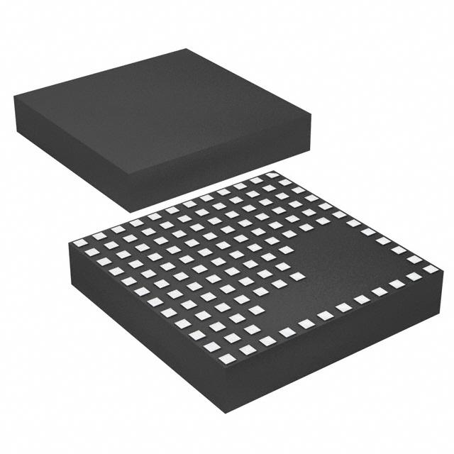
Package Photograph
15mm
2.82mm
15mm
Related Parts
PART NUMBER
DESCRIPTION
COMMENTS
LTM4628
Dual 8A, 26V, DC/DC µModule Regulator
0.6V ≤ VOUT ≤ 5V, Remote Sense Amplifier, Internal Temperature Sensing
Output, 15mm × 15mm × 4.32mm LGA
LTM4627
20V, 15A DC/DC µModule Regulator
0.6V ≤ VOUT ≤ 5V, PLL Input, Remote Sense Amplifier, VOUT Tracking,
15mm × 15mm × 4.32mm LGA
LTM4618
26V, 6A DC/DC µModule Regulator
0.8V ≤ VOUT ≤ 5V, PLL Input, VOUT Tracking, 9mm × 15mm × 4.32mm LGA
LTM4606
28V, 6A EN55022 Class B DC/DC µModule Regulator
0.6V ≤ VOUT ≤ 5V, PLL Input, VOUT Tracking and Margining,
15mm × 15mm × 2.82mm LGA
LTM4601AHV
28V, 12A DC/DC µModule Regulator
0.6V ≤ VOUT ≤ 5V, PLL Input, Remote Sense Amplifier, VOUT Tracking and
Margining, 15mm × 15mm × 2.82mm LGA
LTM8025
36VIN, 3A DC/DC µModule Regulator
0.8V ≤ VOUT ≤ 24V, CLK Input, 9mm × 15mm × 4.32mm LGA Package
LTM6908
50kHz to 10MHz Dual Output Oscillator
90° or 180° Phase Shift Between Outputs, Optional Spread Spectrum
Frequency Modulation, 2mm × 3mm DFN
26 Linear Technology Corporation
4603fb
LT 0811 REV B • PRINTED IN USA
1630 McCarthy Blvd., Milpitas, CA 95035-7417
(408) 432-1900 ● FAX: (408) 434-0507
●
www.linear.com
LINEAR TECHNOLOGY CORPORATION 2007
�