LTM4606
Ultralow EMI 28VIN, 6A
DC/DC µModule Regulator
FEATURES
DESCRIPTION
Complete Low EMI Switch Mode Power Supply
n Wide Input Voltage Range: 4.5V to 28V
n 6A DC Typical, 8A Peak Output Current
n 0.6V to 5V Output Voltage Range
n EN55022 Class B Certified
n Output Voltage Tracking and Margining
n PLL Frequency Synchronization
n ±1.75% Total DC Error
n Power Good Output
n Current Foldback Protection (Disabled at Start-Up)
n Parallel/Current Sharing
n Current Mode Control
n Up to 93% Efficiency at 5V , 3.3V
IN
OUT
n Programmable Soft-Start
n Output Overvoltage Protection
n –55°C to 125°C Operating Temperature Range
(LTM4606MP)
n SnPb or RoHS Compliant Finish
n 15mm × 15mm × 2.82mm LGA Package
15mm × 15mm × 3.42mm BGA Package
The LTM®4606 is a complete EN55022 Class B certified
noise high voltage 6A switching mode DC/DC power supply. Included in the package are the switching controller, power FETs, inductor, and all support components.
The on-board input filter and noise cancellation circuits
achieve low noise operation, thus effectively reducing
the electromagnetic interference (EMI). Operating over
an input voltage range of 4.5V to 28V, the LTM4606 supports an output voltage range of 0.6V to 5V, set by a single
resistor. This high efficiency design delivers 6A continuous current (8A peak). Only bulk input and output capacitors are needed to finish the design.
n
APPLICATIONS
High switching frequency and an adaptive on-time current
mode architecture enables a very fast transient response
to line and load changes without sacrificing stability. The
device supports output voltage tracking and output voltage margining.
Furthermore, the µModule® regulator can be synchronized
with an external clock for reducing undesirable frequency
harmonics and allows PolyPhase® operation for high load
currents.
The LTM4606 is offered in space saving 15mm × 15mm
× 2.82mm LGA and 15mm × 15mm × 3.42mm BGA packages. The LTM4606 is available with SnPb (BGA) or RoHS
compliant terminal finish.
ASICs or FPGA Transceivers
Telecom, Servers and Networking Equipment
n Industrial Equipment
n RF Equipment
n
n
All registered trademarks and trademarks are the property of their respective owners. Protected
by U.S. patents, including 5481178, 5847554, 6304066, 6476589, 6580258, 6677210,
6774611, 8163643.
TYPICAL APPLICATION
Radiated Emission Scan at 12VIN, 2.5VOUT/6A
50
Ultralow Noise 2.5V/6A Power Supply with 4.5V to 28V Input
ON/OFF
CIN
10µF
35V
CERAMIC
x2
40
CLOCK SYNC
TRACK/SS
CONTROL
10µF
35V
VIN
PLLIN
VOUT
PGOOD
RUN LTM4606
COMP
INTVCC
DRVCC
fSET
TRACK/SS
VD
SGND
2.5V AT 6A
47pF
VFB
FCB
MARG0
MARG1
MPGM
PGND
COUT
RFB
19.1k
MARGIN
CONTROL
392k
5% MARGIN
4606 TA01a
SIGNAL AMPLITUDE (dBµV/m)
4.5V TO 28V
30
20
10
0
–10
–20
–30
30
226.2
422.4
618.6
814.8
1010
128.1
324.3
520.5
716.7
912.9
FREQUENCY (MHz)
4606 TA01b
Rev. E
Document Feedback
For more information www.analog.com
1
�LTM4606
ABSOLUTE MAXIMUM RATINGS
(Note 1)
DRVCC, VOUT................................................. –0.3V to 6V
PLLIN, FCB, TRACK/SS, MPGM, MARG0,
MARG1, PGOOD, RUN ...............–0.3V to INTVCC + 0.3V
VFB, COMP................................................. –0.3V to 2.7V
VIN, VD........................................................ –0.3V to 28V
Internal Operating Temperature Range (Note 2)
E and I Grades.................................... –40°C to 125°C
MP Grade............................................ –55°C to 125°C
Junction Temperature............................................ 125°C
Storage Temperature Range................... –55°C to 125°C
PIN CONFIGURATION
VIN
BANK 1
VD
SGND
PGND
BANK 2
VOUT
BANK 3
INTVCC
VIN
BANK 1
fSET
MARG0
MARG1
DRVCC
VFB
PGOOD
SGND
NC
NC
NC
FCB
PLLIN
TRACK/SS
RUN
COMP
MPGM
TOP VIEW
PLLIN
TRACK/SS
RUN
COMP
MPGM
INTVCC
TOP VIEW
VD
SGND
PGND
BANK 2
VOUT
BANK 3
BGA PACKAGE
133-LEAD (15mm × 15mm × 3.42mm)
TJMAX = 125°C, θJA = 15°C/W, θJCbottom = 6°C/W, θJCtop = 16°C/W
θJA DERIVED FROM 95mm × 76mm PCB WITH 4 LAYERS
WEIGHT = 1.9g
fSET
MARG0
MARG1
DRVCC
VFB
PGOOD
SGND
NC
NC
NC
FCB
LGA PACKAGE
133-LEAD (15mm × 15mm × 2.82mm)
TJMAX = 125°C, θJA = 15°C/W, θJCbottom = 6°C/W, θJCtop = 16°C/W
θJA DERIVED FROM 95mm × 76mm PCB WITH 4 LAYERS
WEIGHT = 1.7g
ORDER INFORMATION
PART MARKING*
PART NUMBER
PAD OR BALL FINISH
LTM4606EV#PBF
Au (RoHS)
DEVICE
FINISH CODE
PACKAGE
TYPE
MSL
RATING
LTM4606V
e4
LGA
3
TEMPERATURE RANGE
(Note 2)
–40°C to 125°C
LTM4606IV#PBF
Au (RoHS)
LTM4606V
e4
LGA
3
–40°C to 125°C
LTM4606MPV#PBF
Au (RoHS)
LTM4606MPV
e4
LGA
3
–55°C to 125°C
LTM4606EY#PBF
SAC305 (RoHS)
LTM4606Y
e1
BGA
3
–40°C to 125°C
LTM4606IY#PBF
SAC305 (RoHS)
LTM4606Y
e1
BGA
3
–40°C to 125°C
LTM4606IY
SnPb (63/37)
LTM4606Y
e0
BGA
3
–40°C to 125°C
LTM4606MPY#PBF
SAC305 (RoHS)
LTM4606Y
e1
BGA
3
–55°C to 125°C
LTM4606MPY
SnPb (63/37)
LTM4606Y
e0
BGA
3
–55°C to 125°C
• Contact the factory for parts specified with wider operating
temperature ranges. *Pad or ball finish code is per IPC/JEDEC
J-STD-609.
2
• Recommended LGA and BGA PCB Assembly and Manufacturing Procedures
• LGA and BGA Package and Tray Drawings
Rev. E
For more information www.analog.com
�LTM4606
ELECTRICAL
CHARACTERISTICS
The
l denotes the specifications which apply over the specified internal
operating temperature range, otherwise specifications are at TA = 25°C (Note 2). VIN = 12V, unless otherwise noted. Per typical
application (front page) configuration, RFB = 40.2k.
SYMBOL
PARAMETER
VIN(DC)
Input DC Voltage
CONDITIONS
VOUT(DC)
Output Voltage, Total Variation with
Line and Load
CIN = 10µF ×2, COUT = 200µF; FCB = 0
VIN = 5V to 28V, IOUT = 0A to 6A, (Note 4)
VIN(UVLO)
Undervoltage Lockout Threshold
IINRUSH(VIN)
Input Inrush Current at Start-Up
MIN
l
4.5
l
1.474
TYP
MAX
UNITS
28
V
1.5
1.526
V
IOUT = 0A
3.2
4
V
IOUT = 0A, CIN = 10µF ×2, COUT = 200µF,
VOUT = 1.5V
VIN = 5V
VIN = 12V
0.6
0.7
A
A
VIN = 5V, VOUT = 1.5V, Switching Continuous
VIN = 12V, VOUT = 1.5V, Switching Continuous
Shutdown, RUN = 0, VIN = 12V
27
25
22
mA
mA
µA
Input Specifications
IQ(VIN)
Input Supply Bias Current
IS(VIN)
Input Supply Current
INTVCC
VIN = 12V, RUN > 2V
VIN = 12V, VOUT = 1.5V, IOUT = 6A
VIN = 5V, VOUT = 1.5V, IOUT = 6A
0.96
2.18
No Load
4.7
5
A
A
5.3
V
6
A
0.3
%
0.3
%
Output Specifications
IOUT(DC)
Output Continuous Current Range
VIN = 12V, VOUT = 1.5V (Note 4)
DVOUT(LINE)/VOUT
Line Regulation Accuracy
VOUT = 1.5V, FCB = 0V, VIN = 4.5V to 28V,
IOUT = 0A
DVOUT(LOAD)/VOUT
Load Regulation Accuracy
VOUT = 1.5V, FCB = 0V, IOUT = 0A to 6A
VIN = 12V (Note 4)
VIN(AC)
VOUT(AC)
Input Ripple Voltage
Output Ripple Voltage
0
l
0.05
l
IOUT = 0A, CIN = 10µF X5R Ceramic ×3 and
100µF Electrolytic
VIN = 5V, VOUT = 1.5V
VIN = 12V, VOUT = 1.5V
2
3
mVP-P
mVP-P
IOUT = 0A, COUT = 22µF X5R Ceramic ×3 and
100µF X5R Ceramic
VIN = 5V, VOUT = 1.5V
VIN = 12V, VOUT = 1.5V
8
11
mVP-P
mVP-P
fS
Output Ripple Voltage Frequency
IOUT = 5A, VIN = 12V, VOUT = 1.5V
900
kHz
DVOUT(START)
Turn-On Overshoot
COUT = 200µF, VOUT = 1.5V, IOUT = 0A,
TRACK/SS = 10nF
VIN = 12V
VIN = 5V
20
20
mV
mV
0.5
0.5
ms
ms
35
mV
25
µs
10
10
A
A
tSTART
Turn-On Time
COUT = 200µF; VOUT = 1.5V, TRACK/SS =
Open
IOUT = 1A Resistive Load
VIN = 5V
VIN = 12V
DVOUT(LS)
Peak Deviation for Dynamic Load
Load: 0% to 50% to 0% of Full Load
COUT = 22µF Ceramic, 470µF ×2
VIN = 12V
VOUT = 1.5V
tSETTLE
Settling Time for Dynamic Load Step Load: 0% to 50% to 0% of Full Load,
VIN = 12V
IOUT(PK)
Output Current Limit
COUT = 200µF
VIN = 5V, VOUT = 1.5V
VIN = 12V, VOUT = 1.5V
Rev. E
For more information www.analog.com
3
�LTM4606
ELECTRICAL
CHARACTERISTICS
The
l denotes the specifications which apply over the specified internal
operating temperature range, otherwise specifications are at TA = 25°C (Note 2). VIN = 12V, unless otherwise noted. Per typical
application (front page) configuration, RFB = 40.2k.
SYMBOL
PARAMETER
CONDITIONS
VFB
Voltage at VFB Pin
IOUT = 0A, VOUT = 1.5V
VRUN
RUN Pin On/Off Threshold
ITRACK/ SS
Soft-Start Charging Current
VFCB
Forced Continuous Threshold
IFCB
Forced Continuous Pin Current
VFCB = 0V
tON(MIN)
Minimum On Time
(Note 3)
tOFF(MIN)
Minimum Off Time
(Note 3)
RPLLIN
PLLIN Input Resistor
IDRVCC
Current into DRVCC Pin
RFBHI
Resistor Between VOUT and VFB Pins
VRUN(MAX)
Maximum RUN Pin Voltage
MIN
TYP
MAX
UNITS
0.591
0.6
0.609
V
1
1.5
1.9
V
–1
–1.5
–2
µA
0.57
0.6
0.63
V
–1
–2
µA
50
100
ns
250
400
ns
Control Section
VTRACK/SS = 0V
l
50
VOUT = 1.5V, IOUT = 1A, DRVCC = 5V
60.098
5.1V Zener Clamp
kW
15
25
mA
60.4
60.702
kW
5
V
Margin Section
VMPGM
Margin Reference Voltage
1.18
V
VMARG0, VMARG1
MARG0, MARG1 Voltage Threshold
1.4
V
PGOOD
DVFBH
PGOOD Upper Threshold
VFB Rising
7
10
13
%
DVFBL
PGOOD Lower Threshold
VFB Falling
–7
–10
–13
%
DVFB(HYS)
PGOOD Hysteresis
VFB Returning
1.5
VPGL
PGOOD Low Voltage
IPGOOD = 5mA
0.15
Note 1: Stresses beyond those listed under Absolute Maximum Ratings
may cause permanent damage to the device. Exposure to any Absolute
Maximum Rating condition for extended periods may affect device
reliability and lifetime.
Note 2: The LTM4606E is guaranteed to meet performance specifications
over the 0°C to 125°C internal operating temperature range. Specifications
over the –40°C to 125°C internal operating temperature range are assured
by design, characterization and correlation with statistical process
controls. The LTM4606I is guaranteed to meet specifications over the
4
%
0.4
V
–40°C to 125°C internal operating temperature range. The LTM4606MP
is guaranteed and tested over the –55°C to 125°C internal operating
temperature range. Note that the maximum ambient temperature
consistent with these specifications is determined by specific operating
conditions in conjunction with board layout, the rated package thermal
resistance and other environmental factors.
Note 3: 100% tested at die level only.
Note 4: See output current derating curves for different VIN, VOUT and TA.
Rev. E
For more information www.analog.com
�LTM4606
TYPICAL PERFORMANCE CHARACTERISTICS
100
80
70
0.6VOUT
1.2VOUT
1.8VOUT
2.5VOUT
3.3VOUT
60
50
100
90
EFFICIENCY (%)
EFFICIENCY (%)
90
Efficiency vs Load Current with
12VIN (FCB = 0)
0
1
2
3
4
LOAD CURRENT (A)
5
80
70
1.2VOUT
1.5VOUT
2.5VOUT
3.3VOUT
5VOUT
60
6
50
0
1
2
3
4
LOAD CURRENT (A)
5
80
70
60
6
4606 G01
50
1.5V Transient Response
1
2
3
4
LOAD CURRENT (A)
IOUT
2A/DIV
VOUT
50mV/DIV
VOUT
50mV/DIV
VOUT
50mV/DIV
4606 G04
50µs/DIV
1.5V AT 3.5A/µs LOAD STEP
COUT = 2× 22µF, 10V CERAMIC
1× 100µF, 6.3V CERAMIC
2.5V Transient Response
4606 G05
50µs/DIV
1.8V AT 3.5A/µs LOAD STEP
COUT = 2× 22µF, 10V CERAMIC
1× 100µF, 6.3V CERAMIC
3.3V Transient Response
IOUT
2A/DIV
IOUT
2A/DIV
VOUT
50mV/DIV
VOUT
100mV/DIV
5
6
1.8V Transient Response
IOUT
2A/DIV
4606 G07
0
4606 G03
IOUT
2A/DIV
50µs/DIV
2.5V AT 3.5A/µs LOAD STEP
COUT = 2× 22µF, 10V CERAMIC
1× 100µF, 6.3V CERAMIC
2.5VOUT
3.3VOUT
5VOUT
4606 G02
1.2V Transient Response
50µs/DIV
1.2V AT 3.5A/µs LOAD STEP
COUT = 2× 22µF, 10V CERAMIC
1× 100µF, 6.3V CERAMIC
Efficiency vs Load Current with
24VIN (FCB = 0)
90
EFFICIENCY (%)
100
Efficiency vs Load Current with
5VIN (FCB = 0)
4606 G06
–55°C, Start-Up, IOUT = 0A
VOUT
0.5V/DIV
IIN
0.5A/DIV
50µs/DIV
3.3V AT 3.5A/µs LOAD STEP
COUT = 2× 22µF, 10V CERAMIC
1× 100µF, 6.3V CERAMIC
4606 G08
1ms/DIV
VIN = 12V
VOUT = 1.5V
COUT = 2× 22µF, 10V CERAMIC
1× 100µF, 6.3V CERAMIC
SOFT-START = 3.9nF
4606 G09
Rev. E
For more information www.analog.com
5
�LTM4606
TYPICAL PERFORMANCE CHARACTERISTICS
–55°C, Start-Up, IOUT = 6A
Start-Up, IOUT = 6A
(Resistive Load)
Start-Up, IOUT = 0A
VOUT
0.5V/DIV
VOUT
0.5V/DIV
VOUT
0.5V/DIV
IIN
0.5A/DIV
4606 G10
1ms/DIV
VIN = 12V
VOUT = 1.5V
COUT = 2× 22µF, 10V CERAMIC
1× 100µF, 6.3V CERAMIC
SOFT-START = 3.9nF
IIN
0.5A/DIV
IIN
0.5A/DIV
4606 G11
1ms/DIV
VIN = 12V
VOUT = 1.5V
COUT = 1× 22µF, 6.3V CERAMIC
1× 330µF, 4V SANYO POSCAP
SOFT-START = 3.9nF
1ms/DIV
VIN = 12V
VOUT = 1.5V
COUT = 1× 22µF, 6.3V CERAMIC
1× 330µF, 4V SANYO POSCAP
SOFT-START = 3.9nF
Short-Circuit Protection,
IOUT = 0A
Start Into Pre-Biased Output
4606 G12
Short-Circuit Protection,
IOUT = 6A
VIN
2V/DIV
VOUT
1V/DIV
20ms/DIV
VIN = 12V
VOUT = 5V
COUT = 2× 22µF, 10V CERAMIC
1× 100µF, 6.3V CERAMIC
SOFT-START = 0.1µF
VOUT
2V/DIV
VOUT
1V/DIV
IIN
0.2A/DIV
IIN
2A/DIV
4606 G13a
4606 G13
50µs/DIV
VIN = 12V
VOUT = 2.5V
COUT = 2× 22µF, 10V CERAMIC
1× 100µF, 6.3V CERAMIC
SOFT-START = 0.1µF
VIN to VOUT Step-Down
Operation Region
28
24
VFB vs Temperature
SEE FREQUENCY ADJUSTMENT SECTION
FOR OPERATIONS OUTSIDE THIS REGION
0.604
0.602
VFB (V)
VIN (V)
OPERATION REGION
WITH DEFAULT FREQUENCY
0.600
12
0.598
8
0.596
4.5
0.6 1.0 1.5 2.0 2.5 3.0 3.5 4.0 4.5 5.0
VOUT (V)
0.594
–55
4606 G15
6
4606 G14
0.606
20
16
50µs/DIV
VIN = 12V
VOUT = 2.5V
COUT = 2× 22µF, 10V CERAMIC
1× 100µF, 6.3V CERAMIC
SOFT-START = 0.1µF
–25
35
65
5
TEMPERATURE (°C)
95
125
4606 G16
Rev. E
For more information www.analog.com
�LTM4606
TYPICAL PERFORMANCE CHARACTERISTICS
Input Ripple
Output Ripple
VOUT
2mV/DIV
VIN
10mV/DIV
2µs/DIV
VIN = 5V
VOUT = 1V AT 6A
CIN = 3× 10µF, 25V CERAMIC
1× 150µF BULK
BW = 300MHz
4606 G17
2µs/DIV
VIN = 5V
VOUT = 1V AT 6A
COUT = 2× 22µF, 6.3V CERAMIC
1× 100µF, 6.3V CERAMIC
BW = 300MHz
4606 G18
PIN FUNCTIONS
PACKAGE ROW AND COLUMN LABELING MAY VARY
AMONG µModule PRODUCTS. REVIEW EACH PACKAGE
LAYOUT CAREFULLY.
VIN (Bank 1): Power Input Pins. Apply input voltage
between these pins and PGND pins. Recommend placing
input decoupling capacitance directly between VIN pins
and PGND pins.
VOUT (Bank 3): Power Output Pins. Apply output load
between these pins and PGND pins. Recommend placing output decoupling capacitance directly between these
pins and PGND pins (see Figure 17).
PGND (Bank 2): Power Ground Pins for Both Input and
Output Returns.
VD (Pins B7, C7): Top FET Drain Pins. Add more capacitors between VD and ground to handle the input RMS
current and reduce the input ripple further.
DRVCC (Pins C10, E11, E12): These pins normally connect to INTVCC for powering the internal MOSFET drivers.
They can be biased up to 6V from an external supply with
about 50mA capability, or an external circuit as shown in
Figure 18. This improves efficiency at the higher input
voltages by reducing power dissipation in the module.
INTVCC (Pin A7): This pin is for additional decoupling of
the 5V internal regulator.
PLLIN (Pin A8): External Clock Synchronization Input
to the Phase Detector. This pin is internally terminated
to SGND with a 50k resistor. Apply a clock with high
level above 2V and below INTVCC. See the Applications
Information section.
FCB (Pin M12): Forced Continuous Input. Connect this
pin to SGND to force continuous synchronization operation at low load, to INTVCC to enable discontinuous mode
operation at low load or to a resistive divider from a secondary output when using a secondary winding.
TRACK/SS (Pin A9): Output Voltage Tracking and SoftStart Pin. When the module is configured as a master
output, then a soft-start capacitor is placed on this pin
to ground to control the master ramp rate. A soft-start
capacitor can be used for soft-start turn-on in a standalone regulator. Slave operation is performed by putting
a resistor divider from the master output to ground, and
connecting the center point of the divider to this pin. See
the Applications Information section.
MPGM (Pins A12, B11): Programmable Margining Input.
A resistor from these pins to ground sets a current that
is equal to 1.18V/R. This current multiplied by 10kW will
equal a value in millivolts that is a percentage of the 0.6V
reference voltage. See the Applications Information section. To parallel LTM4606s, each requires an individual
MPGM resistor. Do not tie MPGM pins together.
Rev. E
For more information www.analog.com
7
�LTM4606
PIN FUNCTIONS
fSET (Pin B12): Frequency set internally to 800kHz in
continuous conducting mode at light load. An external
resistor can be placed from this pin to ground to increase
frequency. See the Applications Information section for
frequency adjustment.
VFB (Pin F12): The Negative Input of the Error Amplifier.
Internally, this pin is connected to VOUT with a 60.4k
precision resistor. Different output voltages can be programmed with an additional resistor between the VFB and
SGND pins. See the Applications Information section.
MARG0 (Pin C12): LSB Logic Input for the Margining
Function. Together with the MARG1 pin, the MARG0 pin
will determine if a margin high, margin low, or no margin
state is applied. The pin has an internal pull-down resistor
of 50k. See the Applications Information section.
MARG1 (Pins C11, D12): MSB Logic Input for the
Margining Function. Together with the MARG0 pin,
the MARG1 pins will determine if a margin high, margin low, or no margin state is applied. The pins have an
internal pull-down resistor of 50k. See the Applications
Information section.
8
SGND (Pins D9, H12): Signal Ground Pins. These pins
connect to PGND at output capacitor point. See Figure 17.
COMP (Pins A11, D11): Current Control Threshold and
Error Amplifier Compensation Point. The current comparator threshold increases with this control voltage. The
voltage ranges from 0V to 2.4V with 0.7V corresponding
to zero sense voltage (zero current).
PGOOD (Pin G12): Output Voltage Power Good Indicator.
Open-drain logic output that is pulled to ground when the
output voltage is not within ±10% of the regulation point,
after a 25µs power bad mask timer expires.
RUN (Pins A10, B9): Run Control Pins. A voltage above
1.9V will turn on the module, and below 1V will turn off the
module. A programmable UVLO function can be accomplished with a resistor divider from VIN to ground. See
Figure 1. This pin has a 5.1V Zener to ground. Maximum
pin voltage is 5V. Limit current into the RUN pin to less
than 1mA.
NC (Pins J12, K12, L12): These pads must be left floating
(electrical open circuit) and are used for enhanced solder
joint strength.
Rev. E
For more information www.analog.com
�LTM4606
BLOCK DIAGRAM
VIN
R1
UVLO
FUNCTION
>1.9V = ON
4.8V use 4.8V
Duty Cycle (DC) = tON/t or VOUT/VIN
LTM4606 minimum off-time = 400ns
tOFF = t – tON, where t = 1/Frequency
Duty Cycle = tON/t or VOUT/VIN
Equations for setting frequency:
IfSET = (VIN/(3 • RfSET)), where the internal RfSET is 41.2k.
For 28V input operation, IfSET = 227µA. tON = ((4.8 • 10pF)/
IfSET), tON = 211ns. Frequency = (VOUT/(VIN • tON)) = (5V/
(28 • 211ns)) ~ 850kHz. The inductor ripple current begins
to get high at the higher input voltages due to a larger voltage across the inductor. The current ripple is ~5A at 20%
duty cycle for the integrated 1µH inductor. The inductor ripple current can be lowered at the higher input voltages by
adding an external resistor from fSET to ground to increase
the switching frequency. A 4A ripple current is chosen, and
the total peak current is equal to 1/2 of the 4A ripple current
plus the output current. For 5V output, current is limited to
5A, so the total peak current is less than 7A. This is below
the 8A peak specified value. A 150k resistor is placed from
fSET to ground, and the parallel combination of 150k and
41.2k equates to 32.3k. The IfSET calculation with 32.3k
and 28V input voltage equals 289µA. This equates to a tON
of 166ns. This will increase the switching frequency from
850kHz to ~1MHz for the 28V to 5V conversion. The
minimum on time is above 100ns at 28V input. Since
the switching frequency is approximately constant over
input and output conditions, then the lower input voltage
range is limited to 8V for the 1MHz operation due to the
400ns minimum off time. Equation: tON = (VOUT/VIN) • (1/
Frequency) equates to a 375ns on time, and a 400ns off
20
Equations for setting frequency:
IfSET = (VIN/(3 • RfSET)), for 28V input operation, IfSET =
227µA, tON = ((3.3 • 10pF)/IfSET), tON = 145ns, where the
internal RfSET is 41.2k. Frequency = (VOUT/(VIN • tON)) =
(3.3V/(28 • 145ns)) ~ 810kHz. The minimum on-time and
minimum-off time are within specification at 146ns and
1089ns. But the 4.5V minimum input for converting 3.3V
output will not meet the minimum off-time specification
of 400ns. tON = 905ns, Frequency = 810kHz, tOFF = 329ns.
Solution
Lower the switching frequency at lower input voltages to
allow for higher duty cycles, and meet the 400ns minimum off-time at 4.5V input voltage. The off-time should
be about 500ns with 100ns guard band. The duty cycle
for (3.3V/4.5V) = ~73%. Frequency = (1 – DC)/tOFF or
(1 – 0.73)/500ns = 540kHz. The switching frequency
needs to be lowered to 540kHz at 4.5V input. tON = DC/
frequency, or 1.35µs. The fSET pin voltage compliance
is 1/3 of VIN, and the IfSET current equates to 36µA with
the internal 41.2k. The IfSET current needs to be 24µA for
540kHz operation. A resistor can be placed from VOUT to
fSET to lower the effective IfSET current out of the fSET pin
to 24µA. The fSET pin is 4.5V/3 =1.5V and VOUT = 3.3V,
therefore a 150k resistor will source 12µA into the fSET
node and lower the IfSET current to 24µA. This enables the
540kHz operation and the 4.5V to 28V input operation for
down converting to 3.3V output as shown in Figure 19.
The frequency will scale from 540kHz to 950kHz over this
input range. This provides for an effective output current
of 5A over the input range.
Rev. E
For more information www.analog.com
�LTM4606
TYPICAL APPLICATIONS
VOUT
10V TO 28V
C1
10µF
R3
100k
R4
100k
VD VIN
PLLIN
VOUT
PGOOD
RUN LTM4606
VFB
COMP
INTVCC
FCB
DRVCC
MARG0
fSET
MARG1
TRACK/SS
MPGM
ON/OFF
CIN
10µF
35V
CERAMIC
x2
TRACK/SS
CONTROL
SGND
PGND
RfSET
150k
5V AT 5A
C2
100pF
RFB
8.25k
MARGIN
CONTROL
COUT1
22µF
6.3V
+
COUT2
220µF
6.3V
REFER TO TABLE 2
FOR OUTPUT CAPACITOR
SELECTIONS
R1
392k
5% MARGIN
IMPROVE EFFICIENCY
FOR ≥12V INPUT
4606 TA02
Figure 18. 10V to 28VIN, 5V at 5A Design
VOUT
4.5V TO 28V
C1
10µF
R3
100k
R4
100k
VD VIN
PLLIN
VOUT
PGOOD
RUN LTM4606
VFB
COMP
INTVCC
FCB
DRVCC
MARG0
fSET
MARG1
TRACK/SS
MPGM
SGND PGND
ON/OFF
CIN
10µF
35V
CERAMIC
x2
RfSET
150k
VOUT
TRACK/SS
CONTROL
3.3V AT 5A
C2
100pF
RFB
13.3k
MARGIN
CONTROL
R1
392k
5% MARGIN
COUT1
22µF
6.3V
x2
+
COUT2
220µF
6.3V
REFER TO TABLE 2
FOR OUTPUT CAPACITOR
SELECTIONS
4606 TA03
Figure 19. 3.3V at 5A Design
Rev. E
For more information www.analog.com
21
�LTM4606
TYPICAL APPLICATIONS
VOUT
4.5V TO 28V
CLOCK SYNC
C1
10µF
R4
100k
R3
100k
VD VIN
PLLIN
VOUT
PGOOD
RUN LTM4606
VFB
COMP
INTVCC
FCB
DRVCC
MARG0
fSET
MARG1
TRACK/SS
MPGM
SGND PGND
ON/OFF
CIN
10µF
35V
CERAMIC
x2
C4
0.01µF
2.5V AT 6A
C2
100pF
COUT1
22µF
6.3V
RFB
19.1k
+
COUT2
220µF
6.3V
MARGIN
CONTROL
R1
392k
5% MARGIN
4606 TA04
Figure 20. Typical 4.5V to 28VIN, 2.5V at 6A Design
VOUT
VIN
4.5V TO 28V
C1
10µF
R4
100k
+
2-PHASE
OSCILLATOR
R5
118k
C7
0.1µF
C5
100µF
35V
R2
100k
C2
10µF
35V
C4
0.33µF
V+ OUT1
GND OUT2
SET MOD
CLOCK SYNC
0° PHASE
VD VIN
PLLIN
PGOOD
VOUT
RUN LTM4606
VFB
COMP
FCB
INTVCC
DRVCC
MARG0
fSET
TRACK/SS
MARG1
MPGM
SGND PGND
2.5V AT 12A
C6
220pF
COUT1
22µF
6.3V
+
COUT2
220µF
6.3V
MARGIN
CONTROL
R1
392k
RFB
9.53k
5% MARGIN
C3
10µF
LTC6908-1
R3
100k
C8
10µF
35V
CLOCK SYNC
180° PHASE
VD VIN
PLLIN
VOUT
PGOOD
LTM4606
RUN
VFB
COMP
FCB
INTVCC
DRVCC
fSET
TRACK/SS
SGND
MARG0
MARG1
MPGM
PGND
COUT3
22µF
6.3V
+
COUT4
220µF
6.3V
R6
392k
5% MARGIN
4606 TA05
Figure 21. 2-Phase, Parallel 2.5V at 12A Design
22
Rev. E
For more information www.analog.com
�LTM4606
TYPICAL APPLICATIONS
3.3V
VIN
5V TO 28V
C3
10µF
R2
100k
R4
100k
+
2-PHASE
OSCILLATOR
R5
118k
C9
0.1µF
C5
100µF
35V
C2
10µF
35V
C7
0.15µF
V+ OUT1
GND OUT2
SET MOD
CLOCK SYNC
0° PHASE
PLLIN
VD VIN
PGOOD
VOUT
RUN LTM4606
VFB
COMP
FCB
INTVCC
DRVCC
MARG0
fSET
TRACK/SS
MARG1
MPGM
SGND PGND
R3
100k
COUT1
100µF
6.3V
+
COUT3
100µF
6.3V
+
COUT2
220µF
6.3V
MARGIN
CONTROL
RFB1
13.3k
R1
392k
5% MARGIN
3.3V
LTC6908-1
3.3V AT 6A
C6
22pF
C4
10µF
R7
100k
C8
3.3V TRACK
10µF
35V
R8
60.4k
R9
19.1k
CLOCK SYNC
180° PHASE
VD VIN
PLLIN
VOUT
PGOOD
RUN LTM4606
VFB
FCB
COMP
INTVCC
DRVCC
fSET
TRACK/SS
SGND
2.5V AT 6A
C1
22pF
MARG0
MARG1
MPGM
PGND
COUT4
220µF
6.3V
MARGIN
CONTROL
R6
392k
RFB2
19.1k
4606 TA06
Figure 22. 2-Phase, 3.3V and 2.5V Outputs at 6A with Tracking and Margining
1.8V
4.5V TO 28V
C3
10µF
R4
100k
+
2-PHASE
OSCILLATOR
R5
182k
C9
0.1µF
C5
100µF
35V
R2
100k
C2
10µF
35V
C7
0.15µF
V+ OUT1
GND OUT2
SET MOD
CLOCK SYNC
0° PHASE
VD VIN
PLLIN
PGOOD
VOUT
RUN LTM4606
VFB
COMP
FCB
INTVCC
DRVCC
MARG0
fSET
TRACK/SS
MARG1
MPGM
SGND PGND
C4
10µF
R3
100k
COUT1
100µF
6.3V
+
COUT2
220µF
6.3V
MARGIN
CONTROL
R1
392k
RFB1
30.1k
5% MARGIN
1.8V
LTC6908-1
1.8V AT 6A
C6
100pF
R7
100k
C8
10µF 1.8V TRACK
35V
R8
60.4k
R9
40.2k
CLOCK SYNC
180° PHASE
VD VIN
PLLIN
VOUT
PGOOD
RUN LTM4606
COMP
INTVCC
DRVCC
fSET
TRACK/SS
SGND
1.5V AT 6A
C1
100pF
VFB
FCB
MARG0
MARG1
MPGM
PGND
COUT3
22µF
6.3V
+
COUT4
220µF
6.3V
MARGIN
CONTROL
R6
392k
RFB2
40.2k
4606 TA07
Figure 23. 2-Phase, 1.8V and 1.5V Outputs at 6A with Tracking and Margining
For more information www.analog.com
Rev. E
23
�LTM4606
PACKAGE DESCRIPTION
Pin Assignment Tables
(Arranged by Pin Function)
PIN NAME
24
PIN NAME
A1
A2
A3
A4
A5
A6
VIN
VIN
VIN
VIN
VIN
VIN
D1
D2
D3
D4
D5
D6
PGND
PGND
PGND
PGND
PGND
PGND
B1
B2
B3
B4
B5
B6
VIN
VIN
VIN
VIN
VIN
VIN
C1
C2
C3
C4
C5
C6
VIN
VIN
VIN
VIN
VIN
VIN
E1
E2
E3
E4
E5
E6
E7
E8
PGND
PGND
PGND
PGND
PGND
PGND
PGND
PGND
F1
F2
F3
F4
F5
F6
F7
F8
F9
PGND
PGND
PGND
PGND
PGND
PGND
PGND
PGND
PGND
G1
G2
G3
G4
G5
G6
G7
G8
G9
G10
G11
PGND
PGND
PGND
PGND
PGND
PGND
PGND
PGND
PGND
PGND
PGND
H1
H2
H3
H4
H5
H6
H7
H8
H9
H10
H11
PGND
PGND
PGND
PGND
PGND
PGND
PGND
PGND
PGND
PGND
PGND
PIN NAME
J1
J2
J3
J4
J5
J6
J7
J8
J9
J10
J11
VOUT
VOUT
VOUT
VOUT
VOUT
VOUT
VOUT
VOUT
VOUT
VOUT
VOUT
K1
K2
K3
K4
K5
K6
K7
K8
K9
K10
K11
VOUT
VOUT
VOUT
VOUT
VOUT
VOUT
VOUT
VOUT
VOUT
VOUT
VOUT
L1
L2
L3
L4
L5
L6
L7
L8
L9
L10
L11
VOUT
VOUT
VOUT
VOUT
VOUT
VOUT
VOUT
VOUT
VOUT
VOUT
VOUT
M1
M2
M3
M4
M5
M6
M7
M8
M9
M10
M11
VOUT
VOUT
VOUT
VOUT
VOUT
VOUT
VOUT
VOUT
VOUT
VOUT
VOUT
PIN NAME
A7
A8
A9
A10
A11
A12
INTVCC
PLLIN
TRACK/SS
RUN
COMP
MPGM
B7
B8
B9
B10
B11
B12
VD
RUN
MPGM
fSET
C7
C8
C9
C10
C11
C12
VD
DRVCC
MARG1
MARG0
D7
D8
D9
D10
D11
D12
SGND
COMP
MARG1
E9
E10
E11
E12
DRVCC
DRVCC
F10
F11
F12
VFB
G12
PGOOD
H12
SGND
J12
NC
K12
NC
L12
NC
M12
FCB
Rev. E
For more information www.analog.com
�aaa Z
0.630 ±0.025 Ø 133x
3.1750
3.1750
SUGGESTED PCB LAYOUT
TOP VIEW
1.9050
PACKAGE TOP VIEW
E
0.6350
0.0000
0.6350
4
1.9050
PIN “A1”
CORNER
6.9850
5.7150
4.4450
4.4450
5.7150
6.9850
Y
For more information www.analog.com
6.9850
5.7150
4.4450
3.1750
1.9050
0.6350
0.0000
0.6350
1.9050
3.1750
4.4450
5.7150
6.9850
X
D
aaa Z
MAX
3.62
0.70
2.92
0.90
0.66
BALL DIMENSION
PAD DIMENSION
BALL HT
NOTES
DETAIL B
PACKAGE SIDE VIEW
DIMENSIONS
NOM
3.42
0.60
2.82
0.75
0.63
15.0
15.0
1.27
13.97
13.97
0.32
2.50
A
A2
SUBSTRATE THK
0.37
MOLD CAP HT
2.55
0.15
0.10
0.20
0.30
0.15
TOTAL NUMBER OF BALLS: 133
0.27
2.45
MIN
3.22
0.50
2.72
0.60
0.60
H1
SUBSTRATE
ddd M Z X Y
eee M Z
DETAIL A
Øb (133 PLACES)
// bbb Z
SYMBOL
A
A1
A2
b
b1
D
E
e
F
G
H1
H2
aaa
bbb
ccc
ddd
eee
b1
DETAIL B
H2
MOLD
CAP
ccc Z
A1
Z
(Reference LTC DWG # 05-08-1943 Rev A)
Z
BGA Package
133-Lead (15mm × 15mm × 3.42mm)
e
b
L
K
J
G
G
F
e
E
PACKAGE BOTTOM VIEW
H
D
C
B
A
DETAILS OF PIN #1 IDENTIFIER ARE OPTIONAL,
BUT MUST BE LOCATED WITHIN THE ZONE INDICATED.
THE PIN #1 IDENTIFIER MAY BE EITHER A MOLD OR
MARKED FEATURE
BALL DESIGNATION PER JESD MS-028 AND JEP95
6
TRAY PIN 1
BEVEL
!
PACKAGE IN TRAY LOADING ORIENTATION
LTMXXXXXX
µModule
1
2
3
4
5
6
7
8
9
10
11
12
6
SEE NOTES
PIN 1
BGA 133 0517 REV A
PACKAGE ROW AND COLUMN LABELING MAY VARY
AMONG µModule PRODUCTS. REVIEW EACH PACKAGE
LAYOUT CAREFULLY
5. PRIMARY DATUM -Z- IS SEATING PLANE
4
3
2. ALL DIMENSIONS ARE IN MILLIMETERS
NOTES:
1. DIMENSIONING AND TOLERANCING PER ASME Y14.5M-1994
COMPONENT
PIN “A1”
3
SEE NOTES
F
b
M
DETAIL A
LTM4606
PACKAGE DESCRIPTION
Rev. E
25
�For more information www.analog.com
PACKAGE TOP VIEW
3.1750
5.7150
6.9850
X
15
BSC
Y
6.9850
DETAIL B
LAND DESIGNATION PER JESD MO-222, SPP-010
DETAILS OF PAD #1 IDENTIFIER ARE OPTIONAL,
BUT MUST BE LOCATED WITHIN THE ZONE INDICATED.
THE PAD #1 IDENTIFIER MAY BE EITHER A MOLD OR
MARKED FEATURE
3
4
2. ALL DIMENSIONS ARE IN MILLIMETERS
PACKAGE ROW AND COLUMN LABELING MAY VARY
AMONG µModule PRODUCTS. REVIEW EACH PACKAGE
LAYOUT CAREFULLY
SYMBOL TOLERANCE
aaa
0.10
bbb
0.10
eee
0.05
!
3
M
L
TRAY PIN 1
BEVEL
COMPONENT
PIN “A1”
PADS
SEE NOTES
1.27
BSC
13.97
BSC
0.12 – 0.28
NOTES:
1. DIMENSIONING AND TOLERANCING PER ASME Y14.5M-1994
DETAIL A
0.27 – 0.37
SUBSTRATE
eee S X Y
DETAIL B
0.630 ±0.025 SQ. 133x
aaa Z
2.45 – 2.55
MOLD
CAP
2.72 – 2.92
(Reference LTC DWG # 05-08-1766 Rev A)
7
4.4450
5.7150
SUGGESTED PCB LAYOUT
TOP VIEW
3.1750
6. THE TOTAL NUMBER OF PADS: 133
4.4450
5. PRIMARY DATUM -Z- IS SEATING PLANE
5.7150
4.4450
6.9850
3.1750
1.9050
0.6350
0.0000
0.6350
1.9050
3.1750
4.4450
5.7150
6.9850
4
1.9050
PAD 1
CORNER
15
BSC
0.6350
0.0000
0.6350
aaa Z
1.9050
bbb Z
26
Z
LGA Package
133-Lead (15mm × 15mm × 2.82mm)
K
G
F
E
LTMXXXXXX
µModule
PACKAGE BOTTOM VIEW
H
D
C
B
A
LGA 133 1212 REV A
PACKAGE IN TRAY LOADING ORIENTATION
J
13.97
BSC
DETAIL A
1
2
3
4
5
6
7
8
9
10
11
12
C(0.30)
PAD 1
7
SEE NOTES
LTM4606
PACKAGE DESCRIPTION
Rev. E
�LTM4606
REVISION HISTORY
REV
DATE
DESCRIPTION
A
3/10
Change to Features.
Change to Absolute Maximum Ratings.
B
3/11
10/13
1
2
Changes to Electrical Characteristics.
2, 3
Changes to Related Parts.
25
Text updated throughout the data sheet.
Graph replaced on the front page, Figure 2, and Figure 16.
C
PAGE NUMBER
1-28
1, 12, 17
Added value of 1µH to inductor on Figure 1.
9
Updated Related Parts.
28
Add BGA Package Option.
1, 2, 19, 25, 28
Add Start Into Pre-Bias Output Graph.
6
Clarify Voltage Margining function.
11
Add Recommended External Heat Sink Vendors.
19
Update LGA Package Outline Drawing.
26
D
2/14
Added SnPb package option.
1, 2
E
6/21
Added MPV to part marking.
2
Rev. E
Information furnished by Analog Devices is believed to be accurate and reliable. However, no responsibility is assumed by Analog
Devices for its use, nor for any infringements of patents or other rights of third parties that may result from its use. Specifications
subject to change without notice. No license For
is granted
implication or
otherwise under any patent or patent rights of Analog Devices.
more by
information
www.analog.com
27
�LTM4606
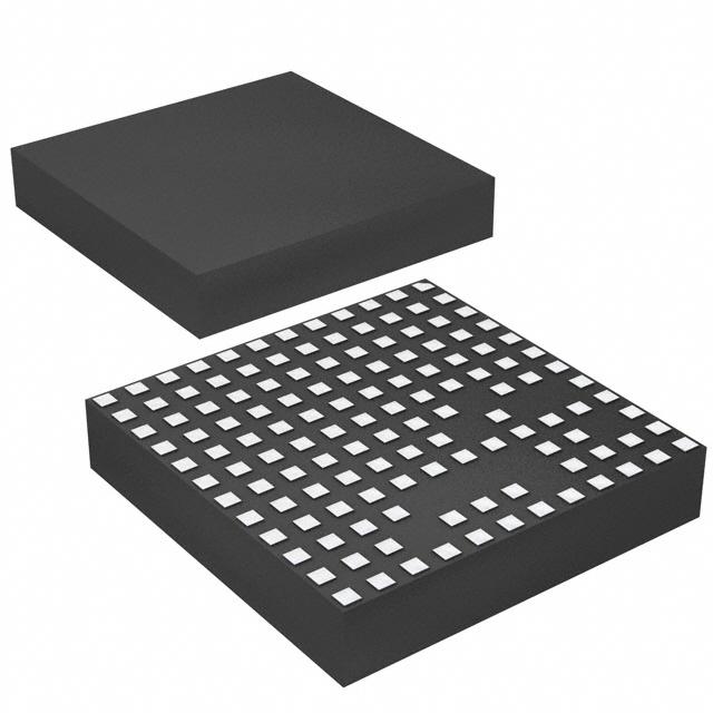
PACKAGE PHOTOGRAPH
2.82mm
15mm
15mm
3.42mm
15mm
15mm
RELATED PARTS
PART NUMBER DESCRIPTION
COMMENTS
LTM4601/
LTM4601A
12A DC/DC µModule Regulator with PLL, Output
Tracking/Margining and Remote Sensing
Synchronizable, PolyPhase Operation, LTM4601-1/LTM4601A-1 Version Has No
Remote Sensing, LGA Package
LTM4618
6A DC/DC µModule Regulator with PLL,
Output Tracking
4.5V ≤ VIN ≤ 26.5V, 0.8V ≤ VOUT ≤ 5V, Synchronizable, 9mm × 15mm × 4.3mm
LGA Package
LTM4604A
Low VIN 4A DC/DC µModule Regulator
2.375V ≤ VIN ≤ 5.5V, 0.8V ≤ VOUT ≤ 5V, 9mm × 15mm × 2.3mm LGA Package
LTM4608A
Low VIN 8A DC/DC µModule Regulator
2.375V ≤ VIN ≤ 5.5V, 0.6V ≤ VOUT ≤ 5V, 9mm × 15mm × 2.8mm LGA Package
LTM4612
Low Noise 5A, 15VOUT DC/DC µModule Regulator
Low Noise, with PLL, Output Tracking and Margining, LTM4606 Pin-Compatible
LTM4613
Low Noise 8A, 15VOUT DC/DC µModule Regulator
Low Noise, with PLL, Output Tracking and Margining, EN55022B Compliant
LTM4627
15A DC/DC µModule Regulator
4.5V ≤ VIN ≤ 20V, 0.6V ≤ VOUT ≤ 5V, ±1.5% Total DC Output Accuracy,
15mm × 15mm × 4.32mm LGA Package
EN55022 Class B Certified DC/DC µModule Regulators
LTM8020
High VIN 0.2A DC/DC Step-Down µModule Regulator
4V ≤ VIN ≤ 36V, 1.25V ≤ VOUT ≤ 5V, 6.25mm × 6.25mm × 2.3mm LGA Package
LTM8021
High VIN 0.5A DC/DC Step-Down µModule Regulator
3V ≤ VIN ≤ 36V, 0.8V ≤ VOUT ≤ 5V, 6.25mm × 11.25mm × 2.8mm LGA Package
LTM8022/
LTM8023
36VIN, 1A and 2A DC/DC µModule Regulators
Pin Compatible, 4.5V ≤ VIN ≤ 36V, 9mm × 11.25mm × 2.8mm LGA Package
LTM8031/
LTM8032
1A, 2A EMC DC/DC µModule Regulators
EN55022 Class B Compliant, 3.6V ≤ VIN ≤ 36V, 0.8V ≤ VOUT ≤ 10V,
Pin Compatible, 9mm × 15mm × 2.82mm LGA Package
LTM8033
3A EMC DC/DC µModule Regulator
3.6V ≤ VIN ≤ 36V, 0.8V ≤ VOUT ≤ 24V, 11.25mm × 15mm × 4.32mm LGA
Package
28
Rev. E
06/21
www.analog.com
For more information www.analog.com
ANALOG DEVICES, INC. 2008-2021
�