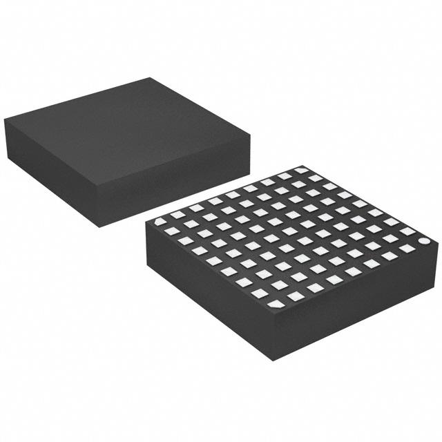
LTM9001-GA
16-Bit IF/Baseband
Receiver Subsystem
FEATURES
DESCRIPTION
n
The LTM®9001 is an integrated System in a Package (SiP)
that includes a high-speed 16-bit A/D converter, matching
network, anti-aliasing filter and a low noise, differential
amplifier with fixed gain. It is designed for digitizing wide
dynamic range signals with an intermediate frequency (IF)
range up to 300MHz. The amplifier allows either AC- or DCcoupled input drive. A lowpass or bandpass filter network
can be implemented with various bandwidths. Contact
Linear Technology regarding semi-custom configurations,
(see Table 1.)
n
n
n
n
n
n
n
n
n
n
Integrated 16-Bit, High-Speed ADC, Passive Filter
and Fixed Gain Differential Amplifier
Up to 300MHz IF Range
Lowpass and Bandpass Filter Versions
Low Noise, Low Distortion Amplifiers
Fixed Gain: 8dB, 14dB, 20dB or 26dB
50Ω, 200Ω or 400Ω Input Impedance
78dB SNR, 87dB SFDR (LTM9001-GA)
Integrated Bypass Capacitance, No External
Components Required
Optional Internal Dither
Optional Data Output Randomizer
3.3V Single Supply
Power Dissipation: 550mW (LTM9001-GA)
Clock Duty Cycle Stabilizer
11.25mm × 11.25mm × 2.32mm LGA Package
APPLICATIONS
n
n
n
n
n
The LTM9001 is perfect for IF receivers in demanding
communications applications, with AC performance that
includes 78dBFS noise floor and 87dB spurious free
dynamic range (SFDR) at 5MHz (LTM9001-GA).
The digital outputs are single-ended CMOS. A separate
output power supply allows the CMOS output swing to
range from 0.5V to 3.3V.
An optional clock duty cycle stabilizer allows high performance at full speed with a wide range of clock duty cycles.
Telecommunications
High Sensitivity Receivers
Imaging Systems
Spectrum Analyzers
ATE
L, LT, LTC, LTM, Linear Technology and the Linear logo are registered trademarks of Linear
Technology Corporation. All other trademarks are the property of their respective owners.
TYPICAL APPLICATION
Simplified IF Receiver Channel
SENSE
VDD = 3.3V
LTM9001-GA
0VDD =
0.5V TO 3.6V
D15
IN–
RF
ANTI-ALIAS
FILTER
SAW
LO
16-BIT
25Msps ADC
IN+
•
•
•
D0
CLKOUT
OF
DIFFERENTIAL
FIXED GAIN
AMPLIFIER
OGND
9001-GA TA01
GND
CLK
AMPLITUDE (dBFS)
VCC
64k Point FFT, fIN = 5MHz,
–1dBFS, PGA = 0
0
–10
–20
–30
–40
–50
–60
–70
–80
–90
–100
–110
–120
–130
LTM9001-GA
HD2
0.0
2.5
HD3
5.0
7.5
10.0
FREQUENCY (MHz)
12.5
9001-GA TA01a
ADC CONTROL PINS
9001gaf
1
�LTM9001-GA
ABSOLUTE MAXIMUM RATINGS
PIN CONFIGURATION
(Notes 1, 2)
Supply Voltage (VCC) ................................ –0.3V to 3.6V
Supply Voltage (VDD) ................................... –0.3V to 4V
Digital Output Supply Voltage (OVDD) .......... –0.3V to 4V
Analog Input Current (IN+, IN–) ............................±10mA
Digital Input Voltage
(Except AMPSHDN) ................. –0.3V to (VDD + 0.3V)
Digital Input Voltage
(AMPSHDN)..............................–0.3V to (VCC + 0.3V)
Digital Output Voltage ................–0.3V to (OVDD + 0.3V)
Operating Temperature Range
LTM9001C................................................ 0°C to 70°C
LTM9001I.............................................–40°C to 85°C
Storage Temperature Range...................–45°C to 125°C
Maximum Junction Temperature........................... 125°C
ALL ELSE
= GND
TOP VIEW
CONTROL
1
2
DATA
3
4
5
6
7
8
9
OGND
J
IN–
H
IN+
G
OVDD
F
VCC E
DNC D
C
CLK B
A
OGND
VDD OGND OVDD
CONTROL
LGA PACKAGE
TJMAX = 125°C, QJA = 15°C/W, QJC = 19°C/W
QJA DERIVED FROM 60mm s 70mm PCB WITH 4 LAYERS
WEIGHT = 0.71g
ORDER INFORMATION
LEAD FREE FINISH
TRAY
PART MARKING* PACKAGE DESCRIPTION
TEMPERATURE RANGE
LTM9001CV-GA#PBF
LTM9001CV-GA#PBF
LTM9001V-GA
81-Lead (11.25mm × 11.25mm × 2.3mm) LGA
0°C to 70°C
LTM9001IV-GA#PBF
LTM9001IV-GA#PBF
LTM9001V-GA
81-Lead (11.25mm × 11.25mm × 2.3mm) LGA
–40°C to 85°C
Consult LTC Marketing for parts specified with wider operating temperature ranges. *The temperature grade is identified by a label on the shipping container.
Consult LTC Marketing for information on non-standard lead based finish parts.
For more information on lead free part marking, go to: http://www.linear.com/leadfree/
This product is only offered in trays. For more information go to: http://www.linear.com/packaging/
ELECTRICAL CHARACTERISTICS
The l denotes the specifications which apply over the full operating
temperature range, otherwise specifications are at TA = 25°C. (Note 4)
SYMBOL
PARAMETER
CONDITIONS
GDIFF
Gain
DC, LTM9001-GA
fIN = 5MHz
GTEMP
Gain Temperature Drift
VIN = Maximum, (Note 3)
VINCM
Input Common Mode Voltage Range
(IN+ + IN–)/2
VIN
Input Voltage Range at –1dBFS
LTM9001-GA at 5MHz
900
RINDIFF
Differential Input Impedance
LTM9001-GA
400
Ω
CINDIFF
Differential Input Capacitance
Includes Parasitic
1
pF
VOS
Offset Error (Note 6)
Including Amplifier and ADC (LTM9001-GA)
–10
mV
l
MIN
TYP
MAX
7.2
8
8
8.8
2
1.0–1.6
l
–50
UNITS
dB
mdB/°C
V
mVP-P
Offset Drift
Including Amplifier and ADC
±10
μV/°C
Full-Scale Drift
Internal Reference
External Reference
±30
±15
ppm/°C
ppm/°C
9001gaf
2
�LTM9001-GA
ELECTRICAL CHARACTERISTICS
The l denotes the specifications which apply over the full operating
temperature range, otherwise specifications are at TA = 25°C. (Note 4)
SYMBOL
PARAMETER
CMRR
Common Mode Rejection Ratio
CONDITIONS
MIN
TYP
MAX
UNITS
60
0V < SENSE < VDD (Note 9)
l
–3
dB
ISENSE
SENSE Input Leakage Current
IMODE
MODE Pin Pull-Down Current to GND
10
3
μA
μA
IOE
OE Pin Pull-Down Current to GND
10
μA
tAP
Sample-and-Hold Acquisition Delay Time
1
ns
tJITTER
Sample-and-Hold Acquisition Delay Time Jitter
70
fsRMS
CONVERTER CHARACTERISTICS
The l indicates specifications which apply over the full operating
temperature range, otherwise specifications are at TA = 25°C.
PARAMETER
CONDITIONS
MIN
l
Resolution (No Missing Codes)
TYP
MAX
16
Bits
Differential Input LTM9001-GA (Note 5)
l
±2.4
±8
Differential Linearity Error
Differential Input
l
±0.3
±1
Transition Noise
External Reference
Integral Linearity Error
UNITS
1
LSB
LSB
LSBRMS
DYNAMIC ACCURACY
The l indicates specifications which apply over the full operating temperature range,
otherwise specifications are at TA = 25°C. AIN = –1dBFS. (Note 4)
SYMBOL
PARAMETER
CONDITIONS
MIN
TYP
SNR
Signal-to-Noise Ratio
5MHz Input (PGA = 0)
5MHz Input (PGA = 1)
SFDR
Spurious Free Dynamic Range, 2nd or 3rd
Harmonic
SFDR
MAX
UNITS
l
76
78
75.4
dBFS
dBFS
5MHz Input (PGA = 0)
5MHz Input (PGA = 1)
l
76
87
89.8
dBc
dBc
Spurious Free Dynamic Range 4th or Higher
5MHz Input (PGA = 0)
5MHz Input (PGA = 1)
l
91
100
99
dBc
dBc
S/(N+D)
Signal-to-Noise Plus Distortion Ratio
5MHz Input (PGA = 0)
5MHz Input (PGA = 1)
l
75
77.4
74.8
dBFS
dBFS
SFDR
Spurious Free Dynamic Range at –15dBFS,
Dither “OFF”
5MHz Input (PGA = 0)
5MHz Input (PGA = 1)
l
91
105
107.5
dBFS
dBFS
SFDR
Spurious Free Dynamic Range at –15dBFS,
Dither “ON”
5MHz Input (PGA = 0)
5MHz Input (PGA = 1)
l
93
107
109
dBFS
dBFS
IMD3
Third Order Intermodulation Distortion;
1MHz Tone Spacing, 2 Tones at –7dBFS
fIN = 5MHz
85
dB
IIP3
Equivalent Third Order Input Intercept Point,
2 Tone
fIN = 5MHz
36.5
dBm
9001gaf
3
�LTM9001-GA
DIGITAL INPUTS AND OUTPUTS
The l denotes the specifications which apply over the full operating
temperature range, otherwise specifications are at TA = 25°C. (Note 4)
SYMBOL
PARAMETER
CONDITIONS
MIN
TYP
MAX
UNITS
Logic Inputs (DITH, PGA, ADCSHDN, RAND, CLK, OE)
VDD = 3.3V
l
Low Level Input Voltage
VDD = 3.3V
l
0.8
V
Input Current
VIN = 0V to VDD
l
±10
μA
Input Capacitance
(Note 7)
VIH
High Level Input Voltage
VIL
IIN
CIN
2
V
1.5
pF
Logic Inputs (AMPSHDN)
VCC = 3.3V
l
Low Level Input Voltage
VCC = 3.3V
l
Input High Current
VIN = 2V
1.3
μA
IIL
Input Low Current
VIN = 0.8V
0.1
μA
CIN
Input Capacitance
(Note 7)
1.5
pF
High Level Output Voltage
VDD = 3.3V, IO = –10μA
VDD = 3.3V, IO = –200μA
l
3.299
3.29
V
V
VDD = 3.3V, IO = 10μA
VDD = 3.3V, IO = 1.6mA
l
VIH
High Level Input Voltage
VIL
IIH
2
V
0.8
V
Logic Outputs
OVDD = 3.3V
VOH
VOL
Low Level Output Voltage
3.1
0.01
0.1
V
V
0.4
ISOURCE
Output Source Current
VOUT = 0V
–50
mA
ISINK
Output Sink Current
VOUT = 3.3V
50
mA
VOH
High Level Output Voltage
VDD = 3.3V, IO = –200μA
2.49
V
VOL
Low Level Output Voltage
VDD = 3.3V, IO = 1.6mA
0.1
V
VOH
High Level Output Voltage
VDD = 3.3V, IO = –200μA
1.79
V
VOL
Low Level Output Voltage
VDD = 3.3V, IO = 1.6μA
0.1
V
OVDD = 2.5V
OVDD = 1.8V
POWER REQUIREMENTS
The l denotes the specifications which apply over the full operating temperature
range, otherwise specifications are at TA = 25°C. (Note 4)
SYMBOL
PARAMETER
CONDITIONS
VDD
ADC Analog Supply Voltage
(Note 8)
MIN
TYP
MAX
UNITS
l
3.135
3.3
3.465
V
2.85
3.5
V
100
136
mA
VCC
Amplifier Supply Voltage
l
ICC
Amplifier Supply Current
l
PSHDN
Total Shutdown Power
AMPSHDN = ADCSHDN = 3.3V
OVDD
Output Supply Voltage
(Note 8)
l
10
0.5
mW
3.6
V
IVDD
Analog Supply Current
LTM9001-GA
l
66
80
mA
PDISS
ADC Power Dissipation
LTM9001-GA
l
220
265
mW
PDISS(TOTAL)
Total Power Dissipation
LTM9001-GA
550
mW
9001gaf
4
�LTM9001-GA
TIMING CHARACTERISTICS
The l denotes the specifications which apply over the full operating temperature
range, otherwise specifications are at TA = 25°C. (Note 4)
SYMBOL
PARAMETER
CONDITIONS
MIN
fS
Sampling Frequency (Note 8)
LTM9001-GA
l
1
tL
CLK Low Time (Note 7)
Duty Cycle Stabilizer Off
Duty Cycle Stabilizer On
l
l
18.9
5
tH
CLK High Time (Note 7)
Duty Cycle Stabilizer Off
Duty Cycle Stabilizer On
l
l
tD
CLK to DATA Delay
(Note 7)
tC
CLK to CLKOUT Delay
tSKEW
DATA to CLKOUT Skew
TYP
MAX
UNITS
25
MHz
20
20
500
500
ns
ns
18.9
5
20
20
500
500
ns
ns
l
1.3
3.1
4.9
ns
(Note 7)
l
1.3
3.1
4.9
ns
(tC – tD) (Note 7)
l
–0.6
0
0.6
CMOS Output Mode
Data Latency
Note 1: Stresses beyond those listed under Absolute Maximum Ratings
may cause permanent damage to the device. Exposure to any Absolute
Maximum Rating condition for extended periods may affect device
reliability and lifetime.
Note 2: All voltage values are with respect to ground with GND and OGND
wired together (unless otherwise noted).
Note 3: Gain is measured from IN+/IN– through the ADC.
Note 4: VCC = VDD = 3.3V, fSAMPLE = maximum sample frequency, input
range = –1dBFS with PGA = 0 with differential drive, AC-coupled inputs,
unless otherwise noted.
7
ns
Cycles
Note 5: Integral nonlinearity is defined as the deviation of a code from
a “best fit straight line” to the transfer curve. The deviation is measured
from the center of the quantization band.
Note 6: Offset error is the voltage applied between the IN+ and IN– pins
required to make the output code flicker between 0000 0000 0000 0000
and 1111 1111 1111 1111.
Note 7: Guaranteed by design, not subject to test.
Note 8: Recommended operating conditions.
Note 9: Leakage current will experience transient at power up. Keep
resistance