Matched Monolithic
Dual Transistor
MAT01
Data Sheet
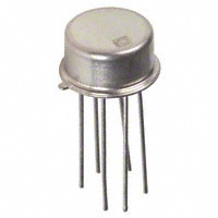
PIN CONNECTION DIAGRAM
Low VOS (VBE match): 40 µV typical, 100 µV maximum
Low TCVOS: 0.5 µV/°C maximum
High hFE: 500 minimum
Excellent hFE linearity from 10 nA to 10 mA
Low noise voltage: 0.23 µV p-p from 0.1 Hz to 10 Hz
High breakdown: 45 V min
APPLICATIONS
MAT01
TOP VIEW
(Not to Scale)
C1
1
6
5 B2
B1 2
4 E
2
E1 3
Weigh scales
Low noise, op amp, front end
Current mirror and current sink/source
Low noise instrumentation amplifiers
Voltage controlled attenuators
Log amplifiers
C2
NOTES
1. SUBSTRATE IS CONNECTED TO CASE.
00282-001
FEATURES
Figure 1.
GENERAL DESCRIPTION
The MAT01 is a monolithic dual NPN transistor. An exclusive
silicon nitride triple passivation process provides excellent
stability of critical parameters over both temperature and time.
Matching characteristics include offset voltage of 40 µV,
temperature drift of 0.15 µV/°C, and hFE matching of 0.7%.
Rev. D
High hFE is provided over a six decade range of collector
current, including an exceptional hFE of 590 at a collector
current of only 10 nA. The high gain at low collector current
makes the MAT01 ideal for use in low power, low level input
stages.
Document Feedback
Information furnished by Analog Devices is believed to be accurate and reliable. However, no
responsibility is assumed by Analog Devices for its use, nor for any infringements of patents or other
rights of third parties that may result from its use. Specifications subject to change without notice. No
license is granted by implication or otherwise under any patent or patent rights of Analog Devices.
Trademarks and registered trademarks are the property of their respective owners.
One Technology Way, P.O. Box 9106, Norwood, MA 02062-9106, U.S.A.
Tel: 781.329.4700 ©1973–2014 Analog Devices, Inc. All rights reserved.
Technical Support
www.analog.com
�MAT01
Data Sheet
TABLE OF CONTENTS
Features .............................................................................................. 1
ESD Caution...................................................................................5
Applications ....................................................................................... 1
Typical Performance Characteristics ..............................................6
Pin Connection Diagram ................................................................ 1
Test Circuits........................................................................................8
General Description ......................................................................... 1
Applications Information .................................................................9
Revision History ............................................................................... 2
Typical Applications ....................................................................... 10
Specifications..................................................................................... 3
Outline Dimensions ....................................................................... 11
Electrical Characteristics ............................................................. 3
Ordering Guide .......................................................................... 11
Absolute Maximum Ratings ............................................................ 5
REVISION HISTORY
9/14—Rev. C to Rev. D
2/02—Rev. A to Rev. B
Changes to Figure 4 and Figure 7 ................................................... 6
Edits to Features.................................................................................1
Deleted Wafer Test Limits ................................................................3
Deleted DICE Characteristics ..........................................................3
Edits to Table 5 ...................................................................................7
4/13—Rev. B to Rev. C
Updated Format .................................................................. Universal
Added Applications Section, Deleted Figure 2,
Renumbered Sequentially................................................................ 1
Deleted Table 3, Renumbered Sequentially................................... 4
Changes to Table 3 ............................................................................ 5
Changes to Typical Performance Characteristics Section ........... 6
Updated Outline Dimensions ....................................................... 11
Changes to Ordering Guide .......................................................... 11
Rev. D | Page 2 of 12
�Data Sheet
MAT01
SPECIFICATIONS
ELECTRICAL CHARACTERISTICS
VCB = 15 V, IC = 10 µA, TA = 25°C, unless otherwise noted.
Table 1.
Parameter
VOLTAGE
Breakdown Voltage
Offset Voltage
Offset Voltage Stability
First Month1
Long Term2
CURRENT
Offset Current
Bias Current
Current Gain
Current Gain Match
NOISE
Low Frequency Noise Voltage
Broadband Noise Voltage
Noise Voltage Density
OFFSET VOLTAGE/CURRENT
Offset Voltage Change
Offset Current Change
LEAKAGE
Collector to Base Leakage Current
Collector to Emitter Leakage Current
Collector to Collector Leakage Current
SATURATION
Collector Saturation Voltage
GAIN BANDWIDTH PRODUCT
CAPACITANCE
Output Capacitance
Collector to Collector Capacitance
Symbol
Test Conditions/Comments
Min
BVCEO
VOS
IC = 100 µA
45
MAT01AH
Typ Max
0.1
VOS/Time
2.0
0.2
IOS
IB
hFE
0.1
13
590
770
840
0.7
0.8
0.6
20
∆hFE
500
MAT01GH
Typ Min
45
0.04
IC = 10 nA
IC = 10 µA
IC = 10 mA
IC = 10 µA
100 nA ≤ IC ≤ 10 mA
Min
0.10
0.5
2.0
0.2
250
3.0
Unit
V
mV
µV/Mo
µV/Mo
0.2
18
430
560
610
1.0
1.2
3.2
40
nA
nA
8.0
%
%
0.4
9.0
7.6
7.5
µV p-p
µV rms
nV/√Hz
nV/√Hz
nV/√Hz
en p-p
en rms
en
0.1 Hz to 10 Hz3
1 Hz to 10 kHz
fO = 10 Hz3
fO = 100 Hz3
fO = 1000 Hz3
0.23
0.60
7.0
6.1
6.0
0.4
9.0
7.6
7.5
0.23
0.60
7.0
6.1
6.0
∆VOS/∆VCB
∆IOS/∆VCB
0 ≤ VCB ≤ 30 V
0 ≤ VCB ≤ 30 V
0.5
2
3.0
15
0.8
3
8.0
70
µV/V
pA/V
ICBO
ICES
ICC
VCB = 30 V, IE = 04
VCE = 30 V, VBE = 04, 5
VCC = 30 V5
15
50
20
50
200
200
25
90
30
200
400
400
pA
pA
pA
VCE(SAT)
0.12
0.8
450
0.20
0.12
0.8
450
0.25
fT
IB = 0.1 mA, IC = 1 mA
IB = 1 mA, IC = 10 mA
VCE = 10 V, IC = 10 mA
V
V
MHz
COB
CCC
VCB = 15 V, IE = 0
VCC = 0
2.8
8.5
1
2.8
8.5
pF
pF
Exclude first hour of operation to allow for stabilization.
Parameter describes long-term average drift after first month of operation.
3
Sample tested.
4
The collector to base (ICBO) and collector to emitter (ICES) leakage currents can be reduced by a factor of 2 to 10 times by connecting the substrate (package) to a
potential that is lower than either collector voltage.
5
ICC and ICES are guaranteed by measurement of ICBO.
2
Rev. D | Page 3 of 12
�MAT01
Data Sheet
VCB = 15 V, IC = 10 µA, −55°C ≤ TA ≤ +125°C, unless otherwise noted.
Table 2.
Parameter
OFFSET VOLTAGE/CURRENT
Offset Voltage
Average Offset Voltage Drift1
Offset Current
Average Offset Current Drift2
BIAS CURRENT
CURRENT GAIN
LEAKAGE CURRENT
Collector to Base Leakage Current
Collector to Emitter Leakage Current
Collector to Collector Leakage Current
(
Symbol
Test Conditions/Comments
VOS
TCVOS
IOS
TCIOS
ΙΒ
hFE
ICBO
ICES
ICC
Min
167
TA = 125°C, VCB = 30 V, IE = 03
TA = 125°C, VCE = 30 V, VBE = 01, 3
TA = 125°C, VCC = 30 V1
)
MAT01AH
Typ Max
0.06
0.15
0.9
10
28
400
0.15
0.50
8.0
90
60
15
50
30
80
300
200
Min
77
MAT01GH
Typ Min
0.14
0.35
1.5
15
36
300
0.70
1.8
15.0
150
130
mV
µV/°C
nA
pA/°C
nA
25
90
50
200
400
400
nA
nA
nA
V
Guaranteed by VOS test TCVOS ≅ OS for VOS
很抱歉,暂时无法提供与“MAT01GHZ”相匹配的价格&库存,您可以联系我们找货
免费人工找货