19-1291; Rev 0; 9/97
IF Undersampler
The MAX1005 provides a high level of signal integrity
from a low power budget. It operates from a single
power supply, or from separate analog and digital supplies with independent voltages ranging from +2.7V to
+5.5V. The MAX1005 can operate with an unregulated
analog supply of 5.5V and a regulated digital supply
down to 2.7V. This flexible power-supply operation
saves additional power in complex digital systems.
The MAX1005 has three operating modes: transmit
(DAC active), receive (ADC active), and shutdown
(ADC and DAC inactive). In shutdown mode, the total
supply current drops below 1µA. The device requires
only 2.4µs to wake up from shutdown mode. The
MAX1005 is ideal for hand-held, as well as base-station
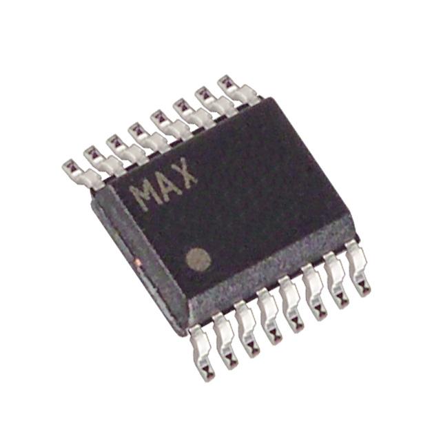
applications. It is available in a tiny 16-pin QSOP package specified for operation over both the commercial
and extended temperature ranges.
________________________Applications
____________________________Features
♦ Differential-Input, 5-Bit ADC
♦ Differential-Output, 7-Bit DAC
♦ 15Msps Min Conversion Rate
♦ 25MHz -1dB Full-Power Bandwidth
♦ 44dB SFDR for ADC
39dB at 10.7MHz SFDR (Imaged) for DAC
♦ Internal Voltage Reference
♦ Parallel Logic Interface
♦ Single-Supply Operation (+2.7V to +5.5V)
♦ 0.1µA Low-Power Shutdown Mode
______________Ordering Information
PART
MAX1005CEE
MAX1005EEE
TEMP. RANGE
PIN-PACKAGE
0°C to +70°C
-40°C to +85°C
16 QSOP
16 QSOP
__________________Pin Configuration
TOP VIEW
VCCD 1
16 CLK
DGND 2
15 D0
RXEN 3
14 D1
PWT1900
AIO+ 4
PHS/P
AIO- 5
12 D3
Wireless Loops
TXEN 6
11 D4
PCS/N
AGND 7
10 D5
VCCA 8
9
MAX1005
13 D2
D6
QSOP
Functional Diagram appears at end of data sheet.
________________________________________________________________ Maxim Integrated Products
1
For free samples & the latest literature: http://www.maxim-ic.com, or phone 1-800-998-8800.
For small orders, phone 408-737-7600 ext. 3468.
MAX1005
_______________General Description
The MAX1005 is a combined digitizer and reconstruction integrated circuit designed to work in systems that
demodulate and modulate communications signals. It
integrates IF undersampling and signal synthesis functions into a single, low-power circuit. Its analog-todigital converter (ADC) is used to directly sample or
undersample a downconverted RF signal, while its
digital-to-analog converter (DAC) recreates the IF subcarrier and transmission data. The MAX1005’s ADC is
ideal for undersampling applications, due to the analog
input amplifier’s wide (15MHz) bandwidth. The DAC
has very low glitch energy, which minimizes the transmission of unwanted spurious signals. An on-chip
reference provides for low-noise ADC and DAC conversions.
�MAX1005
IF Undersampler
ABSOLUTE MAXIMUM RATINGS
VCCA to AGND ........................................................-0.3V, +6.0V
VCCD to DGND ........................................................-0.3V, +6.0V
VCCA to VCCD ...................................................................±6.3V
Digital I/O Pins (D0–D6, CLK, RXEN, TXEN)
to DGND .................................-0.3V to (VCCD + 0.3V) or 6.0V
(whichever is smaller)
Analog I/O Pins (AIO+, AIO-)
to AGND................................(VCCA - 1.5V) to (VCCA + 0.3V)
AGND to DGND........................................................-0.3V, +0.3V
Power Dissipation (TA = +70°C)
QSOP (derate 5.90mW/°C above 70°C) ......................470mW
Operating Temperature Ranges
MAX1005CEE .....................................................0°C to +70°C
MAX1005EEE...................................................-40°C to +85°C
Storage Temperature Range .............................-65°C to +150°C
Lead Temperature (soldering,
很抱歉,暂时无法提供与“MAX1005EEE+”相匹配的价格&库存,您可以联系我们找货
免费人工找货