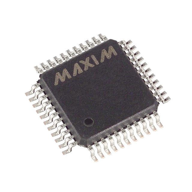
MAX136
Low Power, 31⁄2 Digit A/D Converter
with Display Hold
General Description
Features
The MAX136 is a monolithic analog-to-digital converter
(ADC) with very high input impedance. It differs from the
Maxim ICL7136 in that the MAX136 provides a Hold pin,
which makes it possible to hold or "freeze" a reading. The
MAX136 directly drives a nonmultiplexed liquid crystal
(LCD) display, requiring no external drive circuitry. With
minor external component changes, it is pin compatible
with the ICL7116 but with significantly reduced power
consumption, making the MAX136 a superior device for
portable systems.
• Power Dissipation Guaranteed Less than 1mW–9V
Battery Life 3000 Hours Typical
Versatility and accuracy are inherent features of this
ADC. The dual-slope conversion technique automatically
rejects interference signals common in industrial environments. True differential inputs allow direct measurements of bridge transducer outputs or load cells. The
zero-integrator phase eliminates overrange hangover
and hysteresis effects. The MAX136 offers high accuracy
by lowering rollover error to less than one count and zero
reading drift to less than 1µV/°C.
Applications
These devices can be used in a wide range of digital
panel meter applications. Most applications, however,
involve the measurement and display of analog data:
Pressure
Voltage
Resistance
Temperature
Conductance
Current
Speed
Material Thickness
• Hold Pin Allows Indefinite Display Hold
• Guaranteed First Reading Recovery from
Overrange
• On-Board Display Drive Capability—No External
Circuitry Required
• High-Impedance CMOS Differential Inputs
• Low Noise(< 15µVP-P) Without Hysteresis or
Overrange Hangover
• Clock and Reference On-Chip
• Zero Input Gives Zero Reading
• True Polarity Indication for Precision Null
Applications
• Key Parameters Guaranteed Over Temperature
Ordering Information
PART
TEMP RANGE
PIN-PACKAGE
MAX136CPL+
0°C to +70°C
40 PDIP
MAX136CMH+
0°C to +70°C
44 MQFP
MAX136CQH+
0°C to +70°C
44 PLCC
MAX136C/D
0°C to +70°C
Dice
+Denotes a lead(Pb)-free/RoHS-compliant package.
Pin Configurations
Typical Operating Circuit
LCD DISPLAY
ANALOG
INPUT
MAX136
9V
VREF
TO ANALOG
COMMON (P32)
(Detailed Circuit Diagram—See 3rd page)
Pin Configurations continued at end of data sheet
For pricing, delivery, and ordering information, please contact Maxim Direct at
1-888-629-4642, or visit Maxim Integrated’s website at www.maximintegrated.com.
19-0890; Rev 1; 11/12
�MAX136
Low Power, 31⁄2 Digit A/D Converter
with Display Hold
ABSOLUTE MAXIMUM RATINGS
Supply Voltage (V+ to V-)......................................................15V
Analog Input Voltage (either input) (Note 1)...................V+ to VReference Input Voltage (either input)............................V+ to VClock Input, Hold Input..............................................TEST to V+
Power Dissipation (Note 2)
PDIP..............................................................................800mW
Operating Temperature Range.............................. 0°C to +70°C
Storage Temperature........................................ -65°C to +160°C
Lead Temperature (soldering, 60s).................................+300°C
Note 1: Input voltages may exceed the supply voltages, provided the input current is limited to ±1mA.
Note 2: Dissipation rating assumes device is mounted with all leads soldered to printed circuit board.
2
Maxim Integrated
�MAX136
Low Power, 31⁄2 Digit A/D Converter
with Display Hold
Detailed Description
The MAX136 3½ digit ADC is similar to the Maxim
ICL7136 except for the addition of a Hold pin. For a
detailed product description, and applications information (other than the operation of the Hold pin described
below), refer to Maxim's ICL7136 data sheet.
Hold Input
The Hold input is a digital input with a logic threshold approximately midway between V+ and Test. The
MAX136 continuously performs conversions, independent of the Hold input. When the Hold input is at V+ the
display latch pulse is inhibited, and the display latches
are not updated; when the Hold input is low or at the
Test voltage, the display is updated at the end of each
conversion. The MAX136 maintains low-power dissipation even during display hold by eliminating the pulldown
resistor between Hold and Test present on the ICL7116.
The Hold input is CMOS compatible, and can also be
driven by a switch connected between Test and V+
(Figure 1).
Reference Input
Unlike the ICL7136, the MAX136 does not have a reference low input. Apply the reference voltage between
Reference High (REF HI) and
0.47µF
0.47µF
34
33
LCD DISPLAY
C+ REF C- REF
2-19 SEGMENT
22-25 DRIVE
31
IN HI
PDL 20
BACKPLANE
BP 21 MINUS SIGN DRIVE
30
TEST 37
RUN
IN LO
1
32
HOLD
COMMON
HOLD
35
28
V+
BUFF
1MI
ANALOG
INPUT
0.01µF
180kI
0.47µF
29
0.047µF
27
A/Z
REF HI
INT
VREF
36
OSC2 OSC3 OSC1
38 COSC 40
100kI
TO ANALOG
COMMON (P32)
0.047µF
0.47µF
29
27
150kI
MAX136
A/Z
VREF
36
REF HI
INT
9V
100kI
26
V-
OSC2 OSC3 OSC1
38 COSC 40
39
TO ANALOG
COMMON (P32)
ROSC
ROSC
50pF
180kI
Figure 1. MAX136 Typical Operating Circuit, 200mV Full Scale
Maxim Integrated
0.01µF
9V
26
V-
39
ANALOG
INPUT
180kI
150kI
MAX136
1MI
34
33
LCD DISPLAY
C+ REF C- REF
2-19 SEGMENT
22-25 DRIVE
31
IN HI
PDL 20
BACKPLANE
BP 21 MINUS SIGN DRIVE
37
30
TEST
RUN
IN LO
1
32
HOLD
COMMON
HOLD
35
28
V+
BUFF
50pF
180kI
Figure 2. MAX136 Typical Operating Circuit, 2.0V Full Scale
3
�MAX136
Low Power, 31⁄2 Digit A/D Converter
with Display Hold
Pin Configurations (continued)
C2
11
35 IN HI
N.C.
12
B2
13
A2
MAX136
34 N.C.
33 IN LO
32 A/Z
14
31 BUFF
E2
16
30 INT
D3
17
29 V−
G2
C3
A3
G3
BP
N.C.
AB4
POL
19 20 21 22 23 24 25 26 27 28
E3
18
F3
15
B3
F2
34
35
36
37
38
39
40
41
3
31
4
30
5
29
MAX136
6
28
7
27
8
26
9
25
10
24
11
23
N.C.
G2(TENS)
C3
A3
G3
BP
POL(-)
AB4
E3
F3
B3
22
36 COMMON
21
10
20
D2
32
19
37 C-REF
33
2
18
9
1
17
E1
N.C.
N.C.
TEST
OSC3
N.C.
OSC2
OSC1
HOLD
D1
C1
B1
16
38 C+REF
15
8
14
G1
42
REF HI
V+
C+REF
C-REF
COMMON
INHI
INLO
A/Z
BUFF
INT
V39 V+
12
7
A1
F1
G1
E1
D2
C2
B2
A2
F2
E2
D3
F1
43
44
44 43 42 41 40
13
1
REF HI
2
TEST
N.C.
3
OSC3
HOLD
4
OSC2
D1
5
OSC1
B1
6
C1
A1
TOP VIEW
PLCC
MQFP
Package Information
For the latest package outline information and land patterns (footprints), go to www.maximintegrated.com/packages. Note that a
“+”, “#”, or “-” in the package code indicates RoHS status only. Package drawings may show a different suffix character, but the
drawing pertains to the package regardless of RoHS status.
PART TYPE
4
PACKAGE CODE
DOCUMENT NO.
LAND PATTERN No.
40 PDIP
P40+1
21-0044
—
44 PLCC
Q44+1
21-0049
90-0236
44 MQFP
M44+5
21-0826
90-0169
Maxim Integrated
�MAX136
Low Power, 31⁄2 Digit A/D Converter
with Display Hold
Revision History
REVISION
NUMBER
REVISION
DATE
DESCRIPTION
0
2/87
Initial release
1
11/12
Add MQFP package to Ordering Information and Package Information.
PAGES
CHANGED
—
1, 4
Maxim Integrated cannot assume responsibility for use of any circuitry other than circuitry entirely embodied in a Maxim Integrated product. No circuit patent
licenses are implied. Maxim Integrated reserves the right to change the circuitry and specifications without notice at any time. The parametric values (min and
max limits) shown in the Electrical Characteristics table are guaranteed. Other parametric values quoted in this data sheet are provided for guidance.
Maxim Integrated 160 Rio Robles, San Jose, CA 95134 USA 1-408-601-1000�
© 2012
Maxim Integrated Products, Inc.�
5
Maxim Integrated and the Maxim Integrated logo are trademarks of Maxim Integrated Products, Inc.
�
很抱歉,暂时无法提供与“MAX136CMH+TD”相匹配的价格&库存,您可以联系我们找货
免费人工找货