EVALUATION KIT AVAILABLE
MAX16815/MAX16828
High-Voltage, 100mA/200mA Adjustable Linear
High-Brightness LED Drivers with PWM Dimming
General Description
The MAX16815/MAX16828 current regulators operate
from a 6.5V to 40V input voltage range and deliver
up to 100mA (MAX16815) or 200mA (MAX16828) to
high-brightness LED (HB LED) loads. The output current
is adjusted by using an external current-sense resistor
in series with the LEDs. The MAX16815/MAX16828’s
dimming input allows wide-range “pulsed” PWM operation. An on-board pass element minimizes external components while providing ±3.5% output-current accuracy.
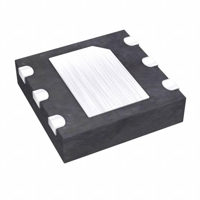
The MAX16815/MAX16828 are available in a
thermally enhanced, 3mm x 3mm, 6-pin TDFN package
with exposed pad and in an 8-pin SO package with
exposed pad; they are specified over the automotive
-40°C to +125°C temperature range.
Applications
●●
●●
●●
●●
●●
Emergency Vehicle Warning Lights
Signage and Indicators
Ambient and Architectural Lighting
LED Bulbs
Display Backlighting
Features
●● 6.5V to 40V Operating Range
●● Adjustable LED Current
MAX16815: 35mA to 100mA
MAX16828: 35mA to 200mA
●● ±3.5% LED Current Accuracy
●● High-Voltage DIM Input for Dimming Interface
●● Integrated Pass Element with Low-Dropout Voltage
(0.4V typ)
●● 5V Regulated Output with 4mA Source Capability
●● Thermal Shutdown
●● Output Short-Circuit Protection
●● Available in Small, Thermally Enhanced,
3mm x 3mm, 6-Pin TDFN and 8-Pin SO with
Exposed Pad Packages
●● -40°C to +125°C Operating Temperature Range
Ordering Information
PART
Pin Configurations appear at end of data sheet.
TEMP RANGE
PIN-PACKAGE
MAX16815ATT+
-40°C to +125°C
6 TDFN-EP*
MAX16815ASA+
-40°C to +125°C
8 SO-EP*
MAX16828ATT+
-40°C to +125°C
6 TDFN-EP*
MAX16828ASA+
-40°C to +125°C
8 SO-EP*
+Denotes a lead(Pb)-free/RoHS-compliant package.
*EP = Exposed pad.
Typical Operating Circuit
+6.5V TO +40V
IN
Simplified Diagram
6.5V TO 40V
OUT
C1
V5
+5V REG
LEDs
IN
C2
EN
MAX16815
MAX16828
GND
CS-
V5
+5V REG
LEDs
0.1µF
CS+
RSENSE
DIM
19-4032; Rev 2; 4/14
MAX16815
MAX16828
CS+
PWM DIMMING
OUT
0.1µF
PWM
DIMMING
RSENSE
DIM
CSGND
�MAX16815/MAX16828
High-Voltage, 100mA/200mA Adjustable Linear
High-Brightness LED Drivers with PWM Dimming
Absolute Maximum Ratings
IN to GND...............................................................-0.3V to +45V
CS+, CS-, V5 to GND..............................................-0.3V to +6V
DIM, EN to GND..........................................-0.3V to (VIN + 0.3V)
OUT Short Circuited to GND Duration
(at VIN = +16V)....................................................... 60 minutes
Maximum Current into Any Pin (except IN and OUT).......±20mA
Continuous Power Dissipation (TA = +70°C)
6-Pin, 3mm x 3mm TDFN
derate 18.2mW/°C above +70°C)............................1454.5mW
8-Pin SO (derate 23.3mW/°C above +70°C)...........1860.5mW
Operating Temperature Range.......................... -40°C to +125°C
Junction Temperature.......................................................+150°C
Junction-to-Case Thermal Resistance (θJC) (Note 1)
6-Pin, 3mm x 3mm TDFN...............................................9°C/W
8-Pin SO.........................................................................7°C/W
Junction-to-Ambient Thermal Resistance (θJA) (Note 1)
6-Pin, 3mm x 3mm TDFN.............................................42°C/W
8-Pin SO.......................................................................43°C/W
Storage Temperature Range............................. -60°C to +150°C
Lead Temperature (soldering, 10s).................................. +300°C
Note 1: Package thermal resistances were obtained using the method described in JEDEC specification JESD51-7, using a four-layer
board. For detailed information on package thermal considerations, refer to www.maximintegrated.com/thermal-tutorial.
Stresses beyond those listed under “Absolute Maximum Ratings” may cause permanent damage to the device. These are stress ratings only, and functional operation of the device at these
or any other conditions beyond those indicated in the operational sections of the specifications is not implied. Exposure to absolute maximum rating conditions for extended periods may affect
device reliability.
Electrical Characteristics
(VIN = 12V, VEN = 12V (SO only), CV5 = 0.1µF to GND, IV5 = 0, VDIM = 4V, VCS- = 0V (SO only), connect RSENSE = 2Ω (MAX16815)
and RSENSE = 1Ω (MAX16828) between CS+ and GND. TA = -40°C to +125°C, unless otherwise noted. Typical values are at
TA = +25°C.) (Note 2)
PARAMETER
Supply Voltage Range
Ground Current
Shutdown Supply Current
Guaranteed Output Current
SYMBOL
VIN
IG
ISHDN
IOUT
Output Current Accuracy
Dropout Voltage
DVDO
Output Current Slew Rate
Short-Circuit Current
CONDITIONS
(Note 3)
MIN
TYP
6.5
MAX
UNITS
40.0
V
ILOAD = 100mA
0.82
2
ILOAD = 200mA
1
2
35
70
VEN ≤ 0.6V (SO only)
RSENSE = 2_ (MAX16815)
100
RSENSE = 1_ (MAX16828)
200
mA
µA
mA
35mA < IOUT < 100mA (MAX16815)
±3.5
35mA < IOUT < 200mA (MAX16828)
±3.5
IOUT = 100mA (current pulsed),
12V < VIN < 40V (MAX16815) (Note 4)
0.1
0.4
IOUT = 100mA (current pulsed),
6.5V < VIN < 12V (MAX16815) (Note 4)
0.1
0.6
IOUT = 200mA (current pulsed),
12V < VIN < 40V (MAX16828) (Note 5)
0.27
0.55
IOUT = 200mA (current pulsed),
6.5V < VIN < 12V (MAX16828) (Note 5)
0.27
0.7
Current rising
9.7
Current falling
9.7
%
V
mA/µs
VOUT = 0V, VIN = 12V, MAX16815
130
200
270
VOUT = 0V, VIN = 12V, MAX16828
250
300
350
-1
-0.2
mA
EN INPUT (SO ONLY)
EN Input Current
IEN
-2.5
EN Input Voltage High
VIH
2.8
EN Input Voltage Low
VIL
www.maximintegrated.com
µA
V
0.6
V
Maxim Integrated │ 2
�MAX16815/MAX16828
High-Voltage, 100mA/200mA Adjustable Linear
High-Brightness LED Drivers with PWM Dimming
Electrical Characteristics (continued)
(VIN = 12V, VEN = 12V (SO only), CV5 = 0.1µF to GND, IV5 = 0, VDIM = 4V, VCS- = 0V (SO only), connect RSENSE = 2Ω (MAX16815)
and RSENSE = 1Ω (MAX16828) between CS+ and GND. TA = -40°C to +125°C, unless otherwise noted. Typical values are at
TA = +25°C.) (Note 2)
PARAMETER
SYMBOL
CONDITIONS
MIN
TYP
MAX
UNITS
VRSNS = VCS+ for TDFN package;
VRSNS = VCS+ - VCS- for SO package
193
200
207
mV
CS- Voltage Range
SO only
-0.3
Input Current (CS+)
VCS+ = 220mV
Input Current (CS-)
VCS+ = 220mV (SO only)
-50
17.2
DIM Input Current
VDIM = 0V
-2.5
-1.0
CURRENT SENSE
Regulated RSENSE Voltage
DIM Input-Voltage High
VRSNS
VIH
2.7
+4.7
V
7
µA
µA
-0.2
2.8
µA
V
DIM Input-Voltage Low
VIL
0.6
V
Turn-On Time
tON
After VDIM rising to 4V (Note 7)
100
µs
Turn-Off Time
tOFF
After VDIM falling to 0.6V (Note 7)
55
µs
THERMAL OVERLOAD
Thermal-Shutdown Temperature
Thermal-Shutdown Hysteresis
+159
°C
24
°C
+5V REGULATOR
Output-Voltage Load Regulation
Output Voltage
V5 Short-Circuit Current
VV5
DVV5
(Note 8)
5.0
5.2
V
0 < IV5 < 4mA
4.8
12
20
mV/mA
VV5 = 0 (Note 9)
15
mA
Note 2: All devices are 100% production tested at TA = +25°C. Limits over the operating temperature range are guaranteed by
design.
Note 3: Resistors were added from OUT to CS+ to aid with power dissipation.
Note 4: Dropout is measured as follows:
Connect RO from OUT to CS+. Connect RSENSE = 2Ω (MAX16815) from CS+ to GND (for TDFN) or from CS+ to CS- (for
SO). Set VIN = 12V (record VOUT1 = VOUT). For VIN = 40V, use RO = 360Ω; for VIN = 6.5V, use RO = 56Ω.
Reduce VIN until VOUT = 0.97 x VOUT1 (record as VIN2 and VOUT2). DVDO = VIN2 - VOUT2.
Note 5: Dropout is measured as follows:
Connect RO from OUT to CS+. Connect RSENSE = 1Ω (MAX16828) from CS+ to GND (for TDFN) or from CS+ to CS- (for
SO). Set VIN = 12V (record VOUT1 = VOUT). For VIN = 40V, use RO = 180Ω; for VIN = 6.5V, use RO = 27Ω.
Reduce VIN until VOUT = 0.97 x VOUT1 (record as VIN2 and VOUT2). ∆VDO = VIN2 - VOUT2.
Note 6: IV5 = 0mA.
Note 7: tON time includes the delay and the rise time needed for IOUT to reach 90% of its final value. tOFF time is the time needed
for IOUT to drop below 10%. See the Typical Operating Characteristics. tON and tOFF are tested with 100Ω (MAX16815) or
51Ω (MAX16828) from OUT to CS+.
Note 8: Current regulation varies with V5 load (see the Typical Operating Characteristics).
Note 9: Thermal shutdown does not function if V5 is shorted to ground.
www.maximintegrated.com
Maxim Integrated │ 3
�MAX16815/MAX16828
High-Voltage, 100mA/200mA Adjustable Linear
High-Brightness LED Drivers with PWM Dimming
Typical Operating Characteristics
(VIN = 12V, TA = +25°C, unless otherwise noted.)
MAX16815 ILOAD = 100mA
MAX16815 AND MAX16828 ILOAD = 35mA
50
-40 -25 -10 5 20 35 50 65 80 95 110 125
5V REGULATOR OUTPUT (V)
0
-40 -25 -10 5 20 35 50 65 80 95 110 125
MAX16815 toc03
5
10
15
20
25
30
35
40
MAX16815 AND MAX16828
5.1
5.0
4.9
4.8
NO LOAD
IV5 = 1mA
IV5 = 5mA
-40 -25 -10 5 20 35 50 65 80 95 110 125
0.4
MAX16815 toc06
5.2
MAX16815 AND MAX16828
0.3
0.2
0.1
0
0
1
2
3
4
TEMPERATURE (C)
TEMPERATURE (C)
IV5 (mA)
+5V REGULATOR OUTPUT vs. VIN
MAX16815 200Hz DIMMED OPERATION
MAX16815 200Hz DIMMED OPERATION
(EXPANDED)
MAX16815 AND MAX16828
5.0
4.9
MAX16815 toc08
ILOAD = 100mA, VIN = 12V
DIM PULSED AT 200Hz
150% DUTY CYCLE
NO LOAD
IV5 = 1mA
IV5 = 5mA
5
0
35 40 45 50 55 60 65 70 75 80 85 90 95 100
VCS+ (FOR TDFN) OR VCS+ - VCS- (FOR SO)
vs. IV5
5.1
4.8
100
50
MAX16815 ILOAD = 100mA
5.2
MAX16815
150
+5V REGULATOR OUTPUT
vs. TEMPERATURE
0.2
0
200
DROPOUT VOLTAGE
vs. TEMPERATURE
0.3
0.1
MAX16828
250
INPUT VOLTAGE (V)
MAX16828 ILOAD = 200mA
0.4
300
OUTPUT CURRENT (mA)
MAX16815 toc07
DROPOUT VOLTAGE (V)
0.5
0.1
350
TEMPERATURE (C)
MAX16815 toc04
0
0.2
OUTPUT CURRENT
vs. INPUT VOLTAGE
400
VCS+ (FOR TDFN) OR VCS+ - VCS- (FOR SO) (V)
100
0.3
MAX16815 toc05
150
MAX16815 AND MAX16828
IOUT UP TO 100mA FOR MAX16828
OUTPUT CURRENT (mA)
200
0.4
VCS+ (FOR TDFN) OR VCS+ - VCS- (FOR SO)
vs. OUTPUT CURRENT
MAX16815 toc02
MAX16828 ILOAD = 200mA
5V REGULATOR OUTPUT (V)
OUTPUT CURRENT (mA)
250
MAX16815 toc01
300
VCS+ (FOR TDFN) OR VCS+ - VCS- (FOR SO) (V)
OUTPUT CURRENT
vs. TEMPERATURE
10
15
20
25
30
35
40
1ms/div
MAX16815 toc09
VDIM
10V/div
ILOAD = 100mA, VIN = 12V
DIM PULSED AT 200Hz
150% DUTY CYCLE
VDIM
10V/div
0V
0V
ILOAD
50mA/div
ILOAD
50mA/div
0
0
10s/div
VIN (V)
www.maximintegrated.com
Maxim Integrated │ 4
�MAX16815/MAX16828
High-Voltage, 100mA/200mA Adjustable Linear
High-Brightness LED Drivers with PWM Dimming
Typical Operating Characteristics (continued)
(VIN = 12V, TA = +25°C, unless otherwise noted.)
MAX16815 200Hz DIMMED OPERATION
(EXPANDED)
MAX16828 200Hz DIMMED OPERATION
MAX16815 toc10
ILOAD = 100mA, VIN = 12V
DIM PULSED AT 200Hz
50% DUTY CYCLE
MAX16815 toc11
VDIM
10V/div
ILOAD = 200mA, VIN = 12V
DIM PULSED AT 200Hz
50% DUTY CYCLE
VDIM
10V/div
0V
0V
ILOAD
50mA/div
ILOAD
200mA/div
0
0
20s/div
1ms/div
MAX16828 200Hz DIMMED OPERATION
(EXPANDED)
MAX16828 200Hz DIMMED OPERATION
(EXPANDED)
MAX16815 toc12
ILOAD = 200mA, VIN = 12V
DIM PULSED AT 200Hz
50% DUTY CYCLE
20s/div
www.maximintegrated.com
MAX16815 toc13
VDIM
10V/div
ILOAD = 200mA, VIN = 12V
DIM PULSED AT 200Hz
50% DUTY CYCLE
VDIM
10V/div
0V
0V
ILOAD
200mA/div
0
ILOAD
200mA/div
0
20s/div
Maxim Integrated │ 5
�MAX16815/MAX16828
High-Voltage, 100mA/200mA Adjustable Linear
High-Brightness LED Drivers with PWM Dimming
Pin Description
TDFN
PIN
SO
NAME
FUNCTION
1
6
DIM
Pulsed Dimming Input. Drive DIM low to turn off output current (LED current). Drive DIM
high to turn on the output current (LED current). DIM is pulled high to VIN when left
unconnected
—
7
EN
Enable Input. Drive EN high to enable the output. For the TDFN package, this input is not
accessible and always high
2
8
OUT
3
1
IN
4
2
CS+
LED Current-Sense Amplifier Positive Input. For the SO package version, connect the
current-sense resistor between this pin and CS-; for the TDFN version, connect it between
this pin and ground.
—
3
CS-
LED Current-Sense Amplifier Negative Input. Connect to ground
5
4
V5
+5V Regulated Output. Connect a 0.1µF (min) capacitor from V5 to GND
6
5
GND
—
—
EP
Current-Regulated Output
Positive Input Supply. Bypass IN with a 0.1µF (min) capacitor to GND
Ground
Exposed Pad. Connect to a large ground plane for effective power dissipation. Do not use as
the only ground connection.
DFN Functional Diagram
DIM
IN
0.8A
V5
BANDGAP
AND 5V
REGULATOR
1.2V
IREG
P
OUT
THERMAL
SHUTDOWN
CS+
DIFF
AMP
GND
MAX16815
MAX16828
www.maximintegrated.com
Maxim Integrated │ 6
�MAX16815/MAX16828
High-Voltage, 100mA/200mA Adjustable Linear
High-Brightness LED Drivers with PWM Dimming
SO Functional Diagram
DIM
IN
0.8A
EN
V5
BANDGAP
AND 5V
REGULATOR
1.2V
IREG
P
OUT
THERMAL
SHUTDOWN
CS+
DIFF
AMP
GND
MAX16815
MAX16828
CS-
Detailed Description
Applications Information
+5V Regulator
Programming the LED Current
The MAX16815/MAX16828 include a fixed +5V output
regulator that delivers up to 4mA of load current throughout the 6.5V to 40V input voltage range. Connect a 0.1µF
compensation capacitor from V5 to ground. Shorting V5
to ground disables the thermal shutdown. V5 stays on
during PWM dimming.
Thermal Protection
The MAX16815/MAX16828 enter a thermal-shutdown
mode in the event of overheating. This typically occurs
in overload or output short-circuit conditions. If the
junction temperature exceeds TJ = +159°C (typ), the
internal thermal-protection circuitry turns off the series
pass device. The MAX16815/MAX16828 recover from
thermal-shutdown mode once the junction temperature drops by 24°C (typ). The devices therefore protect
themselves by thermal cycling in the event of a shortcircuit or overload condition. Shorting V5 to ground
disables the thermal shutdown.
www.maximintegrated.com
The MAX16815/MAX16828 use a sense resistor across
CS+ and GND for the TDFN package or across CS+ and
CS- for the SO package, to set the LED current. The LED
current is given by ILED = VRSNS/RSENSE.
Input-Voltage Considerations
For proper operation, the minimum input voltage must
always be:
VIN(MIN) ≥ VRSNS(MAX) + VFT(MAX) + ∆VDO(MAX)
where VFT(MAX) is the total forward voltage of all series
connected LEDs. The minimum operating voltage of
the device is +6.5V. The device operates below +6.5V;
however, output current may not meet the full regulation
specification (see the Typical Operating Characteristics)
and the V5 regulator will drop below 5V.
Low-Frequency PWM Dimming
at the Output
Provide a pulse to the dimming input (DIM) of the
MAX16815/MAX16828 to produce a PWM output.
Alternatively, connect DIM to IN and pulse IN.
Maxim Integrated │ 7
�MAX16815/MAX16828
High-Voltage, 100mA/200mA Adjustable Linear
High-Brightness LED Drivers with PWM Dimming
D1
STOP
D2
TAIL
IN
OUT
R1
MAX16815
MAX16828
R2
D3
IN
DIS
OUT
R3
C1
D4
ICM7555
TH
TRG
R4*
V5
+5V REG
LEDs
C2
DIM
CS+
GND
RSENSE
GND
CS-
C2
*R4 < 300k
Figure 1. PWM Dimming Operation with ICM7555 Timer
Two Brightness Levels for
TAIL/STOP Lights
Figure 1 shows PWM dimming operation for the
MAX16815/MAX16828 with an ICM7555 timer. The
ICM7555 provides adjustable duty cycle using two external resistors and a capacitor. In TAIL operation, the output
of the ICM7555 feeds into DIM and lights up the LEDs.
The LED’s brightness depends on the duty cycle of the
ICM7555. When VSTOP is present, DIM is pulled up to
VSTOP. The PWM dimming operation is disabled and the
LEDs light up to full brightness. See the ICM7555 data
sheet for formulas to calculate the dimming frequency and
the duty cycle.
VIN
C1
IN
OUT
MAX16815
MAX16828
PWM
DIMMING
LEDs
V5
C2
DIM
CS+
RT
R2
GND
R1
CS-
LED Current Thermal Foldback
With a minimum number of external components, the
MAX16815/MAX16828 provide LED current thermal foldback using a negative temperature coefficient (NTC)
thermistor. Figure 2 shows a thermistor connected to V5
and the CS+ of the MAX16815/MAX16828. As the temperature increases, the voltage drop across R2 increases,
causing the LED current to decrease.
ILED = [VRSNS - (R2 / RT) (VV5 - VRSNS)]/R1
Other Applications
The application circuit in Figure 3 implements a twolevel brightness current for TAIL/STOP lights. In TAIL
operation, Q1 is off and R1 sets the output current. In
www.maximintegrated.com
Figure 2. LED Current Thermal Foldback with an NTC
Thermistor
STOP operation, Q1 turns on and the output current
is set by a parallel combination of R1 and R2. Figure
4 shows an application circuit with the MAX16815/
MAX16828 using a single BJT to provide high output
current. For proper operation:
VIN(MIN) > VCESAT(MAX) + VFT(MAX) + VRSNS
where VCESAT(MAX) is the maximum saturation voltage
of the external BJT and VFT(MAX) is the total forward
voltage of all series connected LEDs.
Maxim Integrated │ 8
�MAX16815/MAX16828
High-Voltage, 100mA/200mA Adjustable Linear
High-Brightness LED Drivers with PWM Dimming
STOP
LEDs
D1
OUT
IN
TAIL
DIM
MAX16815
MAX16828
C1
VIN
V5
C2
LEDs
IN
R3
MAX16815
MAX16828
C1
CS+
PWM
DIMMING
R2
GND
Q1
CS+
GND
RSENSE
Z1
CS-
CS-
Figure 3. Two-Level Brightness with Current Level Switch for
TAIL/STOP Lights
Figure 4. Increased LED Current (Ampere Range)
with a Single BJT
D1
L1
VIN
V5
C2
DIM
R1
Q1
OUT
CREF
C2
REF
VCC
C3
IN
R3
MAX5094C
CCOMP
COMP
RCOMP
OUT
Q1
EN
C4
LEDs
C7
DIM
GND
EN
V5
C6
FB
IN
OUT
U2
MAX16815
MAX16828
LEDs
C11
DIM
CT/RT
R4
CS
GND
CS-
OUT
U3
MAX16815
MAX16828
LEDs
V5
C9
C8
DIM
CS+
R5
CT
EN
V5
C10
CS+
IN
OUT
U4
MAX16815
MAX16828
CS+
R7
GND
CS-
R6
GND
CS-
R2
Figure 5. Multichannel HB LED Drivers for LCD Backlight
Multichannel HB LED Driver
Figure 5 shows an array of MAX16815/MAX16828s with
independent DIM control. The MAX5094C, a currentmode PWM controller, provides the input power to each
LED driver preregulated voltage to multiple MAX16815/
MAX16828 drivers.
www.maximintegrated.com
Chip Information
PROCESS: BiCMOS
Maxim Integrated │ 9
�MAX16815/MAX16828
High-Voltage, 100mA/200mA Adjustable Linear
High-Brightness LED Drivers with PWM Dimming
Pin Configurations
GND
V5
CS+
TOP VIEW
6
5
4
MAX16815
MAX16828
8
OUT
2
7
EN
CS-
3
6
DIM
5
GND
MAX16815
MAX16828
EP*
SO
2
3
OUT
IN
DIM
1
1
V5 4
EP*
+
IN
CS+
TDFN
*EP = EXPOSED PAD
Package Information
For the latest package outline information and land patterns (footprints), go to www.maximintegrated.com/packages. Note that a “+”,
“#”, or “-” in the package code indicates RoHS status only. Package drawings may show a different suffix character, but the drawing
pertains to the package regardless of RoHS status.
PACKAGE TYPE
8 SO-EP
6 TDFN-EP
www.maximintegrated.com
PACKAGE CODE
S8E-12
T633-2
DOCUMENT NO.
21-0111
21-0137
Maxim Integrated │ 10
�MAX16815/MAX16828
High-Voltage, 100mA/200mA Adjustable Linear
High-Brightness LED Drivers with PWM Dimming
Revision History
REVISION
NUMBER
REVISION
DATE
PAGES
CHANGED
0
2/08
Initial release
1
7/09
Added the SO package to the Ordering Information table, Electrical Characteristics,
TOC 2 and TOC 6, Pin Description table, and Functional Diagrams; modified the
Simplified Diagram and Figures 1–4 to include the CS- pin; and added the SO-EP
Pin Configuration
2
4/14
No /V OPNs; removed automotive references from Applications section
DESCRIPTION
—
1–4, 6–10
1
For pricing, delivery, and ordering information, please contact Maxim Direct at 1-888-629-4642, or visit Maxim Integrated’s website at www.maximintegrated.com.
Maxim Integrated cannot assume responsibility for use of any circuitry other than circuitry entirely embodied in a Maxim Integrated product. No circuit patent licenses
are implied. Maxim Integrated reserves the right to change the circuitry and specifications without notice at any time. The parametric values (min and max limits)
shown in the Electrical Characteristics table are guaranteed. Other parametric values quoted in this data sheet are provided for guidance.
Maxim Integrated and the Maxim Integrated logo are trademarks of Maxim Integrated Products, Inc.
© 2014 Maxim Integrated Products, Inc. │ 11
�