0
登录后你可以
  • 下载海量资料
  • 学习在线课程
  • 观看技术视频
  • 写文章/发帖/加入社区
会员中心
创作中心
发布
  • 发文章

  • 发资料

  • 发帖

  • 提问

  • 发视频

创作活动
MAX186AEAP+

MAX186AEAP+

  • 厂商:

    AD(亚德诺)

  • 封装:

    SSOP-20

  • 描述:

    数据采集系统(DAS),ADC 12 b 133k MICROWIRE™,QSPI™,串行,SPI™ 20-SSOP

  • 详情介绍
  • 数据手册
  • 价格&库存
MAX186AEAP+ 数据手册
EVALUATION KIT AVAILABLE MAX186/MAX188 Low-Power, 8-Channel, Serial 12-Bit ADCs General Description The MAX186/MAX188 are 12-bit data-acquisition systems that combine an 8-channel multiplexer, highbandwidth track/hold, and serial interface together with high conversion speed and ultra-low power consumption. The devices operate with a single +5V supply or dual ±5V supplies. The analog inputs are software configurable for unipolar/bipolar and single-ended/differential operation. The 4-wire serial interface directly connects to SPI, QSPI™ and MICROWIRE® devices without external logic. A serial strobe output allows direct connection to TMS320 family digital signal processors. The MAX186/MAX188 use either the internal clock or an external serial-interface clock to perform successiveapproximation A/D conversions. The serial interface can operate beyond 4MHz when the internal clock is used. ____________________________Features o 8-Channel Single-Ended or 4-Channel Differential Inputs o Single +5V or ±5V Operation o Low Power: 1.5mA (Operating Mode) 2µA (Power-Down Mode) o Internal Track/Hold, 133kHz Sampling Rate o Internal 4.096V Reference (MAX186) o SPI-/QSPI-/MICROWIRE-/TMS320-Compatible 4-Wire Serial Interface o Software-Configurable Unipolar or Bipolar Inputs o 20-Pin PDIP, SO, SSOP Packages o Evaluation Kit Available Ordering Information † PART TEMP RANGE PIN-PACKAGE The MAX186 has an internal 4.096V reference while the MAX188 requires an external reference. Both parts have a reference-buffer amplifier that simplifies gain trim . MAX186_CPP+ 0°C to +70°C 20 PDIP MAX186_CWP+ 0°C to +70°C 20 SO MAX186_CAP+ 0°C to +70°C 20 SSOP The MAX186/MAX188 provide a hard-wired SHDN pin and two software-selectable power-down modes. Accessing the serial interface automatically powers up the devices, and the quick turn-on time allows the MAX186/MAX188 to be shut down between every conversion. Using this technique of powering down between conversions, supply current can be cut to under 10µA at reduced sampling rates. MAX186DC/D 0°C to +70°C Dice* MAX186_EPP+ -40°C to +85°C 20 PDIP MAX186_EWP+ -40°C to +85°C 20 SO MAX186_EAP+ -40°C to +85°C 20 SSOP The MAX186/MAX188 are available in 20-pin PDIP and SO packages, and in a shrink small-outline package (SSOP), that occupies 30% less area than an 8-pin PDIP. For applications that call for a parallel interface, see the MAX180/MAX181 data sheet. For anti-aliasing filters, consult the MAX274/MAX275 data sheet. ________________________Applications Portable Data Logging Data-Acquisition High-Accuracy Process Control Automatic Testing Robotics Battery-Powered Instruments Medical Instruments QSPI is a trademark of Motorola. MICROWIRE is a registered trademark of National Semiconductor. Ordering Information continued on last page. †Parts are offered in grades A, B, C and D (grades defined in Electrical Characteristics). When ordering, please specify grade. Contact factory for availability of A-grade in SSOP package. *Dice are specified at +25°C, DC parameters only. +Denotes a lead(Pb)-free/RoHS-compliant package. ____________________Pin Configuration TOP VIEW + CH0 1 20 VDD CH1 2 19 SCLK CH2 3 18 CS CH3 4 CH4 5 MAX186 MAX188 17 DIN 16 SSTRB CH5 6 15 DOUT CH6 7 14 DGND CH7 8 13 AGND VSS 9 12 REFADJ 11 VREF SHDN 10 PDIP/SO/SSOP For pricing, delivery, and ordering information, please contact Maxim Direct at 1-888-629-4642, or visit Maxim Integrated’s website at www.maximintegrated.com. 19-0123; Rev 5; 1/12 MAX186/MAX188 Low-Power, 8-Channel, Serial 12-Bit ADCs ABSOLUTE MAXIMUM RATINGS VDD to AGND............................................................-0.3V to +6V VSS to AGND ............................................................+0.3V to -6V VDD to VSS ..............................................................-0.3V to +12V AGND to DGND.....................................................-0.3V to +0.3V CH0–CH7 to AGND, DGND .............(VSS - 0.3V) to (VDD + 0.3V) CH0–CH7 Total Input Current...........................................±20mA VREF to AGND ...........................................-0.3V to (VDD + 0.3V) REFADJ to AGND.......................................-0.3V to (VDD + 0.3V) Digital Inputs to DGND...............................-0.3V to (VDD + 0.3V) Digital Outputs to DGND ............................-0.3V to (VDD + 0.3V) Digital Output Sink Current .................................................25mA Continuous Power Dissipation (TA = +70°C) PDIP (derate 11.11mW/°C above +70°C) .....................889mW SO (derate 10.00mW/°C above +70°C) ........................800mW SSOP (derate 8.00mW/°C above +70°C) .....................640mW Operating Temperature Ranges MAX186_C/MAX188_C ........................................0°C to +70°C MAX186_E/MAX188_E......................................-40°C to +85°C Storage Temperature Range .............................-60°C to +150°C Lead Temperature (soldering, 10s) .................................+300°C Soldering Temperature (reflow) .......................................+260°C Stresses beyond those listed under “Absolute Maximum Ratings” may cause permanent damage to the device. These are stress ratings only, and functional operation of the device at these or any other conditions beyond those indicated in the operational sections of the specifications is not implied. Exposure to absolute maximum rating conditions for extended periods may affect device reliability. ELECTRICAL CHARACTERISTICS (VDD = 5V ±5%; VSS = 0V or -5V; fCLK = 2.0MHz, external clock (50% duty cycle); 15 clocks/conversion cycle (133ksps); MAX186— 4.7µF capacitor at VREF pin; MAX188—external reference, VREF = 4.096V applied to VREF pin; TA = TMIN to TMAX, unless otherwise noted.) PARAMETER SYMBOL CONDITIONS MIN TYP MAX UNITS DC ACCURACY (Note 1) Resolution 12 Relative Accuracy (Note 2) Differential Nonlinearity DNL Offset Error Bits MAX186A/MAX188A ±0.5 MAX186B/MAX188B ±0.5 MAX186C ±1.0 MAX188C ±0.75 MAX186D/MAX188D ±1.0 No missing codes over temperature ±1 MAX186A/MAX188A ±2.0 MAX186B/MAX188B ±3.0 MAX186C/MAX188C ±3.0 MAX186D/MAX188D ±3.0 MAX186 (all grades) Gain Error (Note 3) External reference 4.096V (MAX188) Gain Temperature Coefficient LSB LSB LSB ±3.0 MAX188A ±1.5 MAX188B ±2.0 MAX188C ±2.0 MAX188D ±3.0 External reference, 4.096V Channel-to-Channel Offset Matching LSB ±0.8 ppm/°C ±0.1 LSB DYNAMIC SPECIFICATIONS (10kHz sine wave input, 4.096VP-P, 133ksps, 2.0MHz external clock, bipolar input mode) Signal-to-Noise + Distortion Ratio Total Harmonic Distortion (up to the 5th harmonic) THD Spurious-Free Dynamic Range SFDR Channel-to-Channel Crosstalk 2 SINAD 70 dB -80 80 65kHz, VIN = 4.096VP-P (Note 4) dB dB -85 dB Maxim Integrated MAX186/MAX188 Low-Power, 8-Channel, Serial 12-Bit ADCs ELECTRICAL CHARACTERISTICS (continued) (VDD = 5V ±5%; VSS = 0V or -5V; fCLK = 2.0MHz, external clock (50% duty cycle); 15 clocks/conversion cycle (133ksps); MAX186— 4.7µF capacitor at VREF pin; MAX188—external reference, VREF = 4.096V applied to VREF pin; TA = TMIN to TMAX, unless otherwise noted.) PARAMETER SYMBOL Small-Signal Bandwidth CONDITIONS MIN -3dB rolloff Full-Power Bandwidth TYP MAX UNITS 4.5 MHz 800 kHz CONVERSION RATE Conversion Time (Note 5) Track/Hold Acquisition Time t CONV Internal clock External clock, 2MHz, 12 clocks/conversion 5.5 10 6 tAZ 1.5 µs µs Aperture Delay 10 ns Aperture Jitter
MAX186AEAP+
物料型号:MAX186/MAX188 器件简介:MAX186/MAX188是12位数据采集系统,集成了8通道多路复用器、高带宽跟踪/保持器和串行接口,具有高速转换和超低功耗的特点。

支持单+5V或双±5V供电,模拟输入可软件配置为单极性/双极性和单端/差分操作。

提供SPI、QSPI、MICROWIRE和TMS320兼容的4线串行接口。

引脚分配:1-8为CH0-CH7模拟输入引脚,9为VSS负电源,10为SHDN三态关闭输入,11为VREF参考电压输出,12为REFADJ参考缓冲放大器输入,13为AGND模拟地,14为DGND数字地,15为DOUT串行数据输出,16为SSTRB串行输出时钟,17为DIN串行数据输入,18为CS片选,19为SCLK串行时钟,20为VDD正电源。

参数特性:12位分辨率,1.5mA(操作模式)和2µA(电源关闭模式)的低功耗,133kHz的采样率,内部4.096V参考电压(MAX186)或外部参考电压(MAX188),软件可配置的单极性或双极性输入。

功能详解:器件使用逐次逼近的模数转换技术,无需外部保持电容。

提供硬件关闭引脚和两种软件可选的电源关闭模式。

器件在每次转换之间自动关闭,以降低功耗。

应用信息:便携式数据记录、数据采集、高精度过程控制、自动测试、机器人技术、电池供电仪器、医疗仪器。

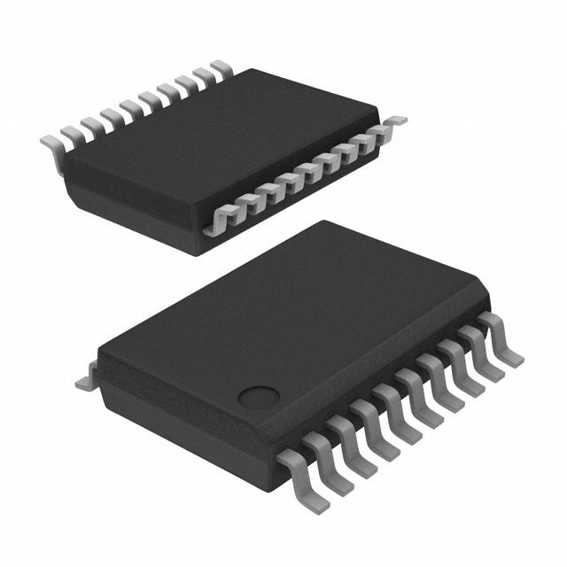
封装信息:提供20引脚PDIP、SO和SSOP封装。

MAX186还提供Dice封装。

所有封装均符合RoHS标准。


以上摘要信息为MAX186/MAX188数据手册的主要内容,包括技术规格、功能描述、应用领域和封装选项等。
MAX186AEAP+ 价格&库存

很抱歉,暂时无法提供与“MAX186AEAP+”相匹配的价格&库存,您可以联系我们找货

免费人工找货
MAX186AEAP+
  •  国内价格
  • 1+339.53040
  • 200+131.39280
  • 500+126.78120
  • 1000+124.50240

库存:0

MAX186AEAP+
  •  国内价格 香港价格
  • 1+682.587251+84.57674
  • 10+566.1686810+70.15176
  • 66+513.4585266+63.62065
  • 132+500.12123132+61.96808

库存:80