物料型号:
- MAX196ACNI
- MAX196BCNI
- MAX196ACWI
- MAX196BCWI
- MAX196ACAI
- MAX196BCAI
器件简介:
MAX196/MAX198是12位数据采集系统(DAS),仅需单一+5V供电,能够将高达±10V(MAX196)和±4V(MAX198)的模拟信号转换为数字信号。这些系统提供6个模拟输入通道,可通过软件独立编程以适应不同的范围。
引脚分配:
- CLK:时钟输入
- CS:芯片选择,低电平有效
- D11-D0:三态数字输出,D11为最高位
- AGND:模拟地
- CH5-CH0:模拟输入通道
- REFADJ:带隙电压参考输出,外部调整引脚
- REF:参考缓冲器输出/ADC参考输入
- INT:中断信号,转换完成时低电平
- RD:读操作使能
- WR:写操作使能
- VDD:+5V供电
- DGND:数字地
参数特性:
- 分辨率:12位
- 积分非线性:±1/2 LSB(MAX196A/MAX198A)或±1 LSB(MAX196B/MAX198B)
- 微分非线性:±1 LSB
- 偏移误差:+3 LSB(MAX196A/MAX198A)或±10 LSB(MAX196B/MAX198B)
- 增益误差:+7 LSB(MAX196A/MAX198A)或±10 LSB(MAX196B/MAX198B)
- 信噪比加失真比:MAX196A/MAX198A为70dB,MAX196B/MAX198B为69dB
- 总谐波失真:高达-85dB至-78dB
- 无杂散动态范围:80dB
功能详解:
- 这些转换器使用连续逼近和内部输入跟踪/保持(T/H)电路将模拟信号转换为12位数字输出。
- 提供内部或外部时钟模式。
- 两个可编程的电源关闭模式(STBYPD, FULLPD)在转换之间提供低电流关闭。
- 内部或外部采集控制。
- 12位并行接口。
应用信息:
- 工业控制系统
- 机器人
- 数据采集系统
- 自动测试系统
- 医疗仪器
- 电信
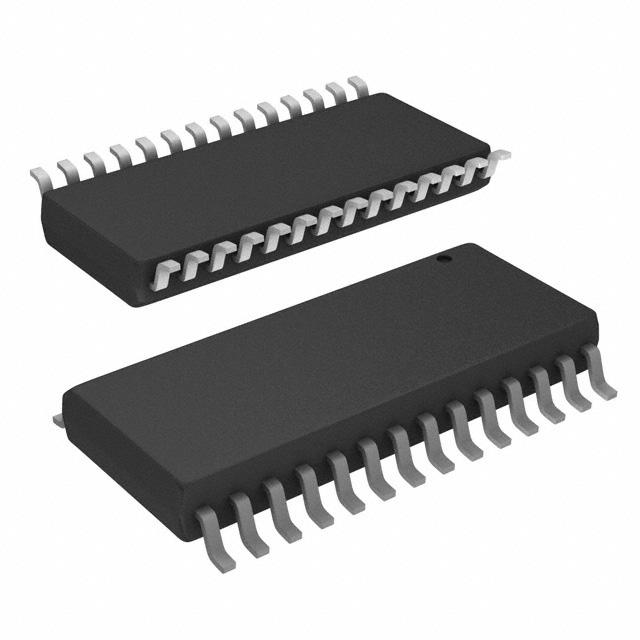
封装信息:
- 28引脚窄塑料DIP
- 28引脚宽SO
- 28引脚SSOP
- 陶瓷SB封装