Click here for production status of specific part numbers.
MAX25256
Automotive, 36V H-Bridge Transformer Driver
for Isolated Supplies
General Description
Benefits and Features
The MAX25256 H-bridge transformer driver provides
a simple solution for making isolated power supplies
up to 10W. The device drives a transformer’s primary
coil with up to 300mA of current from a wide 8V to 36V
direct current (DC) supply. The transformer’s
secondary-to-primary winding ratio defines the output
voltage, allowing selection of virtually any isolated
output voltage.
•
Simple, Flexible Design
• 8V to 36V Supply Range
• Up to 90% Efficiency
• Provides Up to 10W to the Transformer
• Undervoltage Lockout (UVLO)
• 2.5V to 5V Compatible Logic Interface
• Internal or External Clock Source
• Adjustable Overcurrent Threshold
The device features adjustable current limiting,
allowing indirect limiting of secondary-side load
currents. The current limit of the MAX25256 is set by
an external resistor. A
output asserts when
the device detects an overtemperature or overcurrent
condition. In addition, the device features a low-power
mode to reduce the overall supply current to 0.65mA
(typ) when the driver is not in use.
•
Integrated System Protection
• Fault Detection and Indication
• Overcurrent Limiting
• Overtemperature Protection
•
Saves Space on Board
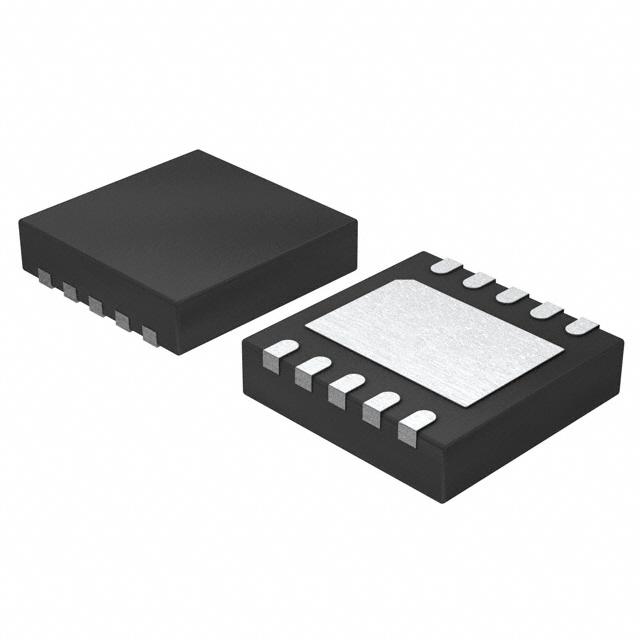
• Small 10-Pin TDFN Package (3mm x 3mm)
• AECQ-100 Qualified
The device can be operated using the internal
oscillator or driven by an external clock to synchronize
multiple MAX25256 devices and precisely set the
switching frequency. Internal circuitry guarantees a
fixed 50% duty cycle to prevent DC flow through the
transformer, regardless of which clock source is used.
The device is available in a small 10-pin (3mm x
3mm) TDFN package and is specified over the -40°C
to +125°C automotive temperature range.
Applications
•
•
•
•
Isolated Gate Driver Supplies
Isolated Supplies for Motor Control
Dual-Battery Systems
Isolated Supplies for controller area network (CAN),
serial peripheral interface (SPI), I2C, etc.
19-101087; Rev 0; 4/21
�MAX25256
Automotive, 36V H-Bridge Transformer Driver for
Isolated Supplies
Simplified Block Diagram
VIN
CIN
1µF
VDD
4.6k
VOUT
n:1
FAULT
ST1
EN
CLK
COUT
2-4µF
MAX25256
ST2
ITH
RLIM
GND
Absolute Maximum Ratings
VDD,
...................................................... -0.3V to +40V
Operating Temperature Range ...................... -40°C to +125°C
ST1, ST2 ............................................... -0.3V to (VDD + 0.3V)
Operating Junction Temperature (Note 1) .................... +150°C
CLK, ITH,
Storage Temperature Range ......................... -65°C to +150°C
........................................................ -0.3V to +6V
Continuous Current .......................................... ±50mA
ST1, ST2 Continuous Current .................................... ±850mA
Lead Temperature (soldering, 10s) .............................. +300°C
Soldering Temperature (reflow).................................... +260°C
TDFN (Single-Layer Board) (Derate 18.5mW/°C above +70°C)
............................................................................... 1481.5mW
Stresses beyond those listed under “Absolute Maximum Ratings” may cause permanent damage to the device. These are stress ratings only, and functional operation of the device at these or
any other conditions beyond those indicated in the operational sections of the specifications is not implied. Exposure to absolute maximum rating conditions for extended periods may affect
device reliability.
Package Information
10 TDFN-EP
Package Code
T1033+1C
Outline Number
21-0137
Land Pattern Number
90-0003
Thermal Resistance, Single-Layer Board:
www.maximintegrated.com
Maxim Integrated | 2
�MAX25256
Automotive, 36V H-Bridge Transformer Driver for
Isolated Supplies
Junction-to-Ambient (θJA)
54°C/W
Junction-to-Case Thermal Resistance (θJC)
9°C/W
Thermal Resistance, Four-Layer Board:
Junction-to-Ambient (θJA)
41°C/W
Junction-to-Case Thermal Resistance (θJC)
9°C/W
For the latest package outline information and land patterns (footprints), go to www.maximintegrated.com/packages. Note that a “+”, “#”, or “-” in the
package code indicates RoHS status only. Package drawings may show a different suffix character, but the drawing pertains to the package regardless
of RoHS status.
Package thermal resistances were obtained using the method described in JEDEC specification JESD51-7, using a four-layer board. For detailed
information on package thermal considerations, refer to www.maximintegrated.com/thermal-tutorial.
Electrical Characteristics
(VDD = 8V to 36V, V
= 0V, TA = -40°C to +125°C unless otherwise noted, Typical values are at TA = +25°C (Note 2))
PARAMETER
SYMBOL
CONDITIONS
MIN
TYP
MAX
UNITS
DC CHARACTERISTICS
Supply Voltage
Range
VDD
(Note 3)
Supply Current
IDD
V = 0.8V, VCLK = 0V, RLIM = 1000Ω,
ST1/ST2 not connected
6
11
Disable Supply
Current
IDIS
V = 3.3V, VCLK = 0V
0.7
1.1
ROH
ST1 = ST2 = high, IST1, ST2 = +300mA,
RLIM = 1000Ω
1
1.8
ROL
ST1 = ST2 = low, IST1, ST2 = -300mA,
RLIM = 1000Ω
0.6
1.0
6.3
6.9
Driver Output
Resistance
UndervoltageLockout Threshold
VUVLO
UndervoltageLockout Threshold
Hysteresis
VUVLO_HYST
VDD rising
ILIM
ST1, ST2 Leakage
Current
LOGIC SIGNALS (CLK,
ILKG
RLIM = 3010Ω, VDD = 24V
V = 3.3V, VCLK = 0V,
VST1 = VST2 = 0V or VDD, TA = +25°C
V
mA
mA
Ω
5.9
500
650
V
mV
800
mA
165
-1
215
265
+1
µA
)
Input Logic-High
Voltage
VIH
Input Logic-Low
Voltage
VIL
www.maximintegrated.com
36
300
RLIM = 1000Ω, VDD = 24V
ST1, ST2 Current
Limit
8
2
V
0.8
V
Maxim Integrated | 3
�MAX25256
(VDD = 8V to 36V, V
Automotive, 36V H-Bridge Transformer Driver for
Isolated Supplies
= 0V, TA = -40°C to +125°C unless otherwise noted, Typical values are at TA = +25°C (Note 2))
PARAMETER
Input Leakage
Current
Output LogicLow Voltage
SYMBOL
IIL
CONDITIONS
VCLK = V
= 5.5V or 0V
MIN
TYP
-1
MAX
UNITS
+1
µA
1
V
10
µA
VOL
I
= 10mA
ILKGF
V
= 36V,
Switching Frequency
fSW
VCLK = 0V, measured at ST1/ST2
outputs
255
700
kHz
CLK Input Frequency
fEXT
External clocking
200
2000
kHz
Internal or external clocking,
Fext1000kHz
(Note 4)
48
49
50
Leakage
Current
deasserted
AC CHARACTERISTICS
ST1/ST2 Duty Cycle
DTC
%
ST1/ST2 Rise Time
tRISE
ST1/ ST2 = 20% to 80% of VDD, RL =
1kΩ,
CL = 50pF, Figure 1A
100
ST1/ST2 Fall Time
tFALL
ST1/ST2 = 80% to 20% of VDD, RL =
1kΩ,
CL = 50pF, Figure 1A
100
Crossover Dead Time
tDEAD
Watchdog Timeout
tWDOG
(Note 5), VDD = 36V
20
32
55
Current-Limit
Blanking Time
tBLANK
Figure 2, VDD = 36V
0.73
1.2
2.0
Current-Limit
Autoretry Time
tRETRY
Figure 2, VDD = 36V
23.4
38.4
64.0
RL = 200Ω, Figure 1B
ns
ns
ns
30
µs
ms
ms
PROTECTION
Thermal-Shutdown
Threshold
TSHDN
Thermal-Shutdown
Hysteresis
TSHDN_HYS
+160
°C
10
°C
Note 1: Limits are 100% tested at TA = +25°C. Limits over the operating temperature range and relevant supply voltage are
guaranteed by design and characterization. Typical values are at T A = +25°C.
Note 2: If VDD is greater than 27V, see the Snubber section.
Note 3: Guaranteed by design and simulation; not production tested.
Note 4: See the Watchdog section.
www.maximintegrated.com
Maxim Integrated | 4
�MAX25256
Automotive, 36V H-Bridge Transformer Driver for
Isolated Supplies
Test Circuits/Timing Diagrams
ST1/ST2
ST1
CL
RL
RL
ST2
(B)
(A)
VDD
80%
80%
ST1
0V
20%
20%
tDEAD
VDD
tRISE
tFALL
ST2
0V
(C)
Figure 1. Test Circuits (A and B) and Timing Diagram (C) for Rise, Fall, and Dead Times
ILIM
IST1,ST2
50%
tBLANK
50%
tRETRY
50%
0mA
Figure 2. Timing Diagram for Current Limiting
www.maximintegrated.com
Maxim Integrated | 5
�MAX25256
Automotive, 36V H-Bridge Transformer Driver for
Isolated Supplies
Typical Operating Characteristics
VDD = 24V, TA = +25oC, unless otherwise stated
www.maximintegrated.com
Maxim Integrated | 6
�MAX25256
Automotive, 36V H-Bridge Transformer Driver for
Isolated Supplies
VDD = 24V, TA = +25oC, unless otherwise stated
Pin Configurations
Pin Descriptions
PIN
1,2
NAME
VDD
3
CLK
Power Supply. Bypass VDD to ground with a 1µF capacitor as close as possible to the device.
Clock Input. Connect CLK to GND to enable internal clocking. Apply a clock signal to CLK to
enable external clocking.
Enable Input. Drive
4
5
FUNCTION
ITH
low to enable the device. Drive
high to disable the device.
Overcurrent Threshold Adjustment Input. Connect a resistor (RLIM) from ITH to GND to set
the overcurrent threshold for the ST1 and ST2 outputs. Do not exceed 10pF of capacitance to
GND on ITH.
Open-Drain Output. The fault open-drain transistor turns on when there is either an
overtemperature or overcurrent condition.
6
7,9
GND
Ground
8
ST2
Transformer Drive Output 2
10
ST1
Transformer Drive Output 1
—
EP
Exposed Pad. Internally connected to GND. Connect EP to a large ground plane to maximize
thermal performance; not intended as an electrical connection point.
www.maximintegrated.com
Maxim Integrated | 7
�MAX25256
Automotive, 36V H-Bridge Transformer Driver for
Isolated Supplies
Functional Diagrams
VDD
VDD
MAX25256
UVLO
P
ST1
OSC
VUVLO
N
CLK
MUX
FLIPFLOP
MOSFET
H-BRIDGE
DRIVER
VDD
P
WATCHDOG
EN
ITH
ST2
CURRENT
LIMIT
FAULT
N
GND
Detailed Description
The MAX25256 is an integrated primary-side controller and H-bridge driver for isolated power-supply circuits. The device
contains an on-board oscillator, protection circuitry, and internal metal-oxide semiconductor field-effect transistors
(MOSFETs) to provide up to 300mA of current to the primary winding of a transformer. The device can be operated using
the internal oscillator or driven by an external clock to synchronize multiple MAX25256 devices and control EMI behavior.
Regardless of the clock source being used, an internal flip-flop stage guarantees a fixed 50% duty cycle to prevent DC
flow in the transformer as long as the period of the clock is constant.
The device operates from a wide single-supply voltage of 8V to 36V and includes UVLO for controlled startup. The device
features break-before-make switching to prevent cross conduction of the H-bridge MOSFETs. An external resistor sets
an overcurrent limit, allowing primary-side limiting of load currents on the transformer’s secondary side. The thermalshutdown circuitry provides additional protection against excessive power dissipation.
Power-Up and Undervoltage Lockout
The MAX25256 provides an undervoltage-lockout feature to both ensure a controlled power-up state and prevent
operation before the oscillator has stabilized. On power-up and during normal operation if the supply voltage drops below
VUVLO, the undervoltage-lockout circuit forces the device into disable mode. The ST1 and ST2 outputs are high impedance
in disable mode.
www.maximintegrated.com
Maxim Integrated | 8
�MAX25256
Automotive, 36V H-Bridge Transformer Driver for
Isolated Supplies
Isolated Power Supply
The MAX25256 allows a versatile range of secondary-side rectification circuits (see Figure 3). The primary-to-secondary
transformer winding ratio can be chosen to adjust the isolated output voltage. The device delivers up to 300mA of current
to the transformer with a supply up to +36V.
The MAX25256 provides the advantages of the H-bridge converter topology, including multiple isolated outputs, stepup/step-down or inverted output, relaxed filtering requirements, and low-output ripple.
n:1
VOUT = 1/(2 x n) x VIN/ - VD
VIN
VD=DIODE FORWARD VOLTAGE
(A) PUSH-PULL RECTIFICATION
n:1
VOUT = 2(VIN/n - VD)
VIN
(B) VOLTAGE DOUBLER
n:1
VIN
VOUT = VIN/n - 2VD
(C) FULL-WAVE RECTIFIER
Figure 3. Secondary-Side Rectification Topologies
Clock Source
Either the internal oscillator or an external clock provides the switching signal for the MAX25256. Connect CLK to ground
to select the internal oscillator. Provide a clock signal to CLK to automatically select external clocking.
Internal Oscillator Mode
The MAX25256 includes an internal oscillator that drives the H-bridge when a watchdog timeout is detected on CLK. The
outputs switch at 425kHz (typ) with a duty cycle of 50%, guaranteed by design, in the internal oscillator mode.
Transients on ST1/ST2 During tDEAD
When the MAX25256 switches, there is a period of time when both ST1 and ST2 are high impedance to ensure that there
are no shoot-through currents in the H-bridge. During this dead time, the voltage at these pins may temporarily exceed
the absolute maximum ratings due to the inductive load presented by the transformer. This transient voltage does not
damage the device.
www.maximintegrated.com
Maxim Integrated | 9
�MAX25256
Automotive, 36V H-Bridge Transformer Driver for
Isolated Supplies
Disable Mode
The MAX25256 provides a disable mode to reduce current consumption. The ST1 and ST2 outputs are high impedance
in disable mode.
Watchdog
A stalled clock could cause excessive DC to flow through the primary winding of the transformer. The MAX25256 features
an internal watchdog circuit to prevent damage from this condition. The internal oscillator provides the switching signal to
the H-bridge whenever the period between edges on CLK exceeds the watchdog timeout period of 20µs (min).
External Clock Mode
The MAX25256 provides an external clock mode. When an external clock source is applied to CLK, the external clock
drives the H-bridge. An internal flip-flop divides the external clock by two in order to generate a switching signal with a
50% duty cycle. As a result, the device outputs switch at one-half of the external clock frequency. The device switches on
the rising edge of the external clock signal.
Note: There is a fixed asymmetric delay which reduces the ON-time by 10ns and hence the actual duty cycle observed
at the output will be slightly lower than 50%, depending on the clock frequency.
Overcurrent Limiting
The MAX25256 limits the ST1/ST2 output current. Connect an external resistor (RLIM) to ITH to set the current limit. When
the current reaches the limit for longer than the blanking time of 1.2ms (typ), the drivers are disabled and
is
asserted low. The drivers are re-enabled after the autoretry time of 38.4ms (typ). If a continuous fault condition is present,
the duty cycle of the fault current is approximately 3%.
To set the current-limit threshold, use the following equation:
𝑅𝐿𝐼𝑀 (kΩ) =
650
𝐼𝐿𝐼𝑀 (𝑚𝐴)
where ILIM is the desired current threshold in the range of 215mA < ILIM < 650mA (typ). For example, a 1kΩ resistor sets
the current limit to 650mA. Use a 1% resistor for RLIM for increased accuracy.
Ensure that the overcurrent threshold is set to at least twice the expected maximum operating current. For an expected
maximum operating current of 300mA, set the ILIM to 650mA. For an expected operating current of 100mA, set the ILIM to
215mA.
Thermal Shutdown
The MAX25256 is protected from overtemperature damage by a thermal-shutdown circuit. When the junction temperature
(TJ) exceeds +160°C, the device is disabled and
is asserted low.
stays low for the duration of an
overtemperature fault. The device resumes normal operation when TJ falls below +150°C.
FAULT Output
The
output is asserted low whenever the device is disabled due to a fault condition.
is automatically
deasserted when the device is enabled after the autoretry time following an overcurrent fault, resulting in
toggling
during a continuous overcurrent condition.
is asserted for the entire duration of an overtemperature fault.
is
an open-drain output.
Applications Information
Snubber
For VDD greater than 27V, use a simple resistor-capacitor (RC) snubber circuit on ST1 and ST2 to ensure that the peak
voltage is less than 40V during switching (Figure 4). Recommended values for the snubber are R = 91Ω and C = 330pF.
www.maximintegrated.com
Maxim Integrated | 10
�MAX25256
Automotive, 36V H-Bridge Transformer Driver for
Isolated Supplies
n:1
ST1
ST2
R=91Ω
C=330pF
C=330pF
Figure 4. Output Snubber
Power Dissipation
The power dissipation of the device is approximated by:
PD = (ROHL x IPRI2) + (IDD x VDD)
where ROHL is the combined high-side and low-side on resistance of the internal field-effect transistors (FET) drivers, and
IPRI is the load current flowing through ST1 and ST2.
High-Temperature Operation
When the MAX25256 is operated under high ambient temperatures, the power dissipated in the package can raise the
junction temperature close to thermal shutdown. Under such temperature conditions, the power dissipation should be
held low enough so that the junction temperature observes a factor of safety margin. The maximum junction temperature
should be held below +150°C. Use the package’s thermal resistances to calculate the junction temperature. Alternatively,
use the Maximum Output Current vs Temperature curves shown in the Typical Operating Characteristics section to
determine the maximum ST1/ST2 load currents.
Hot Insertion
If the MAX25256 is inserted into a live backplane, it is possible to damage the device. Damage is caused by overshoot
on VDD exceeding the absolute maximum rating. Limit the transient input voltage to the MAX25256 with an external
protection device.
Output Ripple Filtering
Output-voltage ripple can be reduced with a low-pass LC filter (see Figure 5). The component values shown give a cutoff
frequency of 21.5kHz by the following equation:
𝑓3𝑑𝐵 =
1
2𝜋√𝐿𝐶
Use an inductor with low DC resistance and sufficient saturation current rating to minimize the filter power dissipation.
L=25µH
FILTER
OUTUT
C=2.2µF
Figure 5. Output Ripple Filtering
Power Supply Decoupling
Bypass VDD to ground with a 1µF ceramic capacitor as close as possible to the device.
www.maximintegrated.com
Maxim Integrated | 11
�MAX25256
Automotive, 36V H-Bridge Transformer Driver for
Isolated Supplies
Output Voltage Regulation
For many applications, the unregulated output of the MAX25256 meets the output-voltage tolerances. This configuration
represents the highest efficiency possible with the device.
For applications requiring a regulated output voltage, Maxim provides several solutions. In the following examples,
assume a tolerance of ±10% for the input voltage.
When the load currents on the transformer’s secondary side are low, the output voltage can significantly increase. If
operation under low-load currents is expected, output voltage limiting should be used to keep the voltage within the
tolerance range of the subsequent circuitry. If the minimum output load current is less than approximately 5mA, connect
a zener diode from the output node to ground as shown in Figure 6 to limit the output voltage to a safe value.
Example 1: +24V to Isolated, +24V Output
In Figure 6, the MAX25256 is used with a 1:1 transformer and a 4-diode bridge rectifier network (see Figure 3C) to supply
+24V.
Figure 6. +24V to Isolated, +24V Output
Example 2: +24V to Isolated, +15V and -4V Output
In Figure 7, the MAX25256 is used with a 6:4:1 center-tapped transformer and a 4-diode bridge rectifier network (see
Figure 3C) to supply +15V and -4V outputs.
www.maximintegrated.com
Maxim Integrated | 12
�MAX25256
Automotive, 36V H-Bridge Transformer Driver for
Isolated Supplies
Figure 7. +24V to Isolated, +15V and -4V Output
PCB Layout Guidelines
As with all power-supply circuits, careful PCB layout is important to achieve low switching losses and stable operation.
For thermal performance, connect the exposed pad to a solid copper ground plane. The traces from ST1 and ST2 to the
transformer must be low-resistance and low-inductance paths. Place the transformer as close as possible to the
MAX25256 using short, wide traces. When the device is operating with the internal oscillator, it is possible for highfrequency switching components on ST1 and ST2 to couple into the CLK circuitry through PCB parasitic capacitance.
This capacitive coupling can induce duty-cycle errors in the oscillator, resulting in a direct current through the transformer.
To ensure proper operation, ensure that CLK has a solid ground connection.
Exposed Pad
Ensure that the exposed pad has a solid connection to the ground plane for best thermal performance. Failure to provide
a low thermal impedance path to the ground plane results in excessive junction temperatures when delivering maximum
output power.
Component Selection
Input Bypass Capacitor
Bypass the supply pin to GND with a 1µF ceramic capacitor as close as possible to the device. The equivalent series
resistance (ESR) of the input capacitors is not as critical as for the output filter capacitors. Typically, ceramic X7R
capacitors are adequate.
Output Filter Capacitor
In most applications, the actual capacitance rating of the output filter capacitors is less critical than the capacitor’s ESR.
In applications sensitive to output-voltage ripple, the output filter capacitor must have low ESR. For optimal performance,
the capacitance should meet or exceed the specified value over the entire operating temperature range. Capacitor ESR
typically rises at low temperatures; however, OS-CON capacitors can be used at temperatures below 0°C to help reduce
output-voltage ripple in sensitive applications. In applications where low output-voltage ripple is not critical, standard
ceramic 0.1µF capacitors are sufficient.
www.maximintegrated.com
Maxim Integrated | 13
�MAX25256
Automotive, 36V H-Bridge Transformer Driver for
Isolated Supplies
Diode Selection
The high switching speed of the MAX25256 necessitates high-speed rectifiers. Ordinary silicon signal diodes such as
1N914 or 1N4148 can be used for low output-current levels (less than 50mA.) But at higher output-current levels, their
reverse recovery times might degrade efficiency. At higher output currents, select low forward-voltage Schottky diodes to
improve efficiency. Ensure that the average forward-current rating for the rectifier diodes exceeds the maximum load
current of the circuit. For surface-mount applications, Schottky diodes such as the BYS10-45HE3_A/H, MBRS140, and
MBRS340 are recommended.
Transformer Selection
Transformer selection for the MAX25256 can be simplified by use of the ET product design metric. The ET product relates
the maximum allowable magnetic flux density in a transformer core to the voltage across a winding and switching period.
Inductor magnetizing current in the primary winding changes linearly with time during the switching period of the device.
Transformer manufacturers specify a minimum ET product for each transformer. The transformer’s ET product must be
larger than
𝐸𝑇 = 𝑉𝐷𝐷 ⁄(2 × 𝑓𝑆𝑊 )
where fSW is the minimum switching frequency of the ST1/ST2 outputs (255kHz (min)) when the internal oscillator is used,
or one-half of the clock frequency when an external clock source is used.
Choose a transformer with sufficient ET product in the primary winding to ensure that the transformer does not saturate
during operation. Saturation of the magnetic core results in significantly reduced inductance of the primary, and therefore
a large increase in the current flow. This can cause the current limit to be reached even when the load is not high.
For example, when the internal oscillator is used to drive the H-bridge, the required transformer ET product for an
application with VDD(MAX) = 36V is 70.6Vµs. An application with VDD(MAX) = 8.8V has a transformer ET product requirement
of 17.3Vµs.
In addition to the constraint on ET product, choose a transformer with a low DC-winding resistance. Power dissipation of
the transformer due to the copper loss is approximated as follows:
𝑃𝐷_𝑇𝑋 = 𝐼𝐿𝑂𝐴𝐷 2 × (𝑅𝑃𝑅𝐼 ⁄𝑁 2 + 𝑅𝑆𝐸𝐶 )
where RPRI is the DC winding resistance of the primary, and RSEC is the DC winding resistance of the secondary.
In most cases, an optimum is reached when RSEC = RPRI/N2. For this condition, the power dissipation is equal for the
primary and secondary windings.
As with all power-supply designs, it is important to optimize efficiency. In designs incorporating small transformers, the
possibility of thermal runaway makes low transformer efficiencies problematic. Transformer losses produce a temperature
rise that reduces the efficiency of the transformer. The lower efficiency, in turn, produces an even larger temperature rise.
To ensure that the transformer meets these requirements under all operating conditions, the design should focus on the
worst-case conditions. The most stringent demands on ET product arise for minimum input voltage, switching frequency,
and maximum temperature and load current. Additionally, the worst-case values for transformer and rectifier losses should
be considered.
The primary should be a single winding; however, the secondary can be center tapped, depending on the desired rectifier
topology. In most applications, the phasing between primary and secondary windings is not significant. Half-wave
rectification architectures are possible with the MAX25256; however, these are discouraged. If a net DC results due to an
imbalanced load, the average magnetic flux in the core is increased. This reduces the effective ET product and can lead
to saturation of the transformer core.
Transformers for use with the device are typically wound on a high-permeability magnetic core. To minimize radiated
electromagnetic emissions, select a toroid, pot core, E/I/U core, or equivalent.
A list of recommended transformers can be found in the table below:
www.maximintegrated.com
Maxim Integrated | 14
�MAX25256
Automotive, 36V H-Bridge Transformer Driver for
Isolated Supplies
MANUFACTURER
P/N
TURNS RATIO
MANUFACTURER WEBSITE
Pulse
PM2190.011NL
1:1
https://www.pulseelectronics.com/
Pulse
PM2190.123NL
6:4:1
https://www.pulseelectronics.com/
Halo
TGMR-511V6LF
1:1
https://www.haloelectronics.com/
Low-Voltage Operation
The MAX25256 can be operated from a +8V supply by decreasing the turns ratio of the transformer, or by designing a
voltage doubler circuit as shown in Figure 3B.
Optimum performance at +8V is obtained with fewer turns on the primary winding since the ET product requirement is
lower than for a +24V supply. However, any of the transformers for use with a +24V supply can operate properly with a
+8V supply. For a given power level, the transformer currents are higher with a +8V supply than with a +24V supply.
Therefore, the DC resistance of the transformer windings has a larger impact on the circuit efficiency.
Ordering Information
PART NUMBER
TEMP RANGE
PIN-PACKAGE
MAX25256ATBA/V+ -40°C to +125°C
T1033+1C
+Denotes a lead(Pb)-free/RoHS-compliant package.
-Denotes a package containing lead(Pb).
/V denotes an automotive qualified part.
Devices are also available in a lead(Pb)-free/RoHS-compliant package.
Specify lead-free by adding “+” to the part number when ordering.
Devices are also available in tape-and-reel packaging. Specify tape and reel by adding “T” to the part number when ordering.
www.maximintegrated.com
Maxim Integrated | 15
�MAX25256
Automotive, 36V H-Bridge Transformer Driver for
Isolated Supplies
Revision History
REVISION
NUMBER
0
REVISION
DATE
04/21
DESCRIPTION
Initial release
PAGES
CHANGED
—
For pricing, delivery, and ordering information, please visit Maxim Integrated’s online storefront at https://www.maximintegrated.com/en/storefront/storefront.html.
Maxim Integrated cannot assume responsibility for use of any circuitry other than circuitry entirely embodied in a Maxim Integrated product. No circuit patent licenses
are implied. Maxim Integrated reserves the right to change the circuitry and specifications without notice at any time. The parametric values (min and max limits)
shown in the Electrical Characteristics table are guaranteed. Other parametric values quoted in this data sheet are provided for guidance.
Maxim Integrated and the Maxim Integrated logo are trademarks of Maxim Integrated Products, Inc.
© 2021 Maxim Integrated Products, Inc.
�