Click here to ask about the production status of specific part numbers.
MAX31825
1-Wire® Temperature Sensor with ±1ºC
Accuracy
General Description
Benefits and Features
The MAX31825 temperature sensor provides 8-bit to
12-bit Celsius temperature measurements with better than
±1°C accuracy from 0°C to +70°C and ±1.75°C from -45°C
to +145°C.
● 1-Wire Interface Requires Only One Port Pin for
Communication
● Unique 64-bit Serial Code Stored in an On-Board
ROM
● External Resistor Selects Address for Location
Identification
● Can Be Powered from Data Line
● Power Supply Range Is 1.6V to 3.6V (External
Power), 2.3V to 3.6V (Parasite Power)
● Measures Temperatures from -45°C to +145°C
● Better than ±1°C Accuracy from 0°C to +70°C
● Better than ±1.75°C Accuracy from -45°C to +145°C
● Alarm Output for Detection of Temperature Faults
● Temperature Resolution is Selectable from 8 to 12
Bits
● Converts Temperature to 10-Bit Digital Word in 80ms
(max)
● User-Definable Alarm Settings
● 4kV HBM ESD Protection
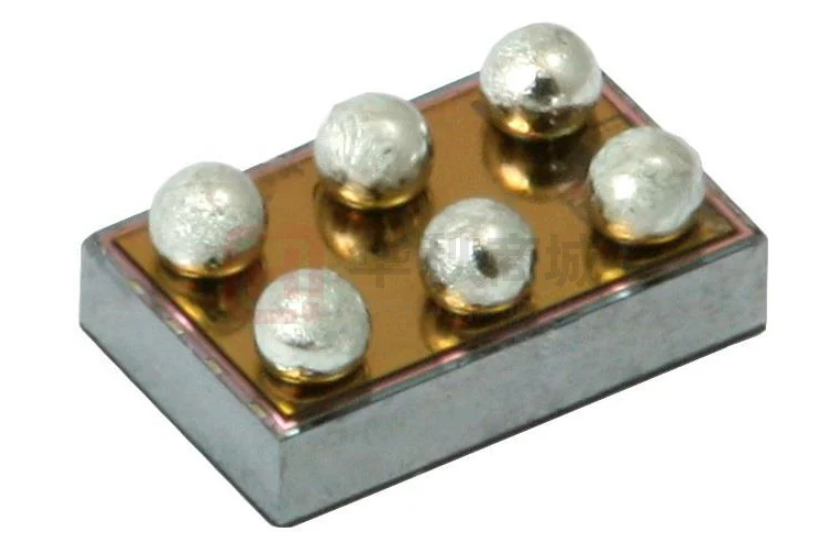
● Available in a 6-Bump WLP
The sensor communicates over a 1-Wire® bus that, by
definition, requires only one data line (and ground) for
communication with a microcontroller. In addition, the sensor can derive power directly from the data line (“parasite
power”), eliminating the need for an external power supply.
Each sensor has a unique 64-bit serial code, which allows
multiple MAX31825 ICs to reside on the same 1-Wire bus.
In addition, it includes two address input pins that, using
an external resistor and pin-strapping, allow one of 64 different addresses to be selected to identify each sensor's
physical location. Therefore, it is simple to use one microprocessor to control many devices distributed over a large
area.
The MAX31825 is available in a 6-bump WLP package.
The power supply voltage range is from 1.6V to 3.6V for
external power supplies, and from 2.3V to 3.6V for parasite power. The operating temperature range is from -45°C
to +145°C.
Applications
●
●
●
●
Industrial Equipment
Communications Equipment
Data Center Equipment
Consumer Equipment
19-100748; Rev 1; 10/20
Ordering Information appears at end of data sheet.
�1-Wire® Temperature Sensor with ±1ºC Accuracy
MAX31825
Typical Application Circuit
TO OTHER 1-WIRE DEVICES
VDD
VPU
VPU
4.7kΩ
4.7kΩ
I/O
DQ
ALARM
MCU
MAX31825
VDD
ADD0
GND
ADD1
RADD
www.maximintegrated.com
Maxim Integrated | 2
�MAX31825
1-Wire® Temperature Sensor with ±1ºC Accuracy
Absolute Maximum Ratings
VDD to GND.............................................................. -0.3V to +4V
ADD0, ADD1, ALARM, DQ to GND ......................... -0.3V to +4V
Continuous Power Dissipation (Multilayer Board, TA = +70°C,
derate 10.51mW/°C above +70°C)................................ 10.51mW
Operating Temperature Range ...........................-45°C to +145°C
Storage Temperature Range ..............................-60°C to +150°C
Soldering Temperature (reflow) ........................................ +260°C
Stresses beyond those listed under “Absolute Maximum Ratings” may cause permanent damage to the device. These are stress ratings only, and functional operation of the
device at these or any other conditions beyond those indicated in the operational sections of the specifications is not implied. Exposure to absolute maximum rating conditions for
extended periods may affect device reliability.
Package Information
WLP
Package Code
N61A1+1
Outline Number
21-100395
Land Pattern Number
N/A
Thermal Resistance, Four-Layer Board:
Junction to Ambient (θJA)
95.15°C/W
Junction to Case (θJC)
N/A
For the latest package outline information and land patterns (footprints), go to www.maximintegrated.com/packages. Note that a “+”, “#”, or “-” in the package code indicates
RoHS status only. Package drawings may show a different suffix character, but the drawing pertains to the package regardless of RoHS status.
Package thermal resistances were obtained using the method described in JEDEC specification JESD51-7, using a four-layer board. For detailed information on package thermal
considerations, refer to www.maximintegrated.com/thermal-tutorial.
www.maximintegrated.com
Maxim Integrated | 3
�1-Wire® Temperature Sensor with ±1ºC Accuracy
MAX31825
Electrical Characteristics
(TA = -40°C to +125°C, VDD = 1.6V to 3.6V, VPU = 2.3V to 3.6V, resolution = 12 bits, unless otherwise specified. Limits are 100%
tested at TA = +25°C. Limits over the operating temperature range and relevant supply voltage range are guaranteed by design and
characterization. )
PARAMETER
SYMBOL
CONDITIONS
Temperature
Measurement Error
-45°C to +145°C, 6-sigma
Conversion Time
10-bit (0.25°C) resolution
0°C to +70°C, 6-sigma
Temperature Resolution
MIN
TYP
MAX
-1.75
±0.3
+1.75
-1
+1
35
12 bits (Configuration bits D6:D5 = 11)
0.0625
10 bits (Configuration bits D6:D5 = 10)
0.25
9 bits (Configuration bits D6:D5 = 01)
0.5
8 bits (Configuration bits D6:D5 = 00)
1.0
80
UNITS
°C
ms
°C
°C
LOGIC DC CHARACTERISTICS
Local Power
Input Logic High Voltage
VIH
Parasite Power
Input Logic Low Voltage
VDD = 3.3V, VDD =
2.3V
VIL
Input High Leakage
Current
VDD x
0.7,
3.6
VDD x
0.8
V
VDD x
0.7,
3.6
VDD x
0.8
-0.5
Local Power, Excludes DQ
Input Low Leakage
Current
IIL
Input Capacitance
CIN
Output High Leakage
Current
Sink Current
VDD = 3.3V, VDD =
1.6V
VIN = 0V
-1
V
1
µA
+1
µA
5
VOUT = VDD
IL
±0.005
VDD x
0.2
VI/O = 0.4V
±0.005
VCC < 2.3V
2.5
VCC > 2.3V
4
pF
1
µA
mA
AC ELECTRICAL CHARACTERISTICS
POR Time
tPOR
Local or Parasite Power
3
Time to Strong Pullup
On
tSPON
Start Convert T command
10
Time Slot
tSLOT
60
10nF bypass capacitor from VCC to GND
8
ms
µs
120
4
µs
Recovery Time
TREC
Write-Zero Low Time
tLOW0
60
120
µs
µs
Write-One Low Time
tLOW1
4
15
µs
15
µs
Read Data Valid
tRDV
Reset Time High
tRSTH
480
µs
Reset Time Low
tRSTL
480
µs
Presence Detect High
tPDH
15
www.maximintegrated.com
60
µs
Maxim Integrated | 4
�1-Wire® Temperature Sensor with ±1ºC Accuracy
MAX31825
Electrical Characteristics (continued)
(TA = -40°C to +125°C, VDD = 1.6V to 3.6V, VPU = 2.3V to 3.6V, resolution = 12 bits, unless otherwise specified. Limits are 100%
tested at TA = +25°C. Limits over the operating temperature range and relevant supply voltage range are guaranteed by design and
characterization. )
PARAMETER
SYMBOL
CONDITIONS
MIN
TYP
UNITS
Presence Detect Low
tPDL
240
µs
DQ Capacitance
CDQ
Note 1
25
pF
Address Input
Capacitance
CADD
Note 1
2
pF
Time to Read Address
Selection Resistor
60
MAX
C ≤ 2pF
2
ms
POWER SUPPLY
Operating Supply
Voltage Range
Pullup Supply Voltage
Conversion Power
Supply Current
Average Power Supply
Current
Standby Supply Current
1.6
VPU
3.6
Parasite Power
2.3
3.6
Local Power
1.6
VDD
Active temperature conversions, DQ high
80
150
0.25 conversions/s,
10-bit (0.25°C)
resolution.
5
15
DQ high
V
V
µA
µA
4 conversions/s,
10-bit (0.25°C)
resolution.
9.8
24
In Standby, Parasite power, DQ = high
TA < +85ºC
2.5
6
µA
In Standby, Parasite Power, DQ = high
TA < +125ºC
2.5
12
μA
Note 1: Specifications are guaranteed by bench characterization and not automated test equipment (ATE) characterization.
www.maximintegrated.com
Maxim Integrated | 5
�MAX31825
1-Wire® Temperature Sensor with ±1ºC Accuracy
Typical Operating Characteristics
(TA = -40°C to +125°C, VDD = 1.6V to 3.6V, VPU = 2.3V to 3.6V, resolution = 12 bits, unless otherwise specified. Limits are 100%
tested at TA = +25°C. Limits over the operating temperature range and relevant supply voltage range are guaranteed by design and
characterization.)
www.maximintegrated.com
Maxim Integrated | 6
�1-Wire® Temperature Sensor with ±1ºC Accuracy
MAX31825
Pin Configuration
WLP
TOP VIEW
MAX31825ANT+
+
______
ALARM
B1
A1
DQ
ADD1
B2
A2
VDD
ADD0
B3
A3
GND
WLP
Pin Description
PIN
NAME
1
DQ
Data In/Out
2
VDD
External Parasite Power Capacitor and VDD Input. Connect a 3.3nF capacitor between this pin and
GND for parasite power operation. Connect power supply voltage to this pin when powering from
an external VDD source.
3
GND
Ground
5
ADD1
Address Selection Input. Connect to GND or VDD (DQ in parasite mode) to select the location
address.
4
ADD0
Address Selection Input. Connect a resistor to GND to select the location address.
6
ALARM
www.maximintegrated.com
FUNCTION
Alarm output. Open-drain. Note that the ALARM output generates alarm signals only in external
power mode.
Maxim Integrated | 7
�1-Wire® Temperature Sensor with ±1ºC Accuracy
MAX31825
Functional Diagram
PARASITE POWER
CIRCUIT
DQ
VDD
MAX31825
64-BIT
ROM
AND
1-WIRE
PORT
MEMORY
CONTROL LOGIC
10nF
TEMPERATURE SENSOR
ALARM LOW TRIGGER
(TL) REGISTER
CONFIGURATION REGISTER
8-BIT CRC REGISTER
www.maximintegrated.com
SCRATCHPAD
ALARM HIGH TRIGGER
(TH) REGISTER
GND
Maxim Integrated | 8
�MAX31825
1-Wire® Temperature Sensor with ±1ºC Accuracy
Detailed Description
The MAX31825 digital thermometer provides 12-bit temperature measurements and communicates over a 1-Wire bus
that by definition requires only one data line (and ground) for communication with a microcontroller. The data line requires
a weak pullup resistor since all devices are linked to the bus through a three-state or open-drain port (the MAX31825’s
DQ pin). Two address inputs (ADD0 and ADD1), simplify mapping of individual devices to specific locations.
Each 1-Wire device has a unique 64-bit serial code, allowing multiple devices to function on the same 1-Wire bus.
Therefore, it is simple to use one microcontroller to control many devices distributed over a large area. In this bus system,
the microcontroller identifies and addresses devices on the bus using each device’s unique 64-bit code. Because each
device has a unique code, the number of devices that can be addressed on one bus is virtually unlimited. The 1-Wire bus
protocol, including detailed explanations of the commands and time slots, is described in the 1-Wire Bus System section.
Control and data registers include the 2-byte temperature register that stores the digital output from the temperature
sensor, a configuration register for selecting operating modes, over-temperature and under-temperature alarm
thresholds, and a CRC register.
As an alternative to supplying power through the VDD pin, power can instead be supplied via the 1-Wire pullup resistor
through DQ when the bus is high. The high bus signal also charges an external capacitor (CPP), which then supplies
power to the device when the bus is low. This method of deriving power from the 1-Wire bus is referred to as parasite
power.
Measuring Temperature
Resolution is selectable to be 8, 9, 10, or 12 bits. 8-bit resolution corresponds to an LSB value of 1°C, while 12-bit
resolution corresponds to an LSB value of 0.0625°C. The sensor powers up in a low-power idle state. To initiate a single
temperature measurement, the master must issue a Convert T command, as described in Function Commands. The bus
requirements for parasite power are explained in the Powering the 1-Wire Temperature Sensor section.
When powered through VDD, automatic conversions may be selected using the Rate bits in the Configuration register.
When a rate other than 000 (standby) is selected, conversions take place at the selected rate, and the temperature
registers are updated at the end of each conversion. When parasite powered, the sensor ignores the Rate bits and
remains in standby mode until receiving a Convert T command.
The temperature data is stored as a 16-bit sign-extended two’s complement number in the temperature register (see
Temperature Data Format). The sign bit (S) indicate if the temperature is positive or negative. For positive numbers,
S = 0. For negative numbers, S = 1. Table 3 gives examples of digital output data and the corresponding temperature
readings.
www.maximintegrated.com
Maxim Integrated | 9
�1-Wire® Temperature Sensor with ±1ºC Accuracy
MAX31825
Powering the 1-Wire Temperature Sensor
The MAX31825 can be powered by an external supply connected to the VDD pin, or it can operate in “parasite power”
mode, which allows it to function without a local external supply. Parasite power is useful for applications that require
connection to the sensor through a cable, or those that are very space-constrained. Figure 1 shows the parasite-power
control circuitry, which “steals” power from the 1-Wire bus through DQ when the bus is high. The stolen charge powers
the sensor while the bus is high, and some of the charge is stored on the parasite-power capacitor (CPP) to provide
power when the bus is low.
In parasite-power mode, the 1-Wire bus and CPP can provide sufficient current for most operations as long as the
specified timing and voltage requirements are met (see the Logic DC Electrical Characteristics and AC Electrical
Characteristics sections of the Electrical Characteristics table). However, when performing temperature conversions, the
operating current can be as high as 150µA. This current can cause an unacceptable voltage drop across the 1-Wire
pullup resistor and is more current than can be supplied by CPP. To ensure that the sensor has sufficient supply current,
it is necessary to provide a strong pullup on the 1-Wire bus whenever temperature conversions are taking place. This
can be accomplished by using a MOSFET to pull the bus directly to the supply, as shown in Figure 1. The 1-Wire bus
must be switched to the strong pullup within 10µs (max) after issuing a Convert T command, and the bus must be held
high by the pullup for the duration of the conversion (tCONV). No other activity can take place on the 1-Wire bus while the
strong pullup is enabled.
The sensor can also be powered by the conventional method of connecting an external power supply to VDD, as shown
in Figure 2. The advantage of this method is that the MOSFET pullup is not required, and the 1-Wire bus is free to carry
other traffic during the temperature conversion period.
MAX31825
ADD0
VPU
MAX31825
VDD
ADD1
DQ
ALARM
GND
ADD0
ADD1
DQ
10nF
MAX31825
VDD
ALARM
GND
ADD0
VDD
ADD1
DQ
10nF
ALARM
GND
10nF
VPU
MCU
4.7kΩ
1-WIRE BUS
TO OTHER 1-WIRE DEVICES
Figure 1. Powering the MAX31825 from the 1-Wire Data Input (DQ)
VDD (EXTERNAL POWER)
MAX31825
VDD
MAX31825
MAX31825
ADD0
VDD
ADD0
VDD
ADD0
VDD
ADD1
ALARM
ADD1
ALARM
ADD1
ALARM
DQ
GND
1nF
DQ
GND
1nF
DQ
GND
1nF
VPU
MCU
4.7kΩ
1-WIRE BUS
TO OTHER 1-WIRE DEVICES
Figure 2. Powering the MAX31825 from an External Power Supply
www.maximintegrated.com
Maxim Integrated | 10
�MAX31825
1-Wire® Temperature Sensor with ±1ºC Accuracy
CPP Considerations for Parasite Power
When operating from parasite power, the values of CPP, pullup resistor RPU, and the pullup voltage VPU should be
chosen to work properly with the interface timing.
When system power is first connected, keep VDD high at least 5 time constants (5 x CPP x RPU) to fully charge CPP
before starting communications. For a single sensor with CPP = 10nF and RPU = 4.7kΩ, VDD should therefore stay high
for 77.55µs before starting communications. Note that if multiple 1-wire devices are on the bus, each will have its own
parasite power capacitor, and the total CPP will be the sum of the values of all of the parasite power capacitors. If the
total CPP is large, it may be useful to reduce the value of RPU to reduce the required VDD high period.
A 1-wire reset pulls DQ low for as long as 640µs. During this period, CPP must be large enough that the voltage across
it never falls below the 1.5V power-on-reset voltage. The maximum supply current (up to 125°C) in standby is 12µA. The
forward drop across the internal Ideal diode is nominally 50mV. Again using CPP = 10nF, a maximum standby supply
current of 12µA, and a maximum DQ reset low period of 640µs, we have a voltage drop on CPP of V = t x I/C = 640µs x
12µA/10nF = 582mV, which is compatible with the 2.3V specified minimum value of VPU.
www.maximintegrated.com
Maxim Integrated | 11
�1-Wire® Temperature Sensor with ±1ºC Accuracy
MAX31825
64-Bit ROM Code
Each 1-Wire component contains a unique 64-bit code stored in ROM (Figure 3). The least significant 8 bits of the ROM
code contain the sensor’s 1-Wire family code, 3Bh. The next 48 bits contain a unique serial number. The most significant
8 bits contain a cyclic redundancy check (CRC) byte that is calculated from the first 56 bits of the ROM code. See CRC
Generation for a detailed explanation of the CRC bits. The 64-bit ROM code and associated ROM function control logic
allow the device to operate as a 1-Wire device using the protocol detailed in 1-Wire Bus System.
MSB
LSB
8-BIT CRC CODE
MSB
48-BIT SERIAL NUMBER
LSB MSB
8-BIT FAMILY
CODE (3Bh)
LSB MSB
LSB
Figure 3. 64-bit ROM Code
www.maximintegrated.com
Maxim Integrated | 12
�MAX31825
1-Wire® Temperature Sensor with ±1ºC Accuracy
Address
Although the 64-bit ROM code allows each 1-Wire device on a bus to be identified for communication purposes, it does
not provide any information about the location of the device. The MAX31825 includes two address pins (ADD0 and
ADD1). ADD0 can be connected to an external resistor whose value is measured by the MAX31825 in response to the
Convert Location command, resulting in five location address bits (A4:A0) being stored in the Status register. Because
the location resistor values on the board are known, this location address allows the location of the MAX31825 to be
uniquely identified. Mapping of the address selection resistor value to A4:A0 is shown in Table 1. In addition to ADD0, the
ADD1 input can be connected to GND or VDD (or DQ in parasite-power mode). This selects the value of bit A5, yielding
a total of 64 available addresses. A5 = 1 when ADD1 is connected to VDD and 0 when ADD1 is grounded.
Table 1. Resistor Selection of Address bits A4:A0
A4:A0
1% RESISTOR VALUE
(kΩ)
11111
4.2
11110
5
11101
5.9
11100
7.1
11011
8.4
11010
10
11001
11.9
11000
14.1
10111
16.8
10110
20
10101
23.8
10100
28.3
10011
33.6
10010
40
10001
47.6
10000
56.6
01111
67.3
01110
80
01101
95.1
01100
113.1
01011
134.5
01010
160
01001
190.3
01000
226.3
00111
269.1
00110
320
00101
380.5
00100
452.5
00011
538.2
00010
640
www.maximintegrated.com
Maxim Integrated | 13
�1-Wire® Temperature Sensor with ±1ºC Accuracy
MAX31825
Table 1. Resistor Selection of Address bits A4:A0 (continued)
A4:A0
1% RESISTOR VALUE
(kΩ)
00001
761.1
00000
905.1
Control and Data Registers
The control and data registers are organized as shown in Table 2. All memory commands are described in detail in the
Function Commands section.
Table 2. Register Functions
BYTE ADDRESS
READ OR WRITE
0
R
Temperature LSB (+85°C)
1
R
Temperature MSB (+85°C)
2
R
Status [TH, TL state, address]
3
R/W
Configuration
4
R/W
TH MSB (+128°C)
5
R/W
TH LSB (+128°)
6
R/W
TL LSB (-55°)
7
R/W
TL MSB (-55°)
8
R
www.maximintegrated.com
BYTE FUNCTION (POWER-UP STATE)
CRC
Maxim Integrated | 14
�1-Wire® Temperature Sensor with ±1ºC Accuracy
MAX31825
Temperature Data
Byte 0 and byte 1 contain the least significant byte and the most significant byte of the temperature register, respectively.
Two different formats are available: Normal and Extended. Normal format produces temperature data up to 128°C 1LSB, and Extended format produces data up to and beyond the 145°C operating limit.
Table 3. Temperature Data Format (S = Sign Bit)
MOST SIGNIFICANT BYTE (°C)
LEAST SIGNIFICANT BYTE (°C)
COMMENT
D7
D6
D5
D4
D3
D2
D1
D0
D7
D6
D5
D4
D3
D2
D1
D0
S
S
S
S
S
64
32
16
8
4
2
1
0.5
0.25
0.125
0.0625
S
S
S
S
128
64
32
16
8
4
2
1
0.5
0.25
0.125
0.0625
Normal format
Extended format
Table 4. Temperature/Data Relationship. Shown for 12-bit Resolution.
TEMPERATURE
(°C)
NORMAL FORMAT
DATA (BINARY)
NORMAL FORMAT
DATA (HEX)
EXTENDED FORMAT
DATA (BINARY)
EXTENDED FORMAT
DATA (HEX)
+150
+128
0000 0111 1111 1111
07FF
0000 1001 0110 0000
0960h
0000 0111 1111 1111
07FFh
0000 1000 0000 0000
0800h
+125
0000 0111 1101 0000
07D0h
0000 0111 1101 0000
07D0h
+85
0000 0101 0101 0000
0550h
0000 0101 0101 0000
0550h
+25.0625
0000 0001 1001 0001
0191h
0000 0001 1001 0001
0191h
+10.125
0000 0000 1010 0010
00A2h
0000 0000 1010 0010
00A2h
+0.5
0000 0000 0000 1000
0008h
0000 0000 0000 1000
0008h
0
0000 0000 0000 0000
0000h
0000 0000 0000 0000
0000h
-0.5
1111 1111 1111 1000
FFF8h
1111 1111 1111 1000
FFF8h
-10.125
1111 1111 0101 1110
FF5E
1111 1111 0101 1110
FFF8h
-25.0625
1111 1110 0110 1111
FE6Fh
1111 1110 0110 1111
FE6Fh
-55
1111 1100 1001 0000
FC90h
1111 1100 1001 0000
FC90h
Status Register
The Status register contains the overtemperature (TH) and undertemperature (TL) status bits and the location bits. The
A[5:0] bits report the address information selected by the resistor value at ADD0 and the logic state of ADD1. Initiate a
Detect Address command to measure the external resistor value and populate these bits. The default value is all 0s.
Table 5. Status Register Format
BIT
7
6
5
4
3
2
1
FUNCTION
TH FAULT
TL FAULT
A5
A4
A3
A2
A1
DEFAULT
0
0
0
0
0
0
0
www.maximintegrated.com
0
A0
0
Maxim Integrated | 15
�1-Wire® Temperature Sensor with ±1ºC Accuracy
MAX31825
Configuration Register
Byte 3 contains the configuration register, which is organized as shown in Table 6. The configuration register provides
control over several operating parameters, including data format, conversion resolution, the ALARM output mode, and
the continuous conversion rate.
Table 6. Configuration Register Format
BIT
7
6
5
4
3
2
1
0
FUNCTION
Format
Res 1
Res 0
Comp/Int
Reserved
Rate 2
Rate 1
Rate 0
DEFAULT
0
1
1
1
0
0
0
0
Temperature Data Format
As discussed in the Temperature Data section, Bit 7 of the Configuration register selects the temperature data format.
When D7 is 0 (normal format), the data format is two’s complement with a range of -128°C to (128°C - 1LSB), where the
value of an LSB depends on the resolution selection. Write a 1 to bit 7 for extended temperature format. In extended
format, the MSB is given a value of 128°C, which allows temperatures as high as 145°C to be measured. After changing
the value of bit 7 the data format does not update until the completion of the following temperature conversion. After
setting bit 7 to 1, new extended temperature data is guaranteed ready after a period equal to twice the maximum
conversion time. Note that changing the data format bit does not change the format of the values in the TH and TL
registers; these values must be written to the registers in the format selected by Bit 7.
Resolution
The resolution bits (D6:D5) select the conversion resolution. The conversion time doubles with every bit of increased
resolution. for example, the nominal 10-bit conversion time is 35ms. Increasing the resolution to 12 bits increases the
conversion time to 140ms. The resolution bits allow resolution, conversion time, and average supply current to be
optimized for the application's requirements.
Table 7. Resolution Selection
D6
D5
RESOLUTION (BITS)
0
0
8
0
1
9
1
0
10
1
1
12 (default)
Comparator/Interrupt
Set bit D4, the COMPARATOR/INTERRUPT bit, to 0 to make the ALARM output and the Overtemperature and
Undertemperature Status bits operate in Comparator mode. In Comparator mode, the ALARM output asserts and the
Status bit is set to 1 when the temperature rises above the TH value or falls below the TL value. The ALARM output
de-asserts and the Status bits return to 0 when the measured temperature returns to a value ranging from TH to TL.
Set bit D4 to 1 to operate the ALARM output and Status bits in interrupt mode. In interrupt mode, exceeding TH or going
below TL also asserts the ALARM output and sets the Status bits to 1. ALARM remains asserted and the Status bits
remain set to 1 until a read operation is performed on any of the registers, at which point ALARM is de-asserted and the
Status bits return to 0. Note that if the result of the next conversion is greater than TH or less than TL, the ALARM output
will assert and the Status bit(s) will set.
Note that the ALARM output functions only in external power mode.
www.maximintegrated.com
Maxim Integrated | 16
�1-Wire® Temperature Sensor with ±1ºC Accuracy
MAX31825
Conversion Rate
The conversion rate bits, D2:D0, select the rate for automatic continuous conversions. These bits apply only when
external power is used; they must be set to 000 when operating in parasite power mode. Rates from approximately
one sample per minute to 8sps are available, as well as 0sps (or Standby). The nominal conversion time is 35ms
at a resolution of 10 bits, with the conversion time changing by a factor of two for each bit of resolution change. In
automatic conversion mode, available only when VDD is connected to a power supply, conversions are started at the
selected rate and shutdown mode is entered between conversions to reduce average power supply current. Note that the
highest conversion rate can't be achieved at 12-bit resolution. When the conversion rate bits are set to 000, the ConvertT
command initiates a single conversion and a return to shutdown. When the bits are set to a different value, the ConvertT
command initiates continuous conversions. Continuous conversions may be stopped or the rate may be changed by
changing the value of the conversion rate bits.
Conversion Rate Selection
D2
D1
D0
CONVERSION RATE
0
0
0
0 (Shutdown)
0
0
1
1 conversion/64 second
0
1
0
1 conversion/32 second
0
1
1
1 conversion/16 second
1
0
0
1 conversion/4 second
1
0
1
1 conversion/second
1
1
0
4 conversion/second
1
1
1
8 conversion/second
Alarm Thresholds
Bytes 4 through 7 contain the 16-bit alarm thresholds TH and TL. The default value of TH is 160°C, and the default value
of TL is -65°C. The data format is the same as that of the temperature register.
CRC
Byte 8 is read-only and contains the CRC code for bytes 0–7 of the scratchpad. The sensor generates this CRC using
the method described in CRC Generation.
www.maximintegrated.com
Maxim Integrated | 17
�1-Wire® Temperature Sensor with ±1ºC Accuracy
MAX31825
CRC Generation
CRC bytes are provided as part of the device’s 64-bit ROM code, in the 9th byte of the Scratchpad. The ROM code
CRC is calculated from the first 56 bits of the ROM code and is contained in the most significant byte of the ROM. The
scratchpad CRC is calculated from the data in the scratchpad, and therefore changes when the data in the scratchpad
changes. The CRC provides the bus master with a method of data validation when data is read from the device. To verify
that data has been read correctly, the bus master must recalculate the CRC from the received data and then compare this
value to either the ROM code CRC (for ROM reads) or to the scratchpad's CRC (for scratchpad reads). If the calculated
CRC matches the read CRC, the data has been received error-free. The comparison of CRC values and the decision to
continue with an operation are determined entirely by the bus master. There is no circuitry inside the device that prevents
a command sequence from proceeding if the CRC (ROM or scratchpad) does not match the value generated by the bus
master.
The equivalent polynomial function of the CRC (ROM or scratchpad) is:
CRC = X8 + X5 + X4 + 1
The bus master can recalculate the CRC and compare it to the CRC values from the device using the polynomial
generator shown in Figure 4. This circuit consists of a shift register and XOR gates, and the shift register bits are
initialized to 0. Starting with the least significant bit of the ROM code or the least significant bit of byte 0 in the scratchpad,
one bit at a time should shifted into the shift register. After shifting in the 56th bit from the ROM or the most significant
bit of byte 7 from the Scratchpad 1 or byte 10 from Scratchpad 2, the polynomial generator contains the recalculated
CRC. Next, the 8-bit ROM code or scratchpad CRC from the device must be shifted into the circuit. At this point, if the
recalculated CRC was correct, the shift register contains all zeros. Additional information about the Maxim 1-Wire CRC
is available in Application Note 27: Understanding and Using Cyclic Redundancy Checks with Maxim iButton® Products.
POLYNOMIAL = X8 + X5 + X4 + 1
1ST
STAGE
X0
3rd
STAGE
2nd
STAGE
X1
X2
4th
STAGE
X3
6th
STAGE
5th
STAGE
X4
X5
7th
STAGE
X6
8th
STAGE
X7
X8
INPUT DATA
Figure 4. CRC Polynomial Generator
www.maximintegrated.com
Maxim Integrated | 18
�1-Wire® Temperature Sensor with ±1ºC Accuracy
MAX31825
1-Wire Bus System
The 1-Wire bus system uses a single bus master to control one or more slave devices. The temperature sensor is always
a slave. When there is only one slave on the bus, the system is referred to as a single-drop system; the system is
multidrop if there are multiple slaves on the bus. All data and commands are transmitted least significant bit first over the
1-Wire bus.
The following discussion of the 1-Wire bus system is broken down into three topics: hardware configuration, transaction
sequence, and 1-Wire signaling (signal types and timing).
1-WIRE WRITE-ZERO TIME SLOT
START OF NEXT CYCLE
tSLOT
tREC
tLOW0
1-WIRE READ-ZERO TIME SLOT
tSLOT
START OF NEXT CYCLE
tREC
tRDV
1-WIRE RESET PULSE
RESET PULSE FROM HOST
tRSTL
tRSTH
1-WIRE PRESENCE DETECT
PRESENCE DETECT
tPDHIGH
tPDLOW
Figure 5. 1-Wire Bus Timing Diagram
www.maximintegrated.com
Maxim Integrated | 19
�1-Wire® Temperature Sensor with ±1ºC Accuracy
MAX31825
Hardware Configuration
The 1-Wire bus has by definition only a single data line. Each device (master or slave) interfaces to the data line by using
an open-drain or three-state port. This allows each device to “release” the data line when the device is not transmitting
data, thereby making the bus available for use by another device. The device’s 1-Wire port (DQ) is open drain with an
internal circuit equivalent to that shown in Figure 6.
The 1-Wire bus requires an external pullup resistor of approximately 5kΩ; thus, the idle state for the 1-Wire bus is high. If
for any reason a transaction needs to be suspended, the bus must be left in the idle state if the transaction is to resume.
Infinite recovery time can occur between bits so long as the 1-Wire bus is in the inactive (high) state during the recovery
period. If the bus is held low for more than 480µs, all components on the bus are reset.
VPU
BUS MASTER
4.7kΩ
TO OTHER 1-WIRE DEVICES
Rx
1-WIRE BUS
DQ
Tx
OPEN DRAIN
OUTPUT
MAX31825
5µA
TYPICAL
Rx
Tx
Figure 6. Hardware Configuration
Transaction Sequence
The transaction sequence for accessing the device is as follows:
Step 1: Initialization
Step 2: ROM Command (followed by any required data exchange)
Step 3: Function Command (followed by any required data exchange)
It is very important to follow this sequence every time the MAX31825 is accessed, as the MAX31825 does not respond
if any steps in the sequence are missing or out of order. An exception to this rule is the Search ROM command. After
issuing this ROM command, the master must return to step 1 in the sequence.
Initialization
All transactions on the 1-Wire bus begin with an initialization sequence. The initialization sequence consists of a reset
pulse transmitted by the bus master followed by presence pulse(s) transmitted by the slave(s). The presence pulse lets
the bus master know that slave devices (MAX31825) are on the bus and are ready to operate. Timing for the reset and
presence pulses is detailed in 1-Wire Signaling.
www.maximintegrated.com
Maxim Integrated | 20
�1-Wire® Temperature Sensor with ±1ºC Accuracy
MAX31825
ROM Commands
After the bus master has detected a presence pulse, it can issue a ROM command. These commands operate on the
unique 64-bit ROM codes of each slave device and allow the master to single out a specific device if many are present on
the 1-Wire bus. These commands also allow the master to determine how many and what types of devices are present on
the bus. There are four ROM commands, and each command is 8 bits long. The master device must issue an appropriate
ROM command before issuing a MAX31825 function command. An exception to the rule is when detect address is used
to communicate with devices. ROM commands are not used when selecting an address to communicate. Figure 7 shows
a flowchart for operation of the ROM commands.
MASTER Tx RESET PULSE
INITIALIZATION SEQUENCE
MAX31825 Tx PRESENCE PULSE
MASTER Tx ROM COMMAND
N
33h READ ROM?
Y
N
55h MATCH ROM?
N
F0h SEARCH ROM?
Y
Y
N
N
CCh SKIP ROM?
Y
ADDRESSES
PREVIOUSLY
DETECTED?
Y
MAX31825 Tx BIT 0
MAX31825 Tx
FAMILY CODE BYTE
MASTER Tx BIT 0
MAX31825 Tx BIT 0
MASTER Tx BIT 0
BIT 0 MATCH?
N
N
BIT 0 MATCH?
Y
Y
MAX31825 Tx SERIAL
NUMBER (6 BYTES)
MAX31825 Tx BIT 1
MASTER Tx BIT 1
MAX31825 Tx BIT 1
MASTER Tx BIT 1
BIT 1 MATCH?
N
N
BIT 1 MATCH?
MAX31825 Tx CRC BYTE
Y
Y
MAX31825 Tx BIT 63
MAX31825 Tx BIT 63
MASTER Tx BIT 63
MASTER Tx BIT 63
BIT 63 MATCH?
Y
N
N
BIT 63 MATCH?
Y
MASTER Tx
FUNCTION COMMAND
Figure 7. MAX31825 ROMs Command Flowchart
www.maximintegrated.com
Maxim Integrated | 21
�MAX31825
1-Wire® Temperature Sensor with ±1ºC Accuracy
Search ROM [F0h]
When a system is initially powered up, the master must identify the ROM codes of all slave devices on the bus, which
allows the master to determine the number of slaves and their device types. The master learns the ROM codes through
a process of elimination that requires the master to perform a Search ROM cycle (i.e., Search ROM command followed
by data exchange) as many times as necessary to identify all the slave devices. If there is only one slave on the bus, the
simpler Read ROM command can be used in place of the Search ROM process. For a detailed explanation of the Search
ROM command procedure, refer to Application Note 937: Book of iButton® Standards. After every Search ROM cycle,
the bus master must return to step 1 (initialization) in the transaction sequence.
Read ROM [33h]
This command can be used only when there is one slave on the bus. It allows the bus master to read the slave’s 64-bit
ROM code without using the Search ROM command procedure. If this command is used when there is more than one
slave present on the bus, a data collision occurs when all the slaves attempt to respond at the same time.
Match ROM [55h]
The Match ROM command followed by a 64-bit ROM code sequence allows the bus master to address a specific slave
device on a multidrop or single-drop bus. Only the slave that exactly matches the 64-bit ROM code sequence responds
to the function command issued by the master; all other slaves on the bus wait for a reset pulse.
Skip ROM [CCh]
The master can use this command to address all devices on the bus simultaneously without sending out any ROM code
information. For example, the master can make all devices on the bus perform simultaneous temperature conversions by
issuing a Skip ROM command followed by a Convert T function command.
Note that the Read Scratchpad command can follow the Skip ROM command only if there is a single slave device on the
bus. In this case, time is saved by allowing the master to read from the slave without sending the device’s 64-bit ROM
code. A Skip ROM command followed by a Read Scratchpad command causes a data collision on the bus if there is
more than one slave because multiple devices attempt to transmit data simultaneously.
www.maximintegrated.com
Maxim Integrated | 22
�1-Wire® Temperature Sensor with ±1ºC Accuracy
MAX31825
Function Commands
After the bus master has used a ROM command to address the unit with which it wishes to communicate, the master can
issue one of the available function commands. These commands allow the master to read from the device’s scratchpad
memory, and initiate temperature conversions. The function commands are summarized in Table 8 and illustrated by the
flowchart in Figure 8.
Table 8. Function Commands Summary
COMMAND
DESCRIPTION
PROTOCOL
1-WIRE BUS ACTIVITY AFTER COMMAND IS ISSUED
Convert T
Initiates temperature
conversion.
44h
The MAX31825 transmits conversion status to master (not
applicable for parasite-powered devices).
Read
Scratchpad
Reads the 9-byte scratchpad
including the CRC byte.
BEh
The MAX31825 transmits up to 9 data bytes to master. The 9th byte
is the CRC byte.
Write
Scratchpad
Writes bytes 3 through 7
(Configuration and thresholds)
to the scratchpad.
4Eh
The master transmits five bytes to the scratchpad.
Detect
Address
Loads location bits
88h
The MAX31825 measures the external resistor value and writes
location bits to Status register.
Select
Address
Selects device with location bits
that match transmitted bits.
Follow with a Convert, Read, or
Write command.
70h
Host transmits desired location bits to devices on the bus, then
transmits another Function Command (Read, Write, or Convert).
Only the MAX31825 with the transmitted location bits responds to
the second Function Command.
www.maximintegrated.com
Maxim Integrated | 23
�1-Wire® Temperature Sensor with ±1ºC Accuracy
MAX31825
MASTER Tx
FUNCTION COMMAND
4Eh WRITE
SCRATCHPAD?
N
44h CONVERT??
Y
N
BEh READ
SCRATCHPAD?
Y
PARASITE POWER?
MAX31825 BEGINS
CONVERSION
N
Y
MASTER ENABLES
STRONG PULLUP ON DQ
N
Y
MASTER Tx
CONFIGURATION BYTE
MASTER Rx DATA BYTE
MASTER Tx TH BYTES
MASTER Tx RESET?
Y
N
CONVERTING
TEMPERATURE?
MASTER Tx TL BYTES
MAX31825 CONVERTS
TEMPERATURE
N
N
Y
MASTER Rx“0s”
HAVE 8 BYTES
BEEN READ?
Y
MASTER Rx“1s”
N
MASTER DISABLES
STRONG PULLUP
70h SELECT
ADDRESS?
Y
MASTER Tx DEVICE
ADDRESS AND FUNCTION
COMMAND
N
Rx ADDRESS
MATCHES STATUS
5:0?
Y
MASTER Rx SCRATCHPAD
CRC BYTE
N
88h DETECT
ADDRESS?
Y
MAX31825 MEASURES
RADD
MAX31825 DETECTS
ADDRESS
MAX31825 WRITES
ADDRESS TO STATUS
EXECUTE Rx FUNCTION
COMMAND
WAIT FOR
NEXTINITIALIZATION
SEQUENCE
Figure 8. MAX31825 Function Commands Flowchart
www.maximintegrated.com
Maxim Integrated | 24
�MAX31825
1-Wire® Temperature Sensor with ±1ºC Accuracy
Convert T [44h]
This command initiates a single temperature conversion. Following the conversion, the resulting thermal data is stored
in the 2-byte temperature register in the Scratchpad memory and the sensor returns to its low-power idle state. If used
in parasite-power mode, within 10µs (max) after this command is issued, the master must enable a strong pullup on the
1-Wire bus for the duration of the conversion (tCONV), as described in Powering the 1-Wire Temperature Sensor. If the
sensor is powered by an external supply, the master can issue read time slots after the Convert T command, and the
sensor responds by transmitting 0 while the temperature conversion is in progress and 1 when the conversion is done.
In parasite-power mode, this notification technique cannot be used because the bus is pulled high by the strong pullup
during the conversion.
When in automatic conversion mode, Convert T is ignored if a conversion is in progress. After performing a convert T the
MAX31825 returns to standby or automatic conversions, whichever was in effect before the command was given.
Write Scratchpad (4Eh)
Writes bytes 3 through 7 (Configuration and thresholds) to the scratchpad.
Read Scratchpad [BEh]
This command allows the master to read the contents of the Scratchpad. The data transfer starts with the least significant
bit of byte 0 and continues through the scratchpad until the 9th byte (byte 8, CRC) is read. The master can issue a reset
to terminate reading at any time if only part of the scratchpad data is needed. The CRC is computed while data is read
from bytes 0–7, and is shifted out as byte 8.
Detect Address [88h]
The MAX31825 measures the external resistor value and writes location bits to Status register.
Select Address [70h]
The Select Address command allows faster transaction sequences by bypassing the 64-bit ROM code, while still
identifying a unique MAX31825 on the bus. The resistor connected to the ADD0 and ADD1 input determines the values
of the six least-significant address bits in the Status register. The Select Address command selects the unit with location
bits that match the bit transmitted by the host. The operation sequence is as follows:
1. Initialization sequence
2. The host transmits the Select Address command, followed by the desired address bits to devices on the bus. The
address bits are transmitted as the six LSBs of a byte whose remaining bits are set to 0.
3. The host then transmits another Function Command (Read, Write, or Convert). Only the MAX31825 with the location
bits equal to the values transmitted in step 2 responds to this command.
Note that this command may be used only when each MAX31825 on the bus has a unique address. If multiple sensors
share an address, collisions will occur.
1-Wire Signaling
Using a strict 1-Wire communication protocol helps to ensure data integrity. Several signal types are defined by this
protocol: reset pulse, presence pulse, write-zero, write-one, read-zero, and read-one. The bus master initiates all these
signals except the presence pulse.
www.maximintegrated.com
Maxim Integrated | 25
�1-Wire® Temperature Sensor with ±1ºC Accuracy
MAX31825
Initialization Procedure: Reset and Presence Pulses
All communication with the device begins with an initialization sequence that consists of a reset pulse from the master
followed by a presence pulse from the device (illustrated in Figure 9). When the device sends the presence pulse in
response to the reset, it is indicating to the master that it is on the bus and ready to operate.
During the initialization sequence, the bus master transmits (Tx) the reset pulse by pulling the 1-Wire bus low for 480µs
(min). The bus master then releases the bus and goes into receive mode (Rx). When the bus is released, the pullup
resistor pulls the 1-Wire bus high. When the device detects this rising edge, it waits 15µs to 60µs and then transmits a
presence pulse by pulling the 1-Wire bus low for 60µs to 240µs.
MASTER Rx
480µs MINIMUM
MASTER Tx RESET PULSE
480µs MINIMUM
MAX31825 WAITS
15µs TO 60µs
VPU
MAX31825 Tx PRESENCE
PULSE 60µs TO 240µs
1-Wire BUS
GND
BUS MASTER PULLING LOW
MAX31825 PULLING LOW
RESISTOR PULLUP
Figure 9. Initialization Timing
Read/Write Time Slots
The bus master writes data to the device during write time slots and reads data from the device during read time slots.
One bit of data is transmitted over the 1-Wire bus per time slot.
www.maximintegrated.com
Maxim Integrated | 26
�1-Wire® Temperature Sensor with ±1ºC Accuracy
MAX31825
Write Time Slots
There are two types of write time slots: write-one time slots and write-zero time slots. The bus master uses a write-one
time slot to write a logic 1 to the device and a write-zero time slot to write a logic 0 to the device. All write time slots must
have a 60µs (min) duration with a 1µs (min) recovery time between individual write slots. Both types of write time slots
are initiated by the master pulling the 1-Wire bus low Figure 10.
To generate a write-one time slot, after pulling the 1-Wire bus low, the bus master must release the 1-Wire bus within
15µs. When the bus is released, the pullup resistor pulls the bus high. To generate a write-zero time slot, after pulling the
1-Wire bus low, the bus master must continue to hold the bus low for the duration of the time slot (at least 60µs).
The device samples the 1-Wire bus during a window that lasts from 15µs to 60µs after the master initiates the write time
slot. If the bus is high during the sampling window, a 1 is written to the device. If the line is low, a 0 is written to the device.
STARTOF SLOT
STARTOF SLOT
MASTER WRITE-ZERO SLOT
MASTER WRITE-ONE SLOT
1µs < tREC < ∞
60µs < Tx “0” < 120µs
> 1µs
VPU
1-WIRE BUS
GND
MAX31825 SAMPLES
MIN
15µs
TYP
15µs
MAX31825 SAMPLES
MAX
MIN
30µs
15µs
MASTER READ-ZERO SLOT
TYP
15µs
MAX
30µs
MASTER READ-ONE SLOT
1µs < tREC < ∞
VPU
1-Wire BUS
GND
MASTER SAMPLES
> 1µs
MASTER SAMPLES
> 1µs
15µs
45µs
BUS MASTER PULLING LOW
15µs
MAX31825 PULLING LOW
RESISTOR PULLUP
Figure 10. Read/Write Time Slot Timing Diagram
www.maximintegrated.com
Maxim Integrated | 27
�1-Wire® Temperature Sensor with ±1ºC Accuracy
MAX31825
Read Time Slots
The device can only transmit data to the master when the master issues read time slots. Therefore, the master must
generate read time slots immediately after issuing a Read Scratchpad command, so that the device can provide the
requested data. In addition, the master can generate read time slots after issuing a Convert T command to verify the
operation status, as explained in Function Commands.
All read time slots must be 60µs (min) in duration with a 1µs (min) recovery time between slots. A read time slot is initiated
by the master device pulling the 1-Wire bus low for a minimum of 1µs (tINIT) and then releasing the bus (Figure 10). After
the master initiates the read time slot, the device begins transmitting a 1 or 0 on bus. The device transmits a 1 by leaving
the bus high and transmits a 0 by pulling the bus low. When transmitting a 0, the device releases the bus by the end of
the time slot, and the pullup resistor pulls the bus back to its high idle state. Output data from the device is valid for 15µs
after the falling edge that initiated the read time slot. Therefore, the master must release the bus and then sample the
bus state within 15µs from the start of the slot. Figure 11 illustrates that the sum of tINIT, tRC, and the master sample
window must be less than 15µs for a read time slot. tRC is the rise time due to the resistive and capacitive characteristics
of the bus. Figure 12 shows that system timing margin is maximized by keeping tINIT and tRC as short as possible and
by locating the master sample time during read time slots near the end of the 15µs period.
VPU
VIH OF MASTER
1-WIRE BUS
GND
tINIT > 1µs
tRC
MASTER SAMPLES
15µs
BUS MASTER PULLING LOW
RESISTOR PULLUP
Figure 11. Detailed Master Read-One Timing
VPU
VIH OF MASTER
1-WIRE BUS
GND
tINIT =
SMALL
tRC =
SMALL
MASTER SAMPLES
15µs
BUS MASTER PULLING LOW
RESISTOR PULLUP
Figure 12. Recommended Master Read-One Timing
www.maximintegrated.com
Maxim Integrated | 28
�MAX31825
1-Wire® Temperature Sensor with ±1ºC Accuracy
Ordering Information
PART NUMBER
TEMPERATURE RANGE
PIN-PACKAGE
MAX31825ANT+
-40°C to +125°C
6-WLP
+ Denotes a lead(Pb)-free/RoHS-compliant package.
T = Tape and reel.
www.maximintegrated.com
Maxim Integrated | 29
�1-Wire® Temperature Sensor with ±1ºC Accuracy
MAX31825
Revision History
REVISION
NUMBER
REVISION
DATE
PAGES
CHANGED
DESCRIPTION
0
2/20
Initial Release
1
10/20
Updated Benefits and Features, Electrical Characteristics, and Detailed Description
—
1, 4, 5, 16, 17
For pricing, delivery, and ordering information, please visit Maxim Integrated’s online storefront at https://www.maximintegrated.com/en/storefront/storefront.html.
Maxim Integrated cannot assume responsibility for use of any circuitry other than circuitry entirely embodied in a Maxim Integrated product. No circuit patent
licenses are implied. Maxim Integrated reserves the right to change the circuitry and specifications without notice at any time. The parametric values (min and max
limits) shown in the Electrical Characteristics table are guaranteed. Other parametric values quoted in this data sheet are provided for guidance.
Maxim Integrated and the Maxim Integrated logo are trademarks of Maxim Integrated Products, Inc.
© 2020 Maxim Integrated Products, Inc.
�