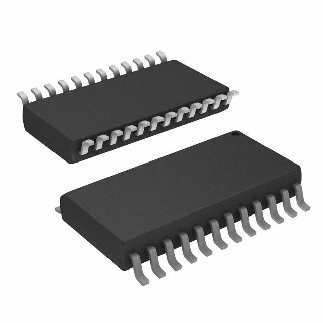
MAX335
Serial Controlled, 8-Channel SPST Switch
General Description
The MAX335 analog switch with serial digital interface
offers eight separately controlled single-pole-single-throw
(SPST) switches. All switches conduct equally in either
direction, and on-resistance (100Ω) is constant over the
analog signal range.
These CMOS switches can operate continuously with
power supplies ranging from ±4.5V to ±20V and handle
rail-to-rail analog signals. Upon power-up, all switches are
off, and the internal serial and parallel shift registers are
reset to zero. The MAX335 is equivalent to two DG211
quad switches but controlled by a serial interface.
Features
●● 8 Separately Controlled SPST Switches
●● SPI-Compatible Serial Interface
●● Accepts ±15V Analog Swings
●● Multiple Devices Can Be Daisy-Chained
Ordering Information
PART
TEMP RANGE
PIN-PACKAGE
MAX335CNG
0°C to +70°C
24 Narrow Plastic DIP
MAX335CWG
0°C to +70°C
24 Wide SO
The interface is compatible with the Motorola SPI interface
standard. Functioning as a shift register, this serial interface
allows data (at DIN) to be locked in synchronous with the
rising edge of clock (SCLK). The shift register’s output
(DOUT) enables several MAX335s to be daisy chained.
MAX335C/D
0°C to +70°C
Dice*
MAX335ENG
-40°C to +85°C
24 Narrow Plastic DIP
MAX335EUG
-40°C to +85°C
24 TSSOP
MAX335EWG
-40°C to +85°C
24 Wide SO
Applications
MAX335MRG
-55°C to +125°C
24 Narrow CERDIP**
●●
●●
●●
●●
Serial Data Acquisition and Process Control
Avionics
Signal Routing
Networking
*Contact factory for dice specifications.
**Contact factory for availability and processing to MIL-STD-883.
Pin Configuration
NO7
NO0
TOP VIEW
SCLK 1
COM0
COM7
+
24 CS
V+ 2
23 VL
DIN 3
GND 4
PARALLEL REGISTER AND TRANSLATOR
22 DOUT
MAX335
NO0 5
20 NO7
COM0 6
DIN
DOUT
8-BIT SHIFT REGISTER
19 COM7
NO1 7
18 NO6
COM1 8
VL
CLOCK TRANSLATOR
CS TRANSLATOR
19-0220; Rev 4; 7/17
15 COM5
NO3 11
14 NO4
COM3 12
LATCH
CS
16 NO5
COM2 10
MAX335
SCLK
17 COM6
NO2 9
+5V TRANSLATOR
21 V-
13 COM4
DIP/SO
�MAX335
Serial Controlled, 8-Channel SPST Switch
Absolute Maximum Ratings
Voltages Referenced to VV+.......................................................................................44V
GND....................................................................................25V
VL................................................. (GND - 0.3V) to (V+ + 0.3V)
SCLK, CS, DIN, DOUT, NO_, COM_............V- -2V to V+ +2V
or 30mA, whichever occurs first
Continuous Current (any terminal)......................................30mA
Peak Current, NO or COM
(pulsed at 1ms, 10% duty cycle MAX)............................00mA
Continuous Power Dissipation (TA = +70°C) (Note 1)
Narrow Plastic DIP
(derate 13.33mW/°C above +70°C)...........................1067mW
Wide SO (derate 11.76mW/°C above +70°C)..............941mW
Narrow CERDIP (derate 12.50mW/°C above +70°C)....1000mW
TSSOP (derate 12.2mW/°C above +70°C).........................30mA
Operating Temperature Ranges
MAX335C_ _...........................................................0°C to +70°C
MAX335E_ _....................................................... -40°C to +85°C
MAX335MRG.................................................... -55°C to +125°C
Storage Temperature Range............................. -65°C to +160°C
Lead Temperature (soldering, 10sec).............................. +300°C
Note 1: All leads are soldered or welded to PC boards.
Stresses beyond those listed under “Absolute Maximum Ratings” may cause permanent damage to the device. These are stress ratings only, and functional operation of the device at these
or any other conditions beyond those indicated in the operational sections of the specifications is not implied. Exposure to absolute maximum rating conditions for extended periods may affect
device reliability.
Electrical Characteristics
(VL = +5V ±10%, V+ = 15V, V- = -15V, TA = TMIN to TMAX, unless otherwise noted. Typical values are at TA = +25°C.)
PARAMETER
SYMBOL
CONDITIONS
MIN
TYP
MAX
UNITS
15
V
SWITCH
Analog Signal Range
On-Resistance
NO Off-Leakage Current
COM Off-Leakage Current
VANALOG
RON
INO(OFF)
ICOM(OFF)
TA = TMIN to TMAX
VCOM = ±10V,
INO = 1mA
TA = +25°C
VCOM = -14V,
VNO = +14V
TA = +25°C
VCOM = -14V,
VNO = +14V
TA = +25°C
VCOM = -14V,
VNO = +14V
TA = +25°C
VCOM = -14V,
VNO = +14V
TA = +25°C
VCOM = VNO = +14V
COM On-Leakage Current
-15
ICOM(ON)
VCOM = VNO = -14V
100
150
200
-1
0.002
-20
-1
-20
-1
-2
-2
1
nA
20
0.01
-20
TA = +25°C
nA
1
20
0.002
-20
TA = +25°C
1
20
0.002
-20
-1
1
20
0.002
Ω
2
40
0.01
-20
2
nA
40
DIGITAL I/O
DIN, SCLK, CS Input Logic
Threshold High
VIH
DIN, SCLK, CS Input Logic
Threshold Low
VIL
DIN, SCLK, CS Input Current
Threshold High
IINH
DIN, SCLK, CS Input Current
Threshold Low
IINL
DOUT Output Voltage
Logic High
www.maximintegrated.com
VDOUT
VL = +5V
2.4
VL = +15V
11
V
VL = +5V
0.8
VL = +15V
3
VDIN, VSCLK, VCS = 2.4V
-1
0.03
1
VL = +15V, VDIN, VSCLK, VCS = 11V
-1
0.03
1
VDIN, VSCLK, VCS = 0.8V
-1
0.03
1
VL = +15V, VDIN, VSCLK, VCS = 3V
-1
0.03
1
IDOUT = 0.8mA
3.5
VL
V
µA
µA
V
Maxim Integrated │ 2
�MAX335
Serial Controlled, 8-Channel SPST Switch
Electrical Characteristics (continued)
(VL = +5V ±10%, V+ = 15V, V- = -15V, TA = TMIN to TMAX, unless otherwise noted. Typical values are at TA = +25°C.)
PARAMETER
SYMBOL
CONDITIONS
MIN
TYP
MAX
UNITS
0.4
V
DIGITAL I/O
DOUT Output Voltage
Logic Low
VDOUT
IDOUT = -1.6mA
VL RESET Voltage
VLL
VL RESET Voltage
VLH
TA = +25°C
SCLKHYST
TA = +25°C
100
TA = +25°C
200
SCLK Input Hysteresis
(Note 2)
0.8
V
2.4
V
mV
SWITCH DYNAMIC CHARACTERISTICS
Turn-On Time
tON
From rising-edge of CS
Turn-Off Time
tOFF
From rising-edge of CS
NO Off-Capacitance
400
500
TA = +25°C
90
400
500
ns
ns
CNO(OFF)
VS = GND, f = 1MHz
TA = +25°C
2
pF
COM Off-Capacitance
CCOM(OFF)
VS = GND, f = 1MHz
TA = +25°C
2
pF
Channel On-Capacitance
CCOM(ON)
VD = VS = GND,
f = 1MHz
TA = +25°C
8
pF
Off Isolation
OIRR
RL = 100Ω, CL = 15pF,
VS = 1VRMS, f = 100kHz
TA = +25°C
90
dB
Channel-to-Channel Crosstalk
CCRR
RL = 50Ω, CL = 15pF,
VS = 1VRMS, f = 100kHz
TA = +25°C
100
dB
Break-Before-Make Delay
TBBM
25
ns
Clock Feedthrough at S, D
(Note 3)
ESCLK
15
DLOAD = SLOAD = 75Ω,
measured at S and D
TA = +25°C
100
nV-sec
POWER SUPPLIES
Power-Supply Voltage Range
V+/V-
±4.5
±20
V
VL Power-Supply Voltage
Range
VL
4.5
V+
V
V+ Supply Current
I+
DIN = CS = SCLK =
0V/5V
TA = +25°C
V- Supply Current
I-
DIN = CS = SCLK =
0V/5V
TA = +25°C
VL Supply Current
IL
DIN = CS = SCLK =
0V/5V
TA = +25°C
150
300
500
0.01
10
10
50
100
200
µA
µA
µA
Note 2: When VL falls below this voltage, all switches are set off and the internal shift register is cleared (all zero).
Note 3: Guaranteed, not production tested.
www.maximintegrated.com
Maxim Integrated │ 3
�MAX335
Serial Controlled, 8-Channel SPST Switch
Timing Characteristics of Serial Digital Interface (Figure 1)
(VL = +5V ±10%, V+ = 15V, V- = -15V, TA = TMIN to TMAX, unless otherwise noted.)
PARAMETER
SCLK Maximum Frequency
SYMBOL
CONDITIONS
MIN
TYP
MAX
UNITS
fSCLK
2.1
MHz
tCH + tCL
480
ns
CS Lead Time
tCSS
240
ns
CS Lag Time
tCSH2
240
ns
SCLK High Time
tCH
190
ns
SCLK Low Time
tCL
190
ns
Data-Setup Time
tDS
200
ns
Data-Hold Time
tDH
0
ns
DOUT Data Valid After
Falling SCLK
tDO
Cycle Time
50% of SCLK to 10% of
DOUT CL = 10pF
TA = +25°C
240
400
ns
DOUT Data-Hold Time After
Rising SCLK (Note 4)
CL = 10pF
Rise Time of DOUT (Note 3)
20% VL to 70% VL, CL = 10pF
100
ns
Allowable Rise Time at DIN,
SCLK, CS (Note 3)
20% VL to 70% VL, CL = 10pF
2
µs
Fall Time of DOUT (Note 3)
70% VL to 20% VL, CL = 10pF
100
ns
Allowable Fall Time at DIN,
SCLK, CS (Note 3)
70% VL to 20% VL, CL = 10pF
2
µs
0
ns
Note 4: This specification guarantees that data at DOUT never appears before SCLK’s falling edge.
www.maximintegrated.com
Maxim Integrated │ 4
�MAX335
Serial Controlled, 8-Channel SPST Switch
Typical Operating Characteristics
(V+ = +15V, V- = -15V, VL= 5V, TA = +25°C, unless otherwise noted.)
200
B
150
C
100
D
50
-20
-10
0
200
50
100
-20
MAX335toc03
10
40
30
20
±10
±15
±5
SUPPLY VOLTAGE (V)
±10
±15
0.0002
±20
A
-35
I+
100
10
A: ±5V
B: ±15V
VCOM (V)
www.maximintegrated.com
5
10
15
20
1
0.001
MAX335toc06
50
40
30
20
0.01
0
+125
60
IL
0.1
B
-5
+25
MINIMUM SCLK PULSE WIDTH
vs. POWER SUPPLY
SUPPLY vs. TEMPERATURE
1000
I+, I-, IL (µA)
35
-10
-55
TEMPERATURE (°C)
SCLK (ns)
MAX335toc07
70
-15
0.02
SUPPLY VOLTAGE (V)
CHARGE INJECTION vs. VCOM
0
0.2
0.002
0
±20
2
MAX335toc09
±5
20
ON-LEAKAGE (pA)
DATA-SETUP TIME (ns)
50
20
15
200
MAX335toc05
MAX335toc04
60
10
-20
5
LEAKAGE CURRENT vs.
TEMPERATURE
-20
-70
0
DATA-SETUP TIME vs.
POWER SUPPLY
0
105
0
20
10
DATA-HOLD TIME vs.
POWER-SUPPLY VOLTAGE
-40
Q (pC)
0
tOFF
VCOM (V)
20
-105
-10
tON
VCOM (V)
40
-60
300
VCOM (V)
60
DATA-HOLD TIME (ns)
B
A
400
100
0
20
10
C
150
500
MAX335toc08
0
A: TA = +25°C
B: TA = +85°C
C: TA = +125°C
250
RON (Ω)
RON (Ω)
200
A
tON, tOFF vs. VCOM
600
tON, tOFF (ns)
A: 5V
B: 10V
C: 15V
D: 20V
250
300
MAX335toc01
300
RON vs. VCOM AND
TEMPERATURE
MAX335toc02
RON vs. VCOM AND
POWER-SUPPLY VOLTAGE
10
I-55
+25
TEMPERATURE (°C)
+125
0
±5
±10
±15
±20
SUPPLY VOLTAGE (V)
Maxim Integrated │ 5
�MAX335
Serial Controlled, 8-Channel SPST Switch
Pin Description
PIN
NAME
FUNCTION
1
SCLK
2
V+
Positive Supply Voltage
3
DIN
Serial Data Input
4
GND
Ground
5
NOØ
Switch 0
6
COMØ
Switch 0
7
NO1
Switch 1
8
COM1
Switch 1
9
NO2
Switch 2
10
COM2
Switch 2
Serial Clock Input
been shifted in, CS is brought high. This updates the new
switch configuration and inhibits further data from entering
the shift register. Transitions at DIN and SCLK have no
effect when CS is high, and DOUT holds the last bit in the
shift register.
The MAX335 three-wire serial interface is compatible with
the SPI™ and Microwire™ standards. If interfacing with
a Motorola processor serial interface, set CPOL = 0. The
MAX335 is considered a slave device (Figures 2 and 3).
Upon power-up, the shift register contains all zeros, and
all switches are off.
11
NO3
Switch 3
The latch that drives the analog switch is only
updated on the rising edge of CS when SCLK is low.
If SCLK is high when CS rises, the latch will not be
updated until SCLK goes low. The CPOL = 1, CPHA = 1
SPI configuration does not update the latch correctly.
12
COM3
Switch 3
13
COM4
Switch 4
Daisy Chaining
14
NO4
Switch 4
15
COM5
Switch 5
16
NO5
Switch 5
17
COM6
Switch 6
18
NO6
Switch 6
For a simple interface using several MAX335s, “daisy
chain” the shift registers as shown in Figure 5. The CS
pins of all devices are connected together, and a stream
of data is shifted through the MAX335s in series. When
CS is brought high, all switches are updated simultaneously.
Additional shift registers may be included anywhere in
series with the MAX335 data chain.
19
COM7
Switch 7
20
NO7
Switch 7
Addressable Serial Interface
21
V-
22
DOUT
Serial Data Output
23
VL
Logic Supply/Reset
24
CS
Chip Select
Negative Supply Voltage
Detailed Description
Serial Digital Interface
Basic Operation
Refer to Figure 2. The MAX335 interface can be thought
of as an 8-bit shift register controlled by CS. While CS is
low, input data appearing at DIN is clocked into the shift
register synchronous with SCLK’s rising edge. The data
is an 8-bit word, each bit controlling one of eight switches
in the MAX335 (Table 1). DOUT is the output of the shift
register, with data appearing synchronous with SCLK’s
falling edge. Data at DOUT is simply the input data
delayed by eight clock cycles.
When several serial devices are configured as slaves,
addressable by the processor, DIN pins of each MAX335
are connected together (Figure 6). Address decode logic
individually controls CS of each slave device. When a
slave is selected, its CS is brought low, data is shifted in,
and CS is brought high to latch the data. Typically, only
one slave is addressed at a time. DOUT is not used.
Digital Feedthrough
Digital feedthrough energy measures 100nV-sec, which
means that with no filtering at the signal channel,
feedthrough from a sharply rising clock edge into an
unfiltered switch channel can be measured at 1Vp-p for
100ns. However, even 100pF capacitance in the switch
channel, when combined with the switch resistance,
yields a filter that reduces this transient to 10mVp-p
typical. To reduce digital feedthrough, hysteresis (150mV typ)
was added to the SCLK input so triangle or sine waves
may be used.
When shifting the input data, D7 is the first bit in and out of
the shift register. While shifting data, the switches remain
in their original configuration. When the 8 bits of data have
www.maximintegrated.com
Maxim Integrated │ 6
�MAX335
Serial Controlled, 8-Channel SPST Switch
tCLL
CS
tCSH2
tCSH0
tCSS
SCLK
tOFF
tCH
tDS
tCL
tDH
tCSH1
DIN
tDO
DOUT
Figure 1. Timing Diagram
SWITCHES UPDATED
CS
SCLK
DATA CLOCKED IN
DIN
D7
MSB
D6
D5
D4
D3
D2
D1
D0
LSB
INPUT DATA BITS
DATA CLOCKED OUT
DOUT
D7
D6
D5
D4
D3
D2
D1
D0
D7
DATA BITS FROM PREVIOUS DATA INPUT
DOUT POWER-UP DEFAULT: D7—D0 = 0
Figure 2. Three-Wire Interface Timing
www.maximintegrated.com
Maxim Integrated │ 7
�MAX335
Serial Controlled, 8-Channel SPST Switch
Table 1. Serial-Interface Switch Programming
DATA BITS
FUNCTION
D7
D6
D5
D4
D3
D2
D1
D0
0
X
X
X
X
X
X
X
Switch 7 open (off)
1
X
X
X
X
X
X
X
Switch 7 closed (on)
X
0
X
X
X
X
X
X
Switch 6 open
X
1
X
X
X
X
X
X
Switch 6 closed
X
X
0
X
X
X
X
X
Switch 5 open
X
X
1
X
X
X
X
X
Switch 5 closed
X
X
X
0
X
X
X
X
Switch 4 open
X
X
X
1
X
X
X
X
Switch 4 closed
X
X
X
X
0
X
X
X
Switch 3 open
X
X
X
X
1
X
X
X
Switch 3 closed
X
X
X
X
X
0
X
X
Switch 2 open
X
X
X
X
X
1
X
X
Switch 2 closed
X
X
X
X
X
X
0
X
Switch 1 open
X
X
X
X
X
X
1
X
Switch 1 closed
X
X
X
X
X
X
X
0
Switch 0 open
X
X
X
X
X
X
X
1
Switch 0 closed
X = Don’t care
MAX335
SCLK
SK
DIN
SO
DOUT
CS
SI
SPI
PORT
I/O
THE DOUT-SI CONNECTION IS NOT REQURIED FOR WRITING TO THE
MAX335, BUT MAY BE USED FOR DATA-ECHO PURPOSES.
Figure 3. Connections for Microwire
www.maximintegrated.com
MAX335
DOUT
MISO
DIN
MOSI
SCLK
CS
SCK
SPI
PORT
I/O
THE DOUT-MISO CONNECTION IS NOT REQURIED FOR WRITING TO THE
MAX335, BUT MAY BE USED FOR DATA-ECHO PURPOSES.
Figure 4. Connections for SPI
Maxim Integrated │ 8
�MAX335
Serial Controlled, 8-Channel SPST Switch
SCLK
SCLK
SCLK
MAX335
DIN
DIN
CS
CS
DOUT
SCLK
MAX335
DIN
DOUT
CS
MAX335
DIN
DOUT
CS
TO OTHER
SERIAL DEVICES
Figure 5. Daisy-Chained Connection
DIN
SCLK
CS1
CS2
CS3
TO OTHER
SERIAL DEVICES
CS
CS
MAX335
CS
MAX335
MAX335
SCLK
SCLK
SCLK
DIN
DIN
DIN
Figure 6. Addressable Serial Interface
www.maximintegrated.com
Maxim Integrated │ 9
�MAX335
Serial Controlled, 8-Channel SPST Switch
Applications Information
Reset Function
8 x 1 Multiplexer
To use the MAX335 as an 8 x 1 multiplexer, tie all drains
together (COM0 to COM7); the mux inputs now source
each switch (NO0 to NO7). Input a single 0V to +3V pulse
at DIN. As this is clocked through the register by SCLK,
each switch will sequence on one at a time.
4-2 Differential Multiplexer
To use the MAX335 as a 4-2 differential multiplexer, tie
COM0 through COM3 together and COM4 through COM7
together. Differential inputs will be the source inputs as follows:
(NO0, NO4), (NO1, NO5), (NO2, NO6), (NO3, NO7).
Figure 7 shows the serial input control at DIN required to
turn on two switches making a differential multiplexer.
D4
D0
SW4
SW0
Pulsing VL below +0.8V initiates the power-up reset
function. The switches are set to the off position, and the
serial shift register is reset to all zeros.
Power-Supply Operation
The MAX335 operates with V = ±4.5V to ±20V and
VL = +5V. With V- tied to ground, the part operates with
V+ = +10V to +30V.
The VL supply sets TTL input compatibility at a 1.6V
switching threshold. As VL is raised, the switching threshold
is raised, so the part is no longer TTL compatible. The
MAX335 also operates with a single power supply: VL =
V+ and V- = 0V. With VL tied to V+, the VL supply cannot
be used as a reset function.
Chip Topography
SCLK
V+
SCLK
VL
CS
DIN
4 CLOCK
PULSES
Figure 7. Differential Multiplexer Input Control
CS is held low for four clock pulses; the first pulse is
clocked into the fifth switch position as the second pulse
is clocked into the first switch position. CS is pulled high
to update switches; then CS is pulled low, and SCLK
advances pulses to S1 and S5 positions, where CS is
pulled high to update, etc.
DOUT
DIN
GND
V-
NO0
NO7
COM0
COM7
NO6
NO1
SPDT Switches
Tie COM0 to NO1 so that NO0 and COM1 are now inputs
and COM0/NO1 is the common output. SP is common
output. Up to four SPDT switches can be made from each
MAX335. Multiples of four or more can be made by daisy
chaining devices. In Figure 8, DIN is a pulse train. Again,
CS is held low to clock in pulses and CS is pulled high to
update; CS is held low to shift pulses, then pulled high to
update, etc.
DIN
1 CLOCK
PULSE
0.156"
(3.96mm)
COM6
COM1
NO5
NO2
COM2
COM5
NO3 COM3
COM4
NO4
0.099"
(2.51mm)
TRANSISTOR COUNT: 387
SUBSTRATE CONNECTED TO V+.
Figure 8. Serial-Input Control for SPDT Switch
www.maximintegrated.com
Maxim Integrated │ 10
�MAX335
Serial Controlled, 8-Channel SPST Switch
Package Information
DIM
A
A1
A2
A3
B
B1
C
D
D1
E
E1
e
eA
eB
L
α
D1
E
A2
A
E1
D
A3
α
A1
L
e
B1
B
C
eA
eB
DIM
E
A
A1
B
C
D
E
e
H
h
L
α
H
INCHES
MAX
MIN
0.200
–
–
0.015
0.150
0.125
0.080
0.055
0.022
0.016
0.065
0.050
0.012
0.008
1.265
1.235
0.080
0.050
0.325
0.300
0.280
0.240
0.100 BSC
0.300 BSC
0.400
–
0.150
0.115
15˚
0˚
MILLIMETERS
MIN
MAX
–
5.08
0.38
–
3.18
3.81
1.40
2.03
0.41
0.56
1.27
1.65
0.20
0.30
31.37
32.13
1.27
2.03
7.62
8.26
6.10
7.11
2.54 BSC
7.62 BSC
–
10.16
2.92
3.81
0˚
15˚
24-PIN PLASTIC
DUAL-IN-LINE
(NARROW)
PACKAGE
INCHES
MAX
MIN
0.104
0.093
0.012
0.004
0.019
0.014
0.013
0.009
0.614
0.598
0.299
0.291
0.050 BSC
0.419
0.394
0.030
0.010
0.050
0.016
8˚
0˚
21-337A
MILLIMETERS
MIN
MAX
2.35
2.65
0.10
0.30
0.35
0.49
0.23
0.32
15.20
15.60
7.40
7.60
1.27 BSC
10.00
10.65
0.25
0.75
0.40
1.27
0˚
8˚
21-338A
D
h x 45˚
α
A
0.127mm
0.004in.
e
www.maximintegrated.com
B
A1
C
L
24-PIN PLASTIC
SMALL-OUTLINE
PACKAGE
Maxim Integrated │ 11
�MAX335
Serial Controlled, 8-Channel SPST Switch
Package Information (continued)
DIM
E
A
A1
B
C
D
E
e
H
h
L
α
H
INCHES
MAX
MIN
0.104
0.093
0.012
0.004
0.019
0.014
0.013
0.009
0.614
0.598
0.299
0.291
0.050 BSC
0.419
0.394
0.030
0.010
0.050
0.016
8˚
0˚
MILLIMETERS
MIN
MAX
2.35
2.65
0.10
0.30
0.35
0.49
0.23
0.32
15.20
15.60
7.40
7.60
1.27 BSC
10.00
10.65
0.25
0.75
0.40
1.27
0˚
8˚
21-338A
D
h x 45˚
α
A
0.127mm
0.004in.
e
www.maximintegrated.com
B
A1
C
L
24-PIN PLASTIC
SMALL-OUTLINE
PACKAGE
Maxim Integrated │ 12
�MAX335
Serial Controlled, 8-Channel SPST Switch
Package Information (continued)
www.maximintegrated.com
Maxim Integrated │ 13
�MAX335
Serial Controlled, 8-Channel SPST Switch
Revision History
REVISION
NUMBER
REVISION
DATE
4
7/17
PAGES
CHANGED
DESCRIPTION
Updated Min and Typ values of Break-Before-Make Delay in
Electrical Characteristics table
3
For pricing, delivery, and ordering information, please contact Maxim Direct at 1-888-629-4642, or visit Maxim Integrated’s website at www.maximintegrated.com.
Maxim Integrated cannot assume responsibility for use of any circuitry other than circuitry entirely embodied in a Maxim Integrated product. No circuit patent licenses
are implied. Maxim Integrated reserves the right to change the circuitry and specifications without notice at any time. The parametric values (min and max limits)
shown in the Electrical Characteristics table are guaranteed. Other parametric values quoted in this data sheet are provided for guidance.
Maxim Integrated and the Maxim Integrated logo are trademarks of Maxim Integrated Products, Inc.
© 2017 Maxim Integrated Products, Inc. │ 14
�