Click here for production status of specific part numbers.
MAX3523
Low-Power DOCSIS 3.1
Programmable-Gain Amplifier
General Description
The MAX3523 is a programmable gain amplifier
(PGA) designed to exceed the DOCSIS 3.1 upstream
transmit requirements. The PGA meets the DOCSIS 3.1
spurious limits while transmitting a combined output
power of 68dBmV over the RF bandwidth of 5MHz to
204MHz. The gain is controlled in 1dB steps over a 60dB
range using an SPI 3-wire interface. The use of Maxim's
high-voltage CMOS process enables the device to deliver
high dynamic range while minimizing power dissipation
under a +5V supply rail.
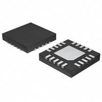
The MAX3523 is available in a 20-pin 5mm x 5mm x
0.75mm TQFN package, and operates over temperature
range of 0ºC to +70ºC.
Benefits and Features
●● Delivers +68dBmV Output Power While Meeting
DOCSIS 3.1 Requirements
●● Covers 5MHz–204MHz Output Bandwidth
●● 3.5W Power Consumption with 5V Supply Voltage
●● Programmable Power Codes Allow Operation at
Reduced Power Dissipation
●● Exceeds Spurious Requirements with Fully Loaded
OFDM Allocation at +65dBmV at Modem Output
●● 20L 5mm x 5mm x 0.75mm TQFN Package with
Exposed Paddle
Applications
●● DOCSIS 3.1 Upstream (D3.1 US)
●● Cable Modem (CM)
●● Customer Premises Equipment (CPE)
Ordering Information appears at end of data sheet.
Simplified Block Diagram
MAX3523
IN+
OUT+
IN–
OUT–
CSB
VDD
SDA
SCLK
TXEN
19-100360; Rev 0; 6/18
SERIAL INTERFACE
GND
�MAX3523
Low-Power DOCSIS 3.1
Programmable-Gain Amplifier
Absolute Maximum Ratings
VDD to GND..........................................................-0.3V to +6.0V
TXEN, SDA, SCLK, CSB......................................-0.3V to +6.0V
IN+, IN-..............................................................VDD - 2.1V to 6V
OUT+, OUT- to GND.......................................-0.3V to VDD + 5V
RF Input Power...............................................................+10dBm
Continuous Power Dissipation (TA = 70°C)
(derate 54mW/°C above TA = 70°C)..........................3500mW
Operating Junction Temperature (Note 4)......... -40°C to +150°C
Storage Temperature Range............................. -65°C to +165°C
Lead Temperature (soldering, 10s).................................. +300°C
Soldering Temperature (reflow)........................................+260°C
Stresses beyond those listed under “Absolute Maximum Ratings” may cause permanent damage to the device. These are stress ratings only, and functional operation of the device at these
or any other conditions beyond those indicated in the operational sections of the specifications is not implied. Exposure to absolute maximum rating conditions for extended periods may affect
device reliability.
Package Information
20 TQFN-EP
PACKAGE CODE
T2055+5
Outline Number
21-0140
Land Pattern Number
90-0010
Thermal Resistance, Four-Layer Board:
Junction to Ambient (θJA)
PCB must be designed for a θJA of 18.5°C/W or lower
Junction to Case (θJC)
2°C/W
For the latest package outline information and land patterns (footprints), go to www.maximintegrated.com/packages. Note that a “+”,
“#”, or “-” in the package code indicates RoHS status only. Package drawings may show a different suffix character, but the drawing
pertains to the package regardless of RoHS status.
Package thermal resistances were obtained using the method described in JEDEC specification JESD51-7, using a four-layer board.
For detailed information on package thermal considerations, refer to www.maximintegrated.com/thermal-tutorial.
www.maximintegrated.com
Maxim Integrated │ 2
�MAX3523
Low-Power DOCSIS 3.1
Programmable-Gain Amplifier
Electrical Characteristics
(VDD = 4.75V to 5.25V, VGND = 0V, ZOUT = 75Ω, TXEN = high, Gain Code = 63, Power code = 3, POUT = 68dBmV, TA = 0°C to 70°C,
Typical values are at VDD = 5V, TA = +25°C, unless otherwise noted. Typical Application Circuit as shown. Note 1.)
PARAMETER
SYMBOL
CONDITIONS
MIN
TYP
MAX
UNITS
V
DC ELECTRICAL SPECIFICATIONS
Supply Voltage
Supply Current Transmit Mode
Supply Current Transmit Disable
Mode
Input High Voltage
VDD
IDD
IDD
5.0
5.25
Gain code = 63, power code = 3
4.75
700
730
Gain code = 63, power code = 2
635
Gain code = 63, power code = 1
570
TXEN = low
2.5
VINH
2
mA
3.5
mA
VDD
V
Input Low Voltage
VINL
Input High Current
IBIASH
1
0.7
μA
V
Input Low Current
IBIASL
-1
μA
AC ELECTRICAL SPECIFICATIONS
Voltage Gain
AV
ZIN = 100Ω (Note 3),
Power Code = 3,
FIN = 10MHz
Gain code = 63
36.3
37.3
38.3
Gain code = 53
26.3
27.3
28.3
Gain code = 43
16.3
17.3
18.3
Gain code = 33
6.3
7.3
8.3
Gain code = 23
-3.7
-2.7
-1.7
Gain code = 13
-14
-13
-12
Gain code = 03
Voltage Gain Variation with Power
Code, Any Gain Code
dB
-23
∆AV
±0.1
dB
-0.5
dB
Gain Rolloff
Voltage gain = -16dB to +37dB,
fIN = 5MHz to 204MHz
Gain Step Size
Voltage gain = -16dB to +37dB,
fIN = 10MHz
Transmit-Disable Mode Noise
BW = 160kHz, 5MHz to 204MHz,
TXEN = LOW
-66
dBmV
Isolation in Transmit-Disable Mode
TXEN = LOW
80
dB
Transmit mode, voltage gain = +11dB
to +37dB
14
dB
Noise Figure Slope
Transmit mode, voltage gain = -16dB
to +37dB
-1
dB/dB
Transmit-Disable/Transmit-Enable
Transient Duration
TXEN input rise/fall time < 0.1µs
4
μs
Gain = 37dB
20
Gain = 3dB
1
Noise Figure
NF
Transmit-Disable/Transmit-Enable
Transient Amplitude
Internal Input Impedance
Output Return Loss
www.maximintegrated.com
S22
0.6
1
1.4
dB
mVpp
Differential balanced
200
Ω
5MHz - 204MHz, TXEN = high (Note 2)
13
dB
Maxim Integrated │ 3
�MAX3523
Low-Power DOCSIS 3.1
Programmable-Gain Amplifier
Electrical Characteristics (continued)
(VDD = 4.75V to 5.25V, VGND = 0V, ZOUT = 75Ω, TXEN = high, Gain Code = 63, Power code = 3, POUT = 68dBmV, TA = 0°C to 70°C,
Typical values are at VDD = 5V, TA = +25°C, unless otherwise noted. Typical Application Circuit as shown. Note 1.)
PARAMETER
SYMBOL
CONDITIONS
MIN
TYP
MAX
UNITS
Output Return Loss in TransmitDisable Mode
S22
5MHz - 204MHz, TXEN = low (Note 2)
14
dB
2nd Harmonic Distortion
HD2
fIN = 100MHz, VOUT = +68dBmV
-65
dBc
Two-Tone 2nd-Order Distortion
(f1 + f2)
IM2
f1 = 100MHz, f2 = 105MHz,
VOUT = +65dBmV/tone
-62
dBc
3rd Harmonic Distortion
HD3
fIN = 65MHz, VOUT = +68dBmV
-60
dBc
Two-Tone 3rd-Order Distortion
IM3
f1 = 195MHz, f2 = 200MHz,
VOUT = +65dBmV/tone
-55
dBc
f = 100MHz, GC = 63,
output power = +79dBmV
0.3
dB
Output Compression at Peak
Output
Modulation Error Ratio
MER
4k FFT, 1024QAM,
fIN = 150MHz,
BW = 96MHz
VOUT = +67dBmV
49
VOUT = +68dBmV
47
4k FFT, 1024QAM,
fIN = 192MHz,
BW = 24MHz
VOUT = +67dBmV
51
VOUT = +68dBmV
46
dB
CSB to SCLK Rise Setup Time
tSENS
20
ns
CSB to SCLK Rise Hold Time
tSENH
10
ns
SDA to SCLK Setup Time
tSDAS
20
ns
SDA to SCLK Hold Time
tSDAH
10
ns
SCLK Pulse-Width High
tSCLKH
50
ns
SCLK Pulse-Width Low
tSCLKL
50
ns
Maximum SCLK Frequency
fSCLK
20
MHz
Note 1: Limits are tested at TA = +70°C. Limits over the operating temperature range and relevant supply voltage range are guaranteed
by design and characterization.
Note 2: Output return loss is measured with the LC matching network, as shown in the Typical Application Circuit.
Note 3: Effective input impedance with external 200Ω resistance in parallel with internal 200Ω resistance
Note 4: The device is designed for continuous operation up to TJ = +125°C for 95,000 hours plus TJ = +150°C for 5,000 hours.
www.maximintegrated.com
Maxim Integrated │ 4
�MAX3523
Low-Power DOCSIS 3.1
Programmable-Gain Amplifier
Typical Operating Characteristics
(TA = 25°C, POUT = 68dBmV, TXEN = high, Gain Code = 63, Power Code = 3, VDD = 5V, unless otherwise noted.)
SUPPLY CURRENT
vs. GAIN CODE
800
698
500
400
300
200
100
696
695
694
VDD = 4.75V
VDD = 5.00V
VDD = 5.25V
692
0
10
20
30
40
50
60
690
70
0
15
GAIN CODE
2.4
VDD = 5.25V
37.5
37.4
45
60
37.6
37.5
PC = 2
PC = 3
0
15
30
45
60
NOISE FIGURE (dB)
20
10
0
TA = 0°C
TA = +25°C
TA = +70°C
FIN = 100MHz
18
17
16
15
13
20
30
40
GAIN CODE
www.maximintegrated.com
GC = 23
-10
GC = 13
GC = 3
0
100
50
60
70
12
0
10
20
30
40
GAIN CODE
200
300
400
500
FREQUENCY (MHz)
14
-20
toc06
GC = 33
0
-30
75
2nd HARMONIC DISTORTION
vs. FREQUENCY
toc08
19
75
GC = 43
10
-20
20
30
60
GC = 53
NOISE FIGURE
vs. GAIN CODE
toc07
45
GC = 63
TEMPERATURE (°C)
40
10
30
40
30
37.7
37.3
75
VOLTAGE GAIN
vs. GAIN CODE
0
15
VOLTAGE GAIN
vs. FREQUENCY
toc05
20
TEMPERATURE (°C)
-10
0
TEMPERATURE (°C)
37.8
37.4
30
2.3
75
VOLTAGE GAIN (dB)
VOLTAGE GAIN (dB)
VOLTAGE GAIN (dB)
37.6
15
60
PC = 0
PC = 1
37.9
37.7
0
45
38.0
VDD = 4.75V
VDD = 5.00V
VOLTAGE GAIN (dB)
30
VOLTAGE GAIN
vs. TEMPERATURE
toc04
37.8
-30
2.5
TEMPERATURE (°C)
VOLTAGE GAIN
vs. TEMPERATURE
37.3
toc03
691
50
60
-45
2nd HARMONIC DISTORTION (dBc)
0
697
693
2.6
TRANSMIT DISABLE CURRENT (mA)
699
SUPPLY CURRENT (mA)
600
TRANSMIT DISABLE CURRENT
vs. TEMPERATURE
toc02
700
PC = 3
PC = 2
PC = 1
PC = 0
700
SUPPLY CURRENT (mA)
SUPPLY CURRENT
vs. TEMPERATURE
toc01
70
POUT = +68dBmV
toc9
TA = +70°C
-50
-55
-60
-65
TA = +25°C
TA = 0°C
-70
-75
-80
0
50
100
150
200
FREQUENCY (MHz)
Maxim Integrated │ 5
�MAX3523
Low-Power DOCSIS 3.1
Programmable-Gain Amplifier
Typical Operating Characteristics (continued)
(TA = 25°C, POUT = 68dBmV, TXEN = high, Gain Code = 63, Power Code = 3, VDD = 5V, unless otherwise noted.)
-45
POUT = +68dBmV
-50
-50
-55
-55
TA = +70°C
IM2 (dBc)
-60
-65
-70
-70
TA = 0°C
TA = +25°C
-75
-80
50
100
150
200
TXEN TRANSIENT vs. GAIN CODE
0
50
10
5
30
40
50
60
-80
200
0
-25
70
TA = +70°C
0
100
54
200
300
52
52
150
200
-5
toc15
TA = 0°C
TA = +25°C
-10
-15
TA = +70°C
-20
-25
0
100
200
300
FREQUENCY (MHz)
MER vs. POUT
(OFDM, 4k FFT, 1024 QAM,
FIN = 150MHz, BW = 96MHz)
toc16
100
OUTPUT RETURN LOSS
vs. FREQUENCY
(TRANSMIT DISABLE MODE)
toc14
-15
-20
50
FREQUENCY (MHz)
FREQUENCY (MHz)
MER vs. POUT
(OFDM, 4k FFT, 1024 QAM,
FIN = 192MHz, BW = 24 MHz)
toc17
50
50
48
MER (dB)
MER (dB)
150
TA = 0°C
TA = +25°C
-10
GAIN CODE
48
46
46
44
44
42
42
40
100
-5
OUTPUT RETURN LOSS (dB)
TXEN TRANSIENT (mVp-p)
15
20
TA = 0°C
-70
OUTPUT RETURN LOSS
vs. FREQUENCY
toc13
20
10
-65
FREQUENCY (MHz)
25
0
-60
-75
FREQUENCY (MHz)
0
TA = +70°C
TA = +25°C
-55
TA = +25°C
TA = 0°C
toc12
POUT = +68dBmV
-50
-75
-80
0
-45
TA = +70°C
-60
-65
IM3 vs. FREQUENCY
toc11
POUT = +68dBmV
OUTPUT RETURN LOSS (dB)
3rd HARMONIC DISTORTION (dBc)
-45
IM2 vs. FREQUENCY
(f1 +f2)
toc10
IM3 (dBc)
3rd HARMONIC DISTORTION
vs. FREQUENCY
65
66
67
68
POUT (dBmV)
www.maximintegrated.com
69
70
40
65
66
67
68
69
70
POUT (dBmV)
Maxim Integrated │ 6
�MAX3523
Low-Power DOCSIS 3.1
Programmable-Gain Amplifier
Pin Configuration
GND
1
IN+
2
N.C.
N.C.
GND
VDD
N.C.*
TOP VIEW
20
19
18
17
16
15 N.C.
14 OUT+
EXPOSED
PADDLE
13 N.C.
GND
5
11 N.C.
6
7
8
9
10
VDD
12 OUT-
TXEN
4
CSB
N.C.
SDA
3
SCLK
IN-
NOTES:
1. CONNECT N.C. PINS TO PCB GND FOR IMPROVED HEAT DISSIPATION.
2. N.C.* PIN MUST BE LEFT UNCONNECTED.
Pin Description
PIN
NAME
10, 17
VDD
+5V Supply. Connect a 0.1μF capacitor to GND.
FUNCTION
2
IN+
Positive Input
3
IN-
Negative Input
8
CSB
Chip Select. Active-low.
7
SDA
Serial Data
6
SCLK
Clock
9
TXEN
Transmit Enable/Disable
4, 11, 13, 15,
19, 20
N.C.
Connect to PCB GND for Improved Heat Dissipation
12
OUT-
PA Negative Output
14
OUT+
PA Positive Output
1, 5, 18
GND
Ground
16
N.C.*
Leave Open
Paddle
GND
Ground
Recommended Operating Conditions
PARAMETER
CONDITIONS
Ambient Temperature Range
0°C to +70°C
www.maximintegrated.com
Maxim Integrated │ 7
�MAX3523
Low-Power DOCSIS 3.1
Programmable-Gain Amplifier
Typical Application Circuit
OUT+
MAX3523
1
T1
L2
OUTPUT
75Ω
0.01µF
R7
+
IN+
ANTI-ALIA S
FILTER
INPUT
2
12
CS
8
17
SDA
7
SCLK
6
TXEN
9
IN-
VDD_CT
C8
14
3
200Ω
C4
OUT-
VDD
0.01µF
N.C.
C2
SERIAL INTERFACE
16
N.C. N.C.
4
5
10
13
15
18
N.C.
N.C.
19
20
N.C. 11
N.C.*
L1
VDD
VDD_CT
C14
C7
R3
VDD
C5
NOTES
1. N.C. PINS TO BE LEFT OPEN OR CONNECTED TO PCB GROUND FOR IMP ROVED HE AT DISSIP ATION.
2. N.C.* PINS MUST BE LEFT UNCONNECTED.
3. FOR COMPONENT VALUES, PLEA SE RE FER TO THE MAX3523 EV KI T DATA SHEET.
Detailed Description
Programmable-Gain Amplifier
The programmable-gain amplifier (PGA) provides 60dB of
output level control in 1dB steps. The gain of the PGA is
determined by a 6-bit gain code (GC5–GC0) programmed
through the serial-data interface (see Register Map).
Specified performance is achieved when the input is
driven differentially.
Four power codes (PC1–PC0) allow the PGA to be used
with reduced bias current when distortion performance
can be relaxed. In addition, for each power code, bias current
is automatically reduced with gain code for maximum
efficiency.
The PGA features a differential Class A output stage
capable of driving an +68dBmV OFDMA signal from
5MHz–85MHz or two 96MHz +65dBmV OFDMA signals
from 5MHz–204MHz into a 75Ω load. This architecture
features a differential output that provides superior
even-order distortion performance. This requires that a
www.maximintegrated.com
transformer be used to convert to a single-ended
output. In transmit-disable mode, the output amplifiers are
powered down, resulting in low output noise while
maintaining the impedance match.
3-Wire Serial Programmable Interface (SPI)
and Control Registers
The MAX3523 includes a user-programmable register for
initializing the part and setting the gain and power
consumption. The four MSBs are address bits; the eight
least significant bits (LSBs) are used for register data.
Data is shifted MSB first.
The serial interface should only be written to when TXEN = low,
as is the case between transmit bursts in a DOCSIS
environment. Once a new set of register data is clocked
in, the corresponding power code and/or gain code does
not take effect until the 12th rising edge of SCLK.
Note: The registers must be written no earlier than 100μs after
the device is powered up.
Maxim Integrated │ 8
�MAX3523
Low-Power DOCSIS 3.1
Programmable-Gain Amplifier
SPI Read
SPI Write
Figure 1 shows a single-byte read transaction. In this
example, a single byte is read from the slave by the master.
The master first asserts CSB, begins driving SDA with the
R/Wb bit having value of 1 indicating this a read transaction
and starts toggling SCLK. The slave samples the bits on
SDA on the rising edge of SCLK. After the R/Wb bit, the
master outputs the 3-bit register addresses starting with the
most significant bit following which the master releases the
SDA line. The slave then starts driving SDA and outputs
the single byte that was requested by the master. After the
last bit has been output, the slave three-states SDA on the
rising edge of CSB that ends the transaction.
Figure 2 shows a single-byte write transaction. In this
example, a single byte is written to the slave by the
master. The master first asserts CSB, begins driving SDA
with the R/Wb bit having value of 0 indicating this a write
transaction and starts toggling SCLK. The slave samples
the bits on SDA on the rising edge of SCLK. After the R/
Wb bit, the master outputs the 3-bit register addresses
starting with the most significant bit and then the 8-bit data
starting with the most significant bit. The internal registers
are updated on the 12th rising edge of SCLK.
CSB
1
2
3
4
5
6
7
8
9
R/
Wb
A2
A1
A0
D7
D6
D5
D4
D3
SCLK
SDA
SPI MASTER DRIVES SDA
10
D2
11
D1
12
D0
MAX3523 DRIVES SDA
Figure 1. SPI Read Transaction
CSB
1
2
3
4
5
6
7
8
9
R/
Wb
A2
A1
A0
D7
D6
D5
D4
D3
SCLK
SDA
10
D2
11
D1
12
D0
SPI MASTER DRIVES SDA
Figure 2. SPI Write Transaction
www.maximintegrated.com
Maxim Integrated │ 9
�MAX3523
Low-Power DOCSIS 3.1
Programmable-Gain Amplifier
tCSS
tCSH
CSB
1
SCLK
3
2
tSDAS
A2
A1
7
6
9
8
tSCLKH
tSDAH
R/
Wb
SDA
5
4
D7
A0
10
11
12
D2
D1
D0
DATA
LATCHED
AND GAIN
CHANGES
HERE WITH R/
Wb = 0
tSCLKL
D6
D5
D4
D3
Figure 3. SPI Timing Diagram
Register Map
ADDRESS
NAME
MSB
LSB
MAIN
0x00
GAIN[7:0]
PC[1:0]
GC[5:0]
Register Details
GAIN (0x0)
BIT
7
6
5
4
3
2
Field
PC[1:0]
GC[5:0]
Reset
0x0
0x0
Write, Read
Write, Read
Access Type
BITFIELD
BITS
DESCRIPTION
0
DECODE
PC
7:6
Power Code
0x0: MIN POWER
0x3: MAX POWER
GC
5:0
Gain Code
0x0: MIN GAIN
0x3F: MAX GAIN
www.maximintegrated.com
1
Maxim Integrated │ 10
�MAX3523
Applications Information
Power Codes
The device is designed to exceed the stringent linearity
requirements of DOCSIS 3.1 using power code (PC 3).
Using lower power codes (PC = 2, 1 or 0) allows for
operation at reduced current levels. The full range of gain
codes can be used in any power code. The gain difference
between power codes is typically less than 0.1dB.
Transmit Disable Mode
Between bursts in a DOCSIS system, the MAX3523 can
be put in transmit-disable mode by setting TXEN low.
The output transient on the cable is kept well below the
DOCSIS 3.1 requirement during the TXEN transitions.
If a gain code or power code change is required, the new
values of PC and GC should be clocked in during transmitdisable mode (TXEN low). The new operating point of
the MAX3523 is set on the 12th rising edge of SCLK. This
should be done between transmission bursts.
Output Circuit
The output circuit is an open-drain differential amplifier. The
outputs should be resistively terminated, as shown in the
Typical Application Circuit. A 50:75 impedance ratio transformer
should be used as the interface between the differential output
of the device and the unbalanced 75Ω load.
Amplifier performance depends on the value of the
termination resistors. Rated performance is obtained
using the R7 termination resistor as shown in the Typical
Application Circuit. Increasing the value of this resistor will
increase gain and improve SNR at the expense of output
return loss.
Transformer core inductance may vary with temperature.
Adequate primary inductance must be present to sustain
broadband output capability as temperatures vary.
Input Circuit
The differential input impedance of the MAX3523 is
200Ω. In a typical application, however, it is driven from a
100Ω differential source, requiring an external 200Ω matching
resistor, as shown in the Typical Application Circuit.
The device has sufficient gain and linearity to produce an
output level of +68dBmV when driven with a +31dBmV input
signal. If an input level greater than +31dBmV is used, the
3rd-order distortion performance degrades.
Low-Power DOCSIS 3.1
Programmable-Gain Amplifier
Layout Issues
A well-designed printed circuit board (PCB) is an essential
part of an RF circuit. For best performance, pay attention
to power-supply layout issues as well as the output circuit
layout. The MAX3523 evaluation (EV) board layout can
be utilized as a guide during PCB design. Its electrical
performance has been thoroughly tested, making it an
excellent reference. Refer to the MAX3523 EV kit for
additional information.
Output Circuit Layout
Keep the length of the output traces as short as
possible. Series inductance between the part and the
transformer will degrade the performance at the higher
end of the operating frequency range. To maintain the
balance of the output network, match the length of the
differential traces as closely as possible.
Power-Supply Layout
For minimal coupling between different sections of the
IC, the ideal power-supply layout is a star configuration.
This configuration has a large-value decoupling capacitor at
the central power-supply node. The power-supply traces
branch out from this node, each going to a sepa
rate
power-supply node in the circuit. At the end of each of
these traces is a decoupling capacitor that provides a
very low impedance at the frequency of interest. This
arrangement provides local power-supply decoupling at
each power-supply pin. The power-supply traces must be
capable of carrying the maximum current without significant voltage drop.
Exposed Pad Thermal Considerations
The exposed pad (EP) of the MAX3523's 20-pin TQFN
package provides a low thermal resistance path to the
die. It is important that the PCB on which the device is
mounted be designed to conduct heat from this contact.
In addition, the EP should be provided with a low-induc
tance path to electrical ground. The MAX3523 EV board
is an example of a layout that provides optimal thermal
and electrical performance.
Ordering Information
PART NUMBER
TEMP RANGE
PIN-PACKAGE
MAX3523ETP+
0°C to +70°C
20 TQFN-EP*
MAX3523ETP+T
0°C to +70°C
20 TQFN-EP*
* EP = Exposed pad.
+ Denotes a lead(Pb)-free/RoHS-compliant package.
T Denotes tape-and-reel.
www.maximintegrated.com
Maxim Integrated │ 11
�MAX3523
Low-Power DOCSIS 3.1
Programmable-Gain Amplifier
Revision History
REVISION
NUMBER
REVISION
DATE
0
6/18
DESCRIPTION
Initial release
PAGES
CHANGED
—
For pricing, delivery, and ordering information, please contact Maxim Direct at 1-888-629-4642, or visit Maxim Integrated’s website at www.maximintegrated.com.
Maxim Integrated cannot assume responsibility for use of any circuitry other than circuitry entirely embodied in a Maxim Integrated product. No circuit patent licenses
are implied. Maxim Integrated reserves the right to change the circuitry and specifications without notice at any time. The parametric values (min and max limits)
shown in the Electrical Characteristics table are guaranteed. Other parametric values quoted in this data sheet are provided for guidance.
Maxim Integrated and the Maxim Integrated logo are trademarks of Maxim Integrated Products, Inc.
© 2018 Maxim Integrated Products, Inc. │ 12
�