EVALUATION KIT AVAILABLE
Click here to ask an associate for production status of specific part numbers.
MAX38640–MAX38643
Tiny 1.8V to 5.5V Input, 330nA IQ, 700mA
nanoPower Buck Converter
General Description
Benefits and Features
The MAX38640–MAX38643 are a nanoPower family of
ultra-low 330nA quiescent current buck (step-down) DCDC converters that operate from 1.8V to 5.5V input voltage and support load currents of up to 175mA, 350mA,
700mA with peak efficiencies of 96%. While in shutdown,
there is only 5nA of shutdown current. The devices offer
ultra-low quiescent current, small total solution size, and
high efficiency throughout the load range. The
MAX38640–MAX38643 are ideal for battery applications
where long battery life is a must.
● Extends Battery Life
• 330nA Ultra-Low Quiescent Supply Current
• 5nA Shutdown Current
• 96% Peak Efficiency and over 88% at 10µA
The MAX38640–MAX38643 family utilizes a unique control scheme that allows ultra-low quiescent current and
high efficiency over a wide output current range. The
MAX38642 excludes active discharge resistor in shutdown, which allows the output to be regulated or held high
by another source or by the charged output capacitor.
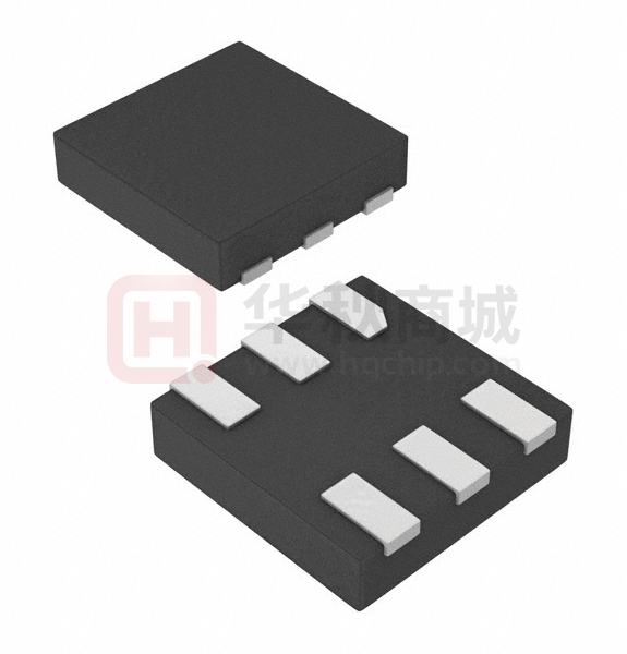
The MAX38640–MAX38643 devices are offered in a
space-saving 1.42mm x 0.89mm, 6-pin WLP (2x3 bump,
0.4mm pitch), as well as a 2mm x 2mm, 6-pin µDFN package. All parts are specified over the -40°C to +85°C extended temperature range.
● Easy to Use – Addresses Popular Operation
• 1.8V to 5.5V Input Range
• Single Resistor-Adjustable VOUT from 0.7V to 3.3V
(A-Option)
• Preprogrammed VOUT from 0.5V to 5.0V (B-Option)
• ±1.75% Output Voltage Accuracy
• Up to 175mA/350mA/700mA Load Current
● Protects System in Multiple Use Cases
• Reverse-Current Blocking in Shutdown
• Optional Active Discharge Feature
● Reduces Size and Increases Reliability
• -40°C to +85°C Temperature Range
• 2mm x 2mm, 6-pin µDFN Package
• 1.42mm x 0.89mm, 0.4mm Pitch 6-pin (2 x 3) WLP
Typical Operating Circuit
Applications
● Portable, Space-Constrained Consumer Products
● Wearable Devices, Ultra-Low-Power IoT, NB IoT, and
Bluetooth® LE
● Single Li-ion (Li+) and Coin Cell Battery Products
● Wired or Wireless Industrial Products
2.2µH
INPUT
1.8V TO 5.5V
IN
CIN
10µF
LX
OUT
OUTPUT
1.8V
COUT
22µF
MAX38640A
RSEL
EN
GND
RSEL
768kΩ
Bluetooth is a registered trademark of Bluetooth SIG, Inc.
Ordering Information appears at end of data sheet.
19-100410; Rev 10; 1/23
© 2023 Analog Devices, Inc. All rights reserved. Trademarks and registered trademarks are the property of their respective owners.
One Analog Way, Wilmington, MA 01887 U.S.A. | Tel: 781.329.4700 | © 2023 Analog Devices, Inc. All rights reserved.
�MAX38640–MAX38643
Tiny 1.8V to 5.5V Input, 330nA IQ, 700mA
nanoPower Buck Converter
TABLE OF CONTENTS
General Description . . . . . . . . . . . . . . . . . . . . . . . . . . . . . . . . . . . . . . . . . . . . . . . . . . . . . . . . . . . . . . . . . . . . . . . . . . . . . . 1
Applications . . . . . . . . . . . . . . . . . . . . . . . . . . . . . . . . . . . . . . . . . . . . . . . . . . . . . . . . . . . . . . . . . . . . . . . . . . . . . . . . . . . . 1
Benefits and Features . . . . . . . . . . . . . . . . . . . . . . . . . . . . . . . . . . . . . . . . . . . . . . . . . . . . . . . . . . . . . . . . . . . . . . . . . . . . 1
Typical Operating Circuit . . . . . . . . . . . . . . . . . . . . . . . . . . . . . . . . . . . . . . . . . . . . . . . . . . . . . . . . . . . . . . . . . . . . . . . . . 1
Absolute Maximum Ratings . . . . . . . . . . . . . . . . . . . . . . . . . . . . . . . . . . . . . . . . . . . . . . . . . . . . . . . . . . . . . . . . . . . . . . . . 5
Package Information . . . . . . . . . . . . . . . . . . . . . . . . . . . . . . . . . . . . . . . . . . . . . . . . . . . . . . . . . . . . . . . . . . . . . . . . . . . . . 5
6 µDFN . . . . . . . . . . . . . . . . . . . . . . . . . . . . . . . . . . . . . . . . . . . . . . . . . . . . . . . . . . . . . . . . . . . . . . . . . . . . . . . . . . . . . 5
6 WLP . . . . . . . . . . . . . . . . . . . . . . . . . . . . . . . . . . . . . . . . . . . . . . . . . . . . . . . . . . . . . . . . . . . . . . . . . . . . . . . . . . . . . . 5
Electrical Characteristics . . . . . . . . . . . . . . . . . . . . . . . . . . . . . . . . . . . . . . . . . . . . . . . . . . . . . . . . . . . . . . . . . . . . . . . . . 6
Typical Operating Characteristics . . . . . . . . . . . . . . . . . . . . . . . . . . . . . . . . . . . . . . . . . . . . . . . . . . . . . . . . . . . . . . . . . . 8
Pin Configurations . . . . . . . . . . . . . . . . . . . . . . . . . . . . . . . . . . . . . . . . . . . . . . . . . . . . . . . . . . . . . . . . . . . . . . . . . . . . . . 11
6 µDFN . . . . . . . . . . . . . . . . . . . . . . . . . . . . . . . . . . . . . . . . . . . . . . . . . . . . . . . . . . . . . . . . . . . . . . . . . . . . . . . . . . . . 11
6 WLP . . . . . . . . . . . . . . . . . . . . . . . . . . . . . . . . . . . . . . . . . . . . . . . . . . . . . . . . . . . . . . . . . . . . . . . . . . . . . . . . . . . . . 12
Pin Descriptions . . . . . . . . . . . . . . . . . . . . . . . . . . . . . . . . . . . . . . . . . . . . . . . . . . . . . . . . . . . . . . . . . . . . . . . . . . . . . . . 12
Functional Diagram . . . . . . . . . . . . . . . . . . . . . . . . . . . . . . . . . . . . . . . . . . . . . . . . . . . . . . . . . . . . . . . . . . . . . . . . . . . . . 13
Detailed Description . . . . . . . . . . . . . . . . . . . . . . . . . . . . . . . . . . . . . . . . . . . . . . . . . . . . . . . . . . . . . . . . . . . . . . . . . . . . 14
Voltage Configuration . . . . . . . . . . . . . . . . . . . . . . . . . . . . . . . . . . . . . . . . . . . . . . . . . . . . . . . . . . . . . . . . . . . . . . . . . 14
Applications Information . . . . . . . . . . . . . . . . . . . . . . . . . . . . . . . . . . . . . . . . . . . . . . . . . . . . . . . . . . . . . . . . . . . . . . . . . 16
Inductor Selection . . . . . . . . . . . . . . . . . . . . . . . . . . . . . . . . . . . . . . . . . . . . . . . . . . . . . . . . . . . . . . . . . . . . . . . . . . . 16
Input Capacitor . . . . . . . . . . . . . . . . . . . . . . . . . . . . . . . . . . . . . . . . . . . . . . . . . . . . . . . . . . . . . . . . . . . . . . . . . . . . . . 16
Output Capacitor . . . . . . . . . . . . . . . . . . . . . . . . . . . . . . . . . . . . . . . . . . . . . . . . . . . . . . . . . . . . . . . . . . . . . . . . . . . . 16
Enabling Device . . . . . . . . . . . . . . . . . . . . . . . . . . . . . . . . . . . . . . . . . . . . . . . . . . . . . . . . . . . . . . . . . . . . . . . . . . . . . 16
PCB Layout and Routing . . . . . . . . . . . . . . . . . . . . . . . . . . . . . . . . . . . . . . . . . . . . . . . . . . . . . . . . . . . . . . . . . . . . . . 17
Ordering Information . . . . . . . . . . . . . . . . . . . . . . . . . . . . . . . . . . . . . . . . . . . . . . . . . . . . . . . . . . . . . . . . . . . . . . . . . . . . 17
Revision History . . . . . . . . . . . . . . . . . . . . . . . . . . . . . . . . . . . . . . . . . . . . . . . . . . . . . . . . . . . . . . . . . . . . . . . . . . . . . . . 18
www.analog.com
Analog Devices | 2
�MAX38640–MAX38643
Tiny 1.8V to 5.5V Input, 330nA IQ, 700mA
nanoPower Buck Converter
LIST OF FIGURES
Figure 1. RC Circuit at EN . . . . . . . . . . . . . . . . . . . . . . . . . . . . . . . . . . . . . . . . . . . . . . . . . . . . . . . . . . . . . . . . . . . . . . . . 16
www.analog.com
Analog Devices | 3
�MAX38640–MAX38643
Tiny 1.8V to 5.5V Input, 330nA IQ, 700mA
nanoPower Buck Converter
LIST OF TABLES
Table 1. MAX38640A/1A/2A/3A RSEL Selection Table. . . . . . . . . . . . . . . . . . . . . . . . . . . . . . . . . . . . . . . . . . . . . . . . . . 14
Table 2. Inductor Selection . . . . . . . . . . . . . . . . . . . . . . . . . . . . . . . . . . . . . . . . . . . . . . . . . . . . . . . . . . . . . . . . . . . . . . . 16
www.analog.com
Analog Devices | 4
�MAX38640–MAX38643
Tiny 1.8V to 5.5V Input, 330nA IQ, 700mA
nanoPower Buck Converter
Absolute Maximum Ratings
IN, EN, RSEL, NC, OUT to GND............................... -0.3V to +6V
LX RMS Current WLP ............................. -1.6ARMS to +1.6ARMS
LX RMS Current µDFN .................................. -1ARMS to +1ARMS
LX to GND (Note 1) ........................................ -0.3V to VIN + 0.3V
Continuous Power Dissipation—WLP (TA = +70°C) (Derate
10.5mW/°C above +70°C) ................................................ 840mW
Continuous Power Dissipation—µDFN (TA = +70°C) (Derate
4.5mW/°C above +70°C) ...............................................357.8mW
Operating Temperature Range .............................-40°C to +85°C
Maximum Junction Temperature ...................................... +150°C
Storage Temperature Range ..............................-65°C to +150°C
Lead Temperature (soldering, 10 seconds) ......................+300°C
Soldering Temperature (reflow) ........................................ +260°C
Note 1: LX pin has internal clamps to GND and IN. These diodes may be forward biased during switching transitions. During these
transitions, the max LX current should be within the Max RMS Current rating for safe operation.
Stresses beyond those listed under “Absolute Maximum Ratings” may cause permanent damage to the device. These are stress ratings only, and functional operation of the
device at these or any other conditions beyond those indicated in the operational sections of the specifications is not implied. Exposure to absolute maximum rating conditions for
extended periods may affect device reliability.
Package Information
6 µDFN
Package Code
L622+1C
Outline Number
21-0164
Land Pattern Number
90-0004
Thermal Resistance, Four-Layer Board:
Junction to Ambient (θJA)
223.6°C/W
Junction to Case (θJC)
122°C/W
6 WLP
Package Code
N60E1+2
Outline Number
21-100128
Land Pattern Number
Refer to Application Note 1891
Thermal Resistance, Four-Layer Board:
Junction to Ambient (θJA)
95.15°C/W
For the latest package outline information and land patterns (footprints), go to www.maximintegrated.com/packages.
Note that a “+”, “#”, or “-” in the package code indicates RoHS status only. Package drawings may show a different
suffix character, but the drawing pertains to the package regardless of RoHS status.
Package thermal resistances were obtained using the method described in JEDEC specification JESD51-7, using a
four-layer board. For detailed information on package thermal considerations, refer to www.maximintegrated.com/
thermal-tutorial.
www.analog.com
Analog Devices | 5
�MAX38640–MAX38643
Tiny 1.8V to 5.5V Input, 330nA IQ, 700mA
nanoPower Buck Converter
Electrical Characteristics
(VIN = 3.3V, VOUT = 1.8V, TA = -40°C to +85°C, CIN = 10µF, COUT = 22µF, unless otherwise specified. (Note 2))
PARAMETER
Shutdown Current
Input Voltage Range
SYMBOL
IIN_SD
VIN_RANGE
VUVLO
Input Undervoltage
Lockout
VUVLO
Output Voltage Range
VOUT_RANGE
CONDITIONS
MIN
VEN = 0V, TA = +25°C
Guaranteed by output accuracy
TYP
MAX
UNITS
0.005
0.1
µA
5.5
V
1.8
V
1.8
RSEL > 50kΩ
(MAX38640A/1A/
2A/3A),
(MAX38640B/1B/
2B/3B)
VIN rising
1.75
Hysteresis
50
RSEL < 50kΩ
(MAX38640A/1A/
2A/3A)
VIN rising
2.6
Hysteresis
125
Guaranteed by output accuracy
-1.75
+1.75
%
VOUT = 1.8V, VIN = 2.0V to 5.5V, IOUT =
10mA to 160mA
±1.5
Quiescent Supply
Current into IN
IQ_IN
VEN = VIN, not switching VOUT = 106% of
target voltage, VOUT TARGET = 2.5V,
TA = +25°C
330
Quiescent Supply
Current into OUT
IQ_OUT
VEN = VIN, not switching VOUT = 106% of
target voltage, VOUT TARGET = 2.5V,
TA = +25°C
10
6.5
dVOUT/dt
VOUT = 1.8V, no load
LX Leakage Current
ILEAK_LX
VLX = VIN = 5.5V, TA = +25°C
Inductor Peak Current
Limit
IPEAK_LX
High-Side RDSON
Low-Side RDSON
Zero-Crossing
Threshold
Enable Input Leakage
Enable Voltage
Threshold
Active Discharge
Resistance (MAX38640/
1/3 Only)
www.analog.com
RDS_H
RDS_L
IZX_LX
ILEAK_EN
mV
V
VLREG
Soft-Start Slew Rate
%
660
mV/µs
2
100
800
1000
1200
MAX38641/MAX38642
400
500
600
MAX38640
225
250
300
MAX38643
95
150
MAX38641/
MAX38642
170
320
MAX38640
320
600
MAX38643
50
90
MAX38641/
MAX38642
80
160
MAX38640
150
290
VIN = 3.3V
VOUT = 1.2V, percent of IPEAK_LX
5
VEN = 5.5V, TA = +25°C
100
0.8
1.2
VEN rising
VEN_F
VEN falling
0.4
0.7
ROUT_DIS
VEN = 0V
50
85
nA
mA
mΩ
mΩ
%
0.1
VEN_R
nA
nA
MAX38643
VIN = 3.3V
V
5
VOUT_ACC
DC Line Regulation
2.7
0.5
OUT falling, when LX begins switching
above 1MHz, VOUT = 0.7V to 3.3V, VIN =
5.5V (Note 3)
Output Accuracy
mV
200
nA
V
Ω
Analog Devices | 6
�MAX38640–MAX38643
Tiny 1.8V to 5.5V Input, 330nA IQ, 700mA
nanoPower Buck Converter
Electrical Characteristics (continued)
(VIN = 3.3V, VOUT = 1.8V, TA = -40°C to +85°C, CIN = 10µF, COUT = 22µF, unless otherwise specified. (Note 2))
PARAMETER
SYMBOL
CONDITIONS
MIN
Required Select
Resistor Accuracy
(MAX38640A/1A/2A/3A
Only)
RSEL
Use the nearest ±1% resistor from Table
1
-1
Select Resistor
Detection Time
(MAX38640A/1A/2A/3A
Only)
tRSEL
CSEL < 2pF
Thermal Shutdown
TSHUT
TJ rising when output turns off
165
°C
Thermal Shutdown
Threshold
TSHUT
TJ falling when output turns on
150
°C
240
TYP
600
MAX
UNITS
+1
%
1320
µs
Note 2: Limits over the specified operating temperature and supply voltage range are guaranteed by design and characterization, and
production tested at room temperature only.
Note 3: Output Accuracy in low-power mode (LPM) and does not include load, line, or ripple.
www.analog.com
Analog Devices | 7
�MAX38640–MAX38643
Tiny 1.8V to 5.5V Input, 330nA IQ, 700mA
nanoPower Buck Converter
Typical Operating Characteristics
(MAX38640AENT+, VIN = 3.6V, VOUT = 1.8V, L = 2.2μH, CIN = 10μF, COUT = 22μF, TA = +25°C, unless otherwise noted.)
www.analog.com
Analog Devices | 8
�MAX38640–MAX38643
Tiny 1.8V to 5.5V Input, 330nA IQ, 700mA
nanoPower Buck Converter
Typical Operating Characteristics (continued)
(MAX38640AENT+, VIN = 3.6V, VOUT = 1.8V, L = 2.2μH, CIN = 10μF, COUT = 22μF, TA = +25°C, unless otherwise noted.)
www.analog.com
Analog Devices | 9
�MAX38640–MAX38643
Tiny 1.8V to 5.5V Input, 330nA IQ, 700mA
nanoPower Buck Converter
Typical Operating Characteristics (continued)
(MAX38640AENT+, VIN = 3.6V, VOUT = 1.8V, L = 2.2μH, CIN = 10μF, COUT = 22μF, TA = +25°C, unless otherwise noted.)
www.analog.com
Analog Devices | 10
�MAX38640–MAX38643
Tiny 1.8V to 5.5V Input, 330nA IQ, 700mA
nanoPower Buck Converter
Typical Operating Characteristics (continued)
(MAX38640AENT+, VIN = 3.6V, VOUT = 1.8V, L = 2.2μH, CIN = 10μF, COUT = 22μF, TA = +25°C, unless otherwise noted.)
Pin Configurations
6 µDFN
www.analog.com
IN
1
LX
2
GND
3
MAX3864xxELT+
6
EN
5
OUT
4
RSEL/NC
Analog Devices | 11
�MAX38640–MAX38643
Tiny 1.8V to 5.5V Input, 330nA IQ, 700mA
nanoPower Buck Converter
6 WLP
A
1
2
3
IN
LX
GND
MAX3864xxENT+
EN
B
OUT
RSEL/
NC
Pin Descriptions
PIN
MAX3864xxE
LT+
MAX3864xxE
NT+
NAME
FUNCTION
1
A1
IN
Regulator Supply Input. Connect to a voltage between 1.8V and 5.5V and bypass
with a ceramic capacitor from IN to GND.
2
A2
LX
Switching Node. Connect an inductor between LX and the regulator output.
3
A3
GND
4
B3
RSEL/NC
Ground.
MAX38640A/1A/2A/3A: Output Voltage Select Input. Connect a resistor from
RSEL to GND to program the output voltage and IN undervoltage threshold based
on Table 1.
MAX38640B/1B/2B/3B: No Connect. Leave floating.
5
B2
OUT
6
B1
EN
www.analog.com
Output Voltage Sense Input. Connect to the load at a point where accurate
regulation (output capacitor) is required to eliminate resistive metal drops.
Enable Input. Force this pin high to enable the buck converter. Force this pin low
to disable the part and enter shutdown.
Analog Devices | 12
�MAX38640–MAX38643
Tiny 1.8V to 5.5V Input, 330nA IQ, 700mA
nanoPower Buck Converter
Functional Diagram
INPUT
MAX38640A
MAX38640B
IN
REVERSE
BLOCKING
CIN
10µF
UVLO
CURRENT
SENSE
EN
MODULATOR
THERMAL
SHUTDOWN
0.6V
REFERENCE
REFERENCE
RSEL
(MAX38640A ONLY)
LX
OUT
2.2µH
OUTPUT
COUT
22µF
OPTIONAL ACTIVE
DISCHARGE
UVLO AND
TARGET OUTPUT
SELECTOR
RSEL
GND
www.analog.com
Analog Devices | 13
�MAX38640–MAX38643
Tiny 1.8V to 5.5V Input, 330nA IQ, 700mA
nanoPower Buck Converter
Detailed Description
The MAX38640–MAX38643 are ultra-low IQ (330nA) buck converters that step down from 1.8V to 5.5V to wide range of
output voltages between 0.5V and 5V. The output voltage is either programmable on the MAX38640A/1A/2A/3A versions
using an external resistor or fixed for the MAX38640B/1B/2B/3B versions. The external RSEL resistor on the RSEL pin
programs the output voltage upon startup for the MAX38640A/1A/2A/3A versions.
The buck converter automatically switches between ultra-low-power mode (ULPM), low-power mode (LPM), and highpower mode (HPM) to better service the load, depending on the load current. The buck converter overregulates in ultralow-power mode to allow the output capacitor to handle the transient load currents. The device has 90% duty cycle
limitation.
Active discharge resistor in the MAX38640/MAX38641/MAX38643 pulls OUT to ground when the part is in shutdown.
Active discharge has been strategically omitted for the MAX38642 to preserve the charge on the output capacitor in
shutdown. Harvesting applications where the output is connected to a supercapacitor can take advantage of reversecurrent blocking feature to preserve the charge on the output capacitor even if the input were to fall below the output in
shutdown. Applications where two MAX38642 buck converters are connected in parallel to drive the load can have the
input of one of the buck converters to go to 0V in shutdown without dragging the output down or loading the other buck.
Voltage Configuration
The MAX38640A/1A/2A/3A includes an RSEL pin to configure the output voltage and input UVLO threshold on startup.
Resistors with tolerance 1% (or better) should be chosen, with nominal values specified in Table 1.
Table 1. MAX38640A/1A/2A/3A RSEL Selection Table
TARGET OUTPUT VOLTAGE (V)
RSEL (kΩ)
INPUT UVLO THRESHOLD, RISING (V)
2.5
OPEN
1.75
2
909
1.75
1.8
768
1.75
1.5
634
1.75
1.3
536
1.75
1.25
452
1.75
www.analog.com
1.2
383
1.75
1.15
324
1.75
1.1
267
1.75
1.05
226
1.75
1
191
1.75
0.95
162
1.75
0.9
133
1.75
0.85
113
1.75
0.8
95.3
1.75
0.75
80.6
1.75
0.7
66.5
1.75
3.3
56.2
2.6
3
47.5
2.6
2.8
40.2
2.6
Analog Devices | 14
�MAX38640–MAX38643
Tiny 1.8V to 5.5V Input, 330nA IQ, 700mA
nanoPower Buck Converter
Table 1. MAX38640A/1A/2A/3A RSEL Selection Table (continued)
TARGET OUTPUT VOLTAGE (V)
RSEL (kΩ)
INPUT UVLO THRESHOLD, RISING (V)
2.75
34
2.6
2.5
28
2.6
2
23.7
2.6
1.8
20
2.6
1.5
16.9
2.6
1.25
14
2.6
1.2
11.8
2.6
1.15
10
2.6
1.1
8.45
2.6
1
7.15
2.6
0.95
5.9
2.6
0.9
4.99
2.6
0.8
SHORT TO GND
2.6
The MAX38640B/1B/2B/3B has a fixed output voltage that is preprogrammed (no RSEL programming). Contact Maxim
to order a part with other preprogrammed output voltage selections. The input UVLO threshold for MAX38640B/1B/2B/
3B is 1.75V (typ, VIN rising) with 50mV hysteresis (typ).
www.analog.com
Analog Devices | 15
�MAX38640–MAX38643
Tiny 1.8V to 5.5V Input, 330nA IQ, 700mA
nanoPower Buck Converter
Applications Information
Inductor Selection
The inductor value for the MAX38640–MAX38643 affects the ripple current, the transition point from low-power mode
(LPM) to ultra-low-power mode (ULPM), and the overall efficiency performance. Based on the peak current limit required
for different applications, it is recommended to select an inductor value based on Table 2.
Table 2. Inductor Selection
PEAK CURRENT, PART NUMBER
INDUCTANCE RANGE (µH)
1.0A, MAX38643
1.0 to 1.5
500mA, MAX38641/MAX38642
2.2
250mA, MAX38640
2.2 to 4.7
Input Capacitor
The input capacitor (CIN) reduces the peak current drawn from the battery or input power source and reduces the
switching noise in the IC. The impedance of CIN at the switching frequency should be very low. Ceramic capacitors are
recommended with their small size and low ESR. For most MAX38640 applications, use a 10µF ceramic capacitor with
X5R or X7R temperature characteristics.
For MAX38641–MAX38643 applications, using a 22µF ceramic input capacitor is recommended. When operating at VIN
close to the UVLO, more input capacitance may be required to keep the input voltage ripple from tripping the UVLO
protection.
Output Capacitor
The output capacitor (COUT) is required to keep the output voltage ripple small and to ensure loop stability. COUT must
have low impedance at the switching frequency. Ceramic capacitors are recommended due to their small size and low
ESR. Make sure the capacitor does not degrade its capacitance significantly over temperature and DC bias. Capacitors
with X5R or X7R temperature characteristics typically perform well. A 22µF ceramic capacitor is recommended for most
MAX38640 and MAX38641/MAX38642 applications. In case of low VOUT target levels when using the MAX38641/
MAX38642, two 22µF output capacitors are recommended. For MAX38643 applications, use two 22µF output capacitors.
Enabling Device
The device has a dedicated EN pin. This pin can be driven by a digital signal. It is recommended that the digital signal
enables the device after VIN crosses the UVLO threshold. In applications where EN is tied to IN, the device is designed
to be powered by fast VIN slew rates. If VIN slew rates are slower than 5V/ms, users must delay enabling the device until
after VIN crosses the UVLO threshold. This can be done using a simple RC circuit, as shown in Figure 1.
IN
BAT54
REN
EN
CEN
Figure 1. RC Circuit at EN
www.analog.com
Analog Devices | 16
�MAX38640–MAX38643
Tiny 1.8V to 5.5V Input, 330nA IQ, 700mA
nanoPower Buck Converter
PCB Layout and Routing
High switching frequencies and large peak currents make PCB layout a very important part of the buck regulator design.
Good design minimizes excessive electromagnetic interference (EMI) on the feedback paths and voltage gradients in the
ground plane to avoid instability and regulation errors. The input capacitor (CIN) should be placed as close as possible
to the IC pins IN and GND. Connect the inductor, CIN, and output capacitor (COUT) as close together as possible, and
keep their traces short, direct, and wide.
Connect the two GND pins under the IC and directly to the ground of COUT. Keep noisy traces, such as the LX node, as
short as possible. The OUT pin should be connected to the output capacitor and this trace should be routed away from
the main power path between the inductor and COUT. The OUT trace should also be routed away from noisy traces such
as the LX line or other external noise sources. Refer to the MAX38640–MAX38643 evaluation kit for an example PCB
layout and routing scheme.
Ordering Information
OUTPUT
CURRENT
(mA)
ACTIVE
DISCHARGE
MAX38640AELT+
175
Yes
MAX38641AELT+
350
Yes
MAX38642AELT+
350
No
MAX38643AELT+
700
Yes
MAX38640BELT+*
175
Yes
MAX38641BELT+*
350
Yes
MAX38642BELT+*
350
No
MAX38643BELT+*
700
Yes
MAX38640BELT18+T
175
Yes
1.8V Preprogrammed Output Voltage
MAX38640BELT21+T
175
Yes
2.1V Preprogrammed Output Voltage
MAX38640AENT+
175
Yes
MAX38641AENT+
350
Yes
MAX38642AENT+
350
No
MAX38643AENT+
700
Yes
MAX38640BENT+*
175
Yes
MAX38642BENT+*
350
No
MAX38643BENT+*
700
Yes
MAX38641BENT135+
350
Yes
1.35V Preprogrammed Output Voltage
MAX38640BENT06+T
175
Yes
0.6V Preprogrammed Output Voltage
MAX38640BENT065+T
175
Yes
0.65V Preprogrammed Output Voltage
MAX38640BENT21+T
175
Yes
2.1V Preprogrammed Output Voltage
MAX38643BENT185+T
700
Yes
1.85V Preprogrammed Output Voltage
MAX38641BENT12+T
350
Yes
1.2V Preprogrammed Output Voltage
MAX38640BENT18+T
175
Yes
1.8V Preprogrammed Output Voltage
PART NUMBER
FEATURES
PACKAGE
0.7V to 3.3V Resistor-Selectable Output Voltage
Using RSEL Pin
0.5V to 5V Preprogrammed Output Voltage
6-pin, 2mm x 2mm
μDFN
0.7V to 3.3V Resistor-Selectable Output Voltage
Using RSEL Pin
0.5V to 5V Preprogrammed Output Voltage
0.4mm pitch, 6-pin
(2x3) WLP
*Future product—contact factory for availability.
+Denotes a lead(Pb)-free/RoHS-compliant package.
T = Tape and reel.
www.analog.com
Analog Devices | 17
�MAX38640–MAX38643
Tiny 1.8V to 5.5V Input, 330nA IQ, 700mA
nanoPower Buck Converter
Revision History
REVISION
NUMBER
REVISION
DATE
0
10/18
Initial release
1
1/19
Updated Typical Operating Characteristics, Pin Descriptions, Functional Diagram,
Applications Information, and Ordering Information
5, 6, 8, 9, 13, 14
2
5/19
Updated title of data sheet and changed part number references, updated Typical
Operating Characteristics
1, 3–5, 7, 9–15
3
4/20
Updated Ordering Information
4
9/20
Updated Ordering Information
5
3/21
Removed Table 2, updated Ordering Information
6
8/21
Updated Absolute Maximum Ratings, Electrical Characteristics, Functional Diagram,
and Ordering Information
7
1/22
Updated Ordering Information
14
8
2/22
Updated Ordering Information
14
9
4/22
Updated Typical Operating Characteristics
10
10
1/23
Updated Ordering Information
17
DESCRIPTION
PAGES
CHANGED
—
14
14
12, 14
2, 3, 10, 14
Information furnished by Analog Devices is believed to be accurate and reliable. However, no responsibility is
assumed by Analog Devices for its use, nor for any infringements of patents or other rights of third parties that may
result from its use. Specifications subject to change without notice. No license is granted by implication or otherwise
under any patent or patent rights of Analog Devices. Trademarks and registered trademarks are the property of
their respective owners.
w w w . a n a l o g . c o m
Analog Devices | 18
�