19-2726; Rev 3; 12/03
3.3V, 16-Bit, 500Msps High Dynamic
Performance DAC with Differential LVDS Inputs
♦ Single 3.3V Supply Operation
♦ Excellent SFDR and IMD Performance
SFDR = 76dBc at fOUT = 40MHz (to Nyquist)
IMD = -85dBc at fOUT = 10MHz
ACLR = 73dB at fOUT = 61MHz
♦ 2mA to 20mA Full-Scale Output Current
♦ Differential, LVDS-Compatible Digital and Clock
Inputs
♦ On-Chip 1.2V Bandgap Reference
♦ Low 130mW Power Dissipation
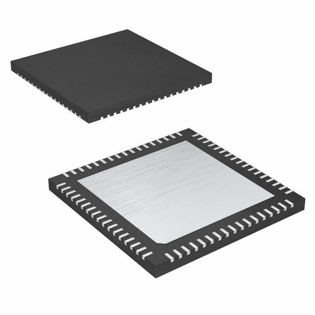
♦ 68-Lead QFN-EP Package
Ordering Information
PART
MAX5888AEGK
-40°C to +85°C
68 QFN-EP*
MAX5888EGK
-40°C to +85°C
68 QFN-EP*
*EP = Exposed paddle.
68
Applications
Communications: LMDS, MMDS, Point-to-Point
Microwave
Digital Signal Synthesis
Automated Test Equipment (ATE)
Instrumentation
63 62 61 60 59 58
B10N
B10P
B9P
B9N
B8P
B8N
B7P
B7N
DGND
DVDD
DGND
B6N
67 66 65 64
B6P
B5P
B5N
Pin Configuration
TOP VIEW
Base Stations: Single-/Multicarrier UMTS,
CDMA, GSM
PINPACKAGE
TEMP RANGE
B4P
The digital and clock inputs of the MAX5888 are
designed for differential low-voltage differential signal
(LVDS)-compatible voltage levels. The MAX5888 is
available in a 68-lead QFN package with an exposed
paddle (EP) and is specified for the extended industrial
temperature range (-40°C to +85°C).
Refer to the MAX5887 and MAX5886 data sheets for
pin-compatible 14- and 12-bit versions of the MAX5888.
♦ 500Msps Output Update Rate
B4N
The MAX5888 utilizes a current-steering architecture,
which supports a full-scale output current range of 2mA
to 20mA, and allows a differential output voltage swing
between 0.1VP-P and 1VP-P.
The MAX5888 features an integrated 1.2V bandgap reference and control amplifier to ensure high accuracy
and low noise performance. Additionally, a separate
reference input pin enables the user to apply an external reference source for optimum flexibility and to
improve gain accuracy.
Features
57 56 55 54 53 52
EP
B3P
1
B3N
2
50 B11P
B2P
3
49 B12N
B2N
4
48 B12P
B1P
5
47 B13N
B1N
6
46 B13P
B0P
7
45 B14N
B0N
8
DGND
9
51 B11N
44 B14P
MAX5888
43 B15N
DVDD 10
42 B15P
VCLK 11
41 DGND
CLKGND 12
40 DVDD
CLKP 13
39 SEL0
CLKN 14
38 N.C.
CLKGND 15
37 N.C.
VCLK 16
36 N.C.
PD 17
35 N.C.
N.C.
AGND
AVDD
AGND
AVDD
AVDD
AGND
IOUTP
IOUTN
AVDD
AGND
N.C.
DACREF
FSADJ
REFIO
AVDD
AGND
18 19 20 21 22 23 24 25 26 27 28 29 30 31 32 33 34
QFN
________________________________________________________________ Maxim Integrated Products
For pricing, delivery, and ordering information, please contact Maxim/Dallas Direct! at
1-888-629-4642, or visit Maxim’s website at www.maxim-ic.com.
1
MAX5888
General Description
The MAX5888 is an advanced, 16-bit, 500Msps digitalto-analog converter (DAC) designed to meet the
demanding performance requirements of signal synthesis applications found in wireless base stations and
other communications applications. Operating from a
single 3.3V supply, this DAC offers exceptional dynamic performance such as 76dBc spurious-free dynamic
range (SFDR) at fOUT = 40MHz. The DAC supports
update rates of 500Msps and a power dissipation of
only 250mW.
�MAX5888
3.3V, 16-Bit, 500Msps High Dynamic
Performance DAC with Differential LVDS Inputs
ABSOLUTE MAXIMUM RATINGS
Continuous Power Dissipation (TA = +70°C)
68-Lead QFN-EP (derate 41.7mW/°C above +70°C) ...3333mW
Thermal Resistance (θJA) ..............................................+24°C/W
Operating Temperature Range ..........................-40°C to +85°C
Junction Temperature .....................................................+150°C
Storage Temperature Range ............................-60°C to +150°C
Lead Temperature (soldering, 10s) ................................+300°C
AVDD, DVDD, VCLK to AGND................................-0.3V to +3.9V
AVDD, DVDD, VCLK to DGND ...............................-0.3V to +3.9V
AVDD, DVDD, VCLK to CLKGND ...........................-0.3V to +3.9V
AGND, CLKGND to DGND....................................-0.3V to +0.3V
DACREF, REFIO, FSADJ to AGND.............-0.3V to AVDD + 0.3V
IOUTP, IOUTN to AGND................................-1V to AVDD + 0.3V
CLKP, CLKN to CLKGND...........................-0.3V to VCLK + 0.3V
B0P/B0N–B15P/B15N, SEL0,
PD to DGND ...........................................-0.3V to DVDD + 0.3V
Stresses beyond those listed under “Absolute Maximum Ratings” may cause permanent damage to the device. These are stress ratings only, and functional
operation of the device at these or any other conditions beyond those indicated in the operational sections of the specifications is not implied. Exposure to
absolute maximum rating conditions for extended periods may affect device reliability.
ELECTRICAL CHARACTERISTICS
(AVDD = DVDD = VCLK = 3.3V, AGND = DGND = CLKGND = 0, external reference, VREFIO = 1.25V, differential transformer-coupled
analog output, 50Ω double terminated (Figure 7), IOUT = 20mA, TA = TMIN to TMAX, unless otherwise noted. ≥+25°C guaranteed by
production test, 45dB for the first adjacent carrier slot
(ACLR 1) and >50dB for the second adjacent carrier
slot (ACLR 2). This specification applies to the output of
the entire transmitter signal chain. The requirement for
only the DAC block of the transmitter must be tighter,
with a typical margin of >15dB, requiring the DAC’s
ACLR 1 to be better than 60dB. Adjacent channel leakage is caused by a single-spread spectrum carrier,
which generates intermodulation (IM) products
between the frequency components located within the
carrier band. The energy at one end of the carrier band
generates IM products with the energy from the opposite end of the carrier band. For single-carrier WCDMA
modulation, these IMD products are spread 3.84MHz
over the adjacent sideband. Four contiguous WCDMA
______________________________________________________________________________________
�3.3V, 16-Bit, 500Msps High Dynamic
Performance DAC with Differential LVDS Inputs
-25
-30
-40
The transmitter sections of multicarrier base station
transceiver systems for GSM/EDGE usually present
communication DAC manufacturers with the difficult
task of providing devices with higher resolution, while
simultaneously reducing noise and spurious emissions
over a desired bandwidth.
To specify noise and spurious emissions from base stations, a GSM/EDGE Tx mask is used to identify the DAC
requirements for these parameters. This mask shows
that the allowable levels for noise and spurious emissions are dependent on the offset frequency from the
transmitted carrier frequency. The GSM/EDGE mask
and its specifications are based on a single active carrier with any other carriers in the transmitter being disabled. Specifications displayed in Figure 11 support
per-carrier output power levels of 20W or greater.
Lower output power levels yield less stringent emission
requirements. For GSM/EDGE applications, the DAC
demands spurious emission levels of less than -80dBc
for offset frequencies ≥6MHz. Spurious products from
the DAC can combine with both random noise and spurious products from other circuit elements. The spurious products from the DAC should therefore be backed
off by 6dB more to allow for these other sources and
still avoid signal clipping.
-30
fCENTER = 61.44MHz
fCLK = 184.32Mbps
ACLR = 73dB
-40
-50
OUTPUT POWER (dBm)
-50
OUTPUT POWER (dBm)
Multitone Testing for GSM/EDGE
Applications
-60
-70
-80
-90
-100
-60
-70
-80
-90
-100
-110
-110
-120
-120
-125
fCENTER = 61.44MHz
fCLK = 184.32Mbps
ACLR = 65dB
-130
3.5MHz/div
Figure 9. ACLR for WCDMA Modulation, Single Carrier
3.5MHz/div
Figure 10. ACLR for WCDMA Modulation, Four Carriers
*Note that due to their own IM effects and noise limitations, spectrum analyzers introduce ACLR errors, which can falsify the measurement. For a single-carrier ACLR measurement greater than 70dB, these measurement limitations are significant, becoming even more
restricting for multicarrier measurement. Before attempting an ACLR measurement, it is recommended consulting application notes provided by major spectrum analyzer manufacturers that provide useful tips on how to use their instruments for such tests.
______________________________________________________________________________________
13
MAX5888
carriers spread their IM products over a bandwidth of
20MHz on either side of the 20MHz total carrier bandwidth. In this four-carrier scenario, only the energy in
the first adjacent 3.84MHz side band is considered for
ACLR 1. To measure ACLR, drive the converter with a
WCDMA pattern. Make sure that the signal is backed
off by the peak-to-average ratio, such that the DAC is
not clipping the signal. ACLR can then be measured
with the ACLR measurement function built into your
spectrum analyzer.
Figure 9 shows the ACLR performance for a single
WCDMA carrier (fCLK = 184.32MHz, fOUT = 61.44MHz)
applied to the MAX5888 (including measurement system limitations*).
Figure 10 illustrates the ACLR test results for the
MAX5888 with a four-carrier WCDMA signal at an output frequency of 61.44MHz and sampling frequency of
184.32MHz. Again, the noise floor of the instrument
restricts the signal’s real dynamic range of the signal,
and the measured ACLR 1 understates the actual by
more than 2.5dB. Considerable care must be taken to
ensure accurate measurement of this parameter.
�MAX5888
3.3V, 16-Bit, 500Msps High Dynamic
Performance DAC with Differential LVDS Inputs
The number of carriers and their signal levels with
respect to the full scale of the DAC are important as
well. Unlike a full-scale sine wave, the inherent nature of
a multitone signal contains higher peak-to-RMS ratios,
raising the prospect for potential clipping, if the signal
level is not backed off appropriately. If a transmitter
operates with four/eight in-band carriers, each individual carrier must be operated at less than
-12dB FS/-18dB FS to avoid waveform clipping.
The noise density requirements (Table 2) for a
GSM/EDGE-based system can again be derived from
the system’s Tx mask. With a worst-case noise level of
-80dBc at frequency offsets of ≥6MHz and a measurement bandwidth of 100kHz, the minimum noise density
per hertz is calculated as follows:
SNRMIN = -80dBc - 10 ✕ log10(100 ✕ 103Hz)
SNRMIN = -130dBc/Hz
Since random DAC noise adds to both the spurious tones
and to random noise from other circuit elements, it is recommended reducing the specification limits by about
10dB to allow for these additional noise contributions
while maintaining compliance with the Tx mask values.
Other key factors in selecting the appropriate DAC for
the Tx path of a multicarrier GSM/EDGE system is the
converter’s ability to offer superior IMD and MTPR performance. Multiple carriers in a designated band generate
unwanted intermodulation distortion between the individual carrier frequencies. A multitone test vector usually
consists of several equally spaced carriers, usually four,
with identical amplitudes. Each of these carriers is representative of a channel within the defined bandwidth of
interest. To verify MTPR, one or more tones are
removed such that the intermodulation distortion perfor-
Table 2. GSM/EDGE Noise Requirements
for Multicarrier Systems
NUMBER OF
CARRIERS
CARRIER
POWER LEVEL
(dB FS)
DAC NOISE DENSITY
REQUIREMENT
(dB FS/Hz)
2
-6
-146
4
-12
-152
8
-18
-158
mance of the DAC can be evaluated. Nonlinearities
associated with the DAC create spurious tones, some
of which may fall back into the area of the removed
tone, limiting a channel’s carrier-to-noise ratio. Other
spurious components falling outside the band of interest can also be important, depending on the system’s
spectral mask and filtering requirements. Going back to
the GSM/EDGE Tx mask, the IMD specification for adjacent carriers varies somewhat among the different GSM
standards. For the PCS1800 and GSM850 standards,
the DAC must meet an average IMD of -70dBc.
Table 3 summarizes the dynamic performance requirements for the entire Tx signal chain in a four-carrier
GSM/EDGE-based system and compares the previously established converter requirements with a new-generation high dynamic performance DAC.
The four-tone MTPR plot in Figure 12 demonstrates the
MAX5888’s excellent dynamic performance. The center
frequency (fCENTER = 31.97MHz) has been removed to
allow detection and analysis of intermodulation or spurious components falling back into this empty spot from
adjacent channels. The four carriers are observed over
a 12MHz bandwidth and are equally spaced at 1MHz.
Each individual output amplitude is backed off to -12dB
FS. Under these conditions, the DAC yields an MTPR
performance of -78dBc.
Table 3. Summary of Important AC Performance Parameters for Multicarrier GSM/EDGE
Systems
SPECIFICATION
SYSTEM TRANSMITTER
OUTPUT LEVELS
DAC REQUIREMENTS WITH
MARGINS
MAX5888 SPECIFICATIONS
SFDR
80dBc
86dBc
82dBc*
SNR
-130dBc/Hz
-152dB FS/Hz
-165dB/Hz
IMD
-70dBc
-75dBc
-78dBc
N/S
-12dB FS
-12dB FS
Carrier Amplitude
*Measured within a 25MHz window.
14
______________________________________________________________________________________
�3.3V, 16-Bit, 500Msps High Dynamic
Performance DAC with Differential LVDS Inputs
MAX5888
4-TONE MULTITONE POWER RATIO PLOT
(fCLK = 300MHz, fCENTER = 31.9702MHz)
0
AOUT = -12dB FS
BW = 12MHz
-10
INBAND
30kHz 100kHz
-60
-20
4-TONE MTPR (dBm)
MEASUREMENT BANDWIDTH
-30
OUTBAND
TRANSMITTER EDGE
AMPLITUDE (dBc)
O
fT3
fT1
-30
fT4
fT2
-40
-50
-60
-70
IMD REQUIREMENT: < -70dBc
-70
-73
-75
-80
-80
WORST-CASE
NOISE LEVEL
-90
-90
-100
26
0.2 0.4 0.6
1.2
1.8
28
30
6.0
FREQUENCY OFFSET FROM CARRIER (MHz)
Figure 11. GSM/EDGE Tx Mask
Grounding, Bypassing, and Power-Supply
Considerations
Grounding and power-supply decoupling can strongly
influence the performance of the MAX5888. Unwanted
digital crosstalk may couple through the input, reference, power supply, and ground connections, affecting
dynamic performance. Proper grounding and powersupply decoupling guidelines for high-speed, high-frequency applications should be closely followed. This
reduces EMI and internal crosstalk that can significantly affect the dynamic performance of the MAX5888.
Use of a multilayer printed circuit (PC) board with separate ground and power-supply planes is recommended. High-speed signals should run on lines directly
above the ground plane. Since the MAX5888 has separate analog and digital ground buses (AGND,
CLKGND, and DGND, respectively), the PC board
should also have separate analog and digital ground
sections with only one point connecting the two planes.
Digital signals should be run above the digital ground
plane and analog/clock signals above the analog/clock
ground plane. Digital signals should be kept as far
away from sensitive analog inputs, reference inputs
sense lines, common-mode input, and clock inputs as
fT1 = 30.0659MHz
fT2 = 31.0181MHz
fT3 = 33.0688MHz
fT4 = 34.0209MHz
32
34
36
38
fOUT (MHz)
Figure 12. 4-Tone MTPR Test Results, fCENTER = 31.97MHz,
fCLK = 300MHz
practical. A symmetric design of clock input and analog output lines is recommended to minimize 2nd-order
harmonic distortion components and optimize the
DAC’s dynamic performance. Digital signal paths
should be kept short and run lengths matched to avoid
propagation delay and data skew mismatches.
The MAX5888 supports three separate power-supply
inputs for analog (AVDD), digital (DVDD), and clock
(VCLK) circuitry. Each AVDD, DVDD, and VCLK input
should at least be decoupled with a separate 0.1µF
capacitor as close to the pin as possible and their
opposite ends with the shortest possible connection to
the corresponding ground plane (Figure 13). Try to
minimize the analog and digital load capacitances for
optimized operation. All three power-supply voltages
should also be decoupled at the point they enter the
PC board with tantalum or electrolytic capacitors.
Ferrite beads with additional decoupling capacitors
forming a pi network could also improve performance.
The analog and digital power-supply inputs AV DD ,
VCLK, and DVDD of the MAX5888 allow a supply voltage range of 3.3V ±5%.
______________________________________________________________________________________
15
�MAX5888
3.3V, 16-Bit, 500Msps High Dynamic
Performance DAC with Differential LVDS Inputs
DAC. An array of at least 4 ✕ 4 vias (≤0.3mm diameter
per via hole and 1.2mm pitch between via holes) is recommended for this 68-lead QFN-EP package.
The MAX5888 is packaged in a 68-lead QFN-EP
package (package code: G6800-4), providing greater
design flexibility, increased thermal efficiency**, and
optimized AC performance of the DAC. The exposed
pad (EP) enables the user to implement grounding
techniques, which are necessary to ensure highest performance operation. The EP must be soldered down
to AGND.
In this package, the data converter die is attached to
an EP lead frame with the back of this frame exposed at
the package bottom surface, facing the PC board side
of the package. This allows a solid attachment of the
package to the PC board with standard infrared (IR)
flow soldering techniques. A specially created land pattern on the PC board, matching the size of the EP (6mm
✕ 6mm), ensures the proper attachment and grounding
of the DAC. Designing vias*** into the land area and
implementing large ground planes in the PC board
design allow for highest performance operation of the
Static Performance Parameter Definitions
Integral Nonlinearity (INL)
Integral nonlinearity is the deviation of the values on an
actual transfer function from either a best straight line fit
(closest approximation to the actual transfer curve) or a
line drawn between the end points of the transfer function, once offset and gain errors have been nullified. For
a DAC, the deviations are measured at every individual
step.
Differential Nonlinearity (DNL)
Differential nonlinearity is the difference between an
actual step height and the ideal value of 1 LSB. A DNL
error specification of less than 1 LSB guarantees no
missing codes and a monotonic transfer function.
**Thermal efficiency is not the key factor, since the MAX5888 features low-power operation. The exposed pad is the key element to
ensure a solid ground connection between the DAC and the PC board’s analog ground layer.
***Vias connect the land pattern to internal or external copper planes. It is important to connect as many vias as possible to the analog
ground plane to minimize inductance.
BYPASSING—DAC LEVEL
BYPASSING—BOARD LEVEL
AVDD
AVDD
VCLK
FERRITE BEAD
1µF
0.1µF
0.1µF
AGND
10µF
47µF
ANALOG POWERSUPPLY SOURCE
47µF
DIGITAL POWERSUPPLY SOURCE
47µF
CLOCK POWERSUPPLY SOURCE
CLKGND
DVDD
OUTP
B0–B15
FERRITE BEAD
MAX5888
1µF
16
10µF
OUTN
0.1µF
VCLK
FERRITE BEAD
DGND
1µF
DVDD
10µF
Figure 13. Recommended Power-Supply Decoupling and Bypassing Circuitry
16
______________________________________________________________________________________
�3.3V, 16-Bit, 500Msps High Dynamic
Performance DAC with Differential LVDS Inputs
Gain Error
A gain error is the difference between the ideal and the
actual full-scale output voltage on the transfer curve,
after nullifying the offset error. This error alters the slope
of the transfer function and corresponds to the same
percentage error in each step.
Settling Time
The settling time is the amount of time required from the
start of a transition until the DAC output settles its new
output value to within the converter’s specified accuracy.
Glitch Energy
Glitch impulses are caused by asymmetrical switching
times in the DAC architecture, which generates undesired output transients. The amount of energy that
appears at the DAC’s output is measured over time and
usually specified in the pV-s range.
Dynamic Performance Parameter
Definitions
Signal-to-Noise Ratio (SNR)
For a waveform perfectly reconstructed from digital samples, the theoretical maximum SNR is the ratio of the fullscale analog output (RMS value) to the RMS quantization
error (residual error). The ideal, theoretical minimum can
be derived from the DAC’s resolution (N bits):
SNRdB = 6.02dB ✕ N + 1.76dB
Spurious-Free Dynamic Range (SFDR)
SFDR is the ratio of RMS amplitude of the carrier frequency (maximum signal components) to the RMS
value of their next-largest distortion component. SFDR
is usually measured in dBc and with respect to the carrier frequency amplitude or in dB FS with respect to the
DAC’s full-scale range. Depending on its test condition,
SFDR is observed within a predefined window or
to Nyquist.
Two-/Four-Tone Intermodulation
Distortion (IMD)
The two-tone IMD is the ratio expressed in dBc (or dB
FS) of either input tone to the worst 3rd-order (or higher) IMD products. Note that 2nd-order IMD products
usually fall at frequencies that can be easily removed
by digital filtering; therefore, they are not as critical as
3rd-order IMDs. The two-tone IMD performance of the
MAX5888 was tested with the two individual input tone
levels set to at least -6dB FS and the four-tone performance was tested according to the GSM model at an
output frequency of 32MHz and amplitude of -12dB FS.
Adjacent Channel Leakage
Power Ratio (ACLR)
Commonly used in combination with WCDMA, ACLR
reflects the leakage power ratio in dB between the
measured power within a channel relative to its adjacent channel. ACLR provides a quantifiable method of
determining out-of-band spectral energy and its influence on an adjacent channel when a bandwidth-limited
RF signal passes through a nonlinear device.
Chip Information
TRANSISTOR COUNT: 10,629
PROCESS: CMOS
However, noise sources such as thermal noise, reference noise, clock jitter, etc., affect the ideal reading;
therefore, SNR is computed by taking the ratio of the
RMS signal to the RMS noise, which includes all spectral components minus the fundamental, the first four
harmonics, and the DC offset.
______________________________________________________________________________________
17
MAX5888
Offset Error
The offset error is the difference between the ideal and
the actual offset current. For a DAC, the offset point is
the value at the output for the two midscale digital input
codes with respect to the full scale of the DAC. This
error affects all codes by the same amount.
�Package Information
(The package drawing(s) in this data sheet may not reflect the most current specifications. For the latest package outline information,
go to www.maxim-ic.com/packages.)
68L QFN.EPS
MAX5888
3.3V, 16-Bit, 500Msps High Dynamic
Performance DAC with Differential LVDS Inputs
PACKAGE OUTLINE, 68L QFN, 10x10x0.9 MM
1
C
21-0122
2
*
*MAX5888 Package Code
PACKAGE OUTLINE, 68L QFN, 10x10x0.9 MM
1
C
21-0122
2
Maxim cannot assume responsibility for use of any circuitry other than circuitry entirely embodied in a Maxim product. No circuit patent licenses are
implied. Maxim reserves the right to change the circuitry and specifications without notice at any time.
18 ____________________Maxim Integrated Products, 120 San Gabriel Drive, Sunnyvale, CA 94086 408-737-7600
© 2003 Maxim Integrated Products
Printed USA
is a registered trademark of Maxim Integrated Products.
�