19-4806; Rev 1; 4/10
KIT
ATION
EVALU
E
L
B
AVAILA
Mono 2W Class D Amplifier
Features
The MAX9830 mono 2W Class D amplifier provides
Class AB audio performance with Class D efficiency.
o Industry-Leading Quiescent Current: 1.6mA at 5V,
1.2mA at 3.6V
Active emissions limiting edge rate and overshoot control circuitry greatly reduces EMI. A filterless spreadspectrum modulation scheme eliminates the need for
output filtering found in traditional Class D devices.
These features reduce application component count.
The MAX9830’s industry-leading 1.6mA at 5V, 1.2mA at
3.6V, quiescent current extends battery life in portable
applications.
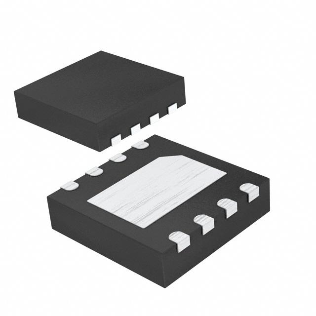
The MAX9830 is available in an 8-pin TDFN (2mm x
2mm x 0.8mm) and is specified over the extended
-40°C to +85°C temperature range.
o Spread Spectrum and Active Emissions Limiting
o Passes EMI Limit Unfiltered with Up to 24in
(61cm) of Speaker Cable
o Click-and-Pop Suppression
o Thermal and Overcurrent Protection
o Low 0.5μA Current Shutdown Mode
o Space-Saving, 2mm x 2mm x 0.8mm, 8-Pin TDFN
Package
Applications
Ordering Information
Notebook and Netbook Computers
Cellular Phones
PART
MP3 Players
MAX9830AETA+
TEMP RANGE
PIN-PACKAGE
-40°C to +85°C
8 TDFN-EP*
Portable Audio Players
+Denotes a lead(Pb)-free/RoHS-compliant package.
VoIP Phones
*EP = Exposed pad.
Typical Operating Circuit
Pin Configuration
TOP VIEW
PVDD OUT+ OUT- PGND
8
7
6
5
+2.6V TO +5.5V
0.47μF
IN+
PVDD
0.1μF
0.47μF
MAX9830
IN-
MAX9830
OUT+
*EP
+
SHDN
OUT-
1
2
IN+
IN-
3
4
SHDN N.C.
N.C.
PGND
TDFN
2mm x 2mm x 0.8mm
*EP = EXPOSED PAD. CONNECT THE EP TO
PGND TO ENHANCE THERMAL DISSIPATION.
________________________________________________________________ Maxim Integrated Products
For pricing, delivery, and ordering information, please contact Maxim Direct at 1-888-629-4642,
or visit Maxim’s website at www.maxim-ic.com.
1
MAX9830
General Description
�MAX9830
Mono 2W Class D Amplifier
ABSOLUTE MAXIMUM RATINGS
Voltage
PVDD, IN+, IN-, SHDN, to PGND .........................-0.3V to +6V
OUT+, OUT- to PGND...........................-0.3V to VPVDD + 0.3V
Current
Continuous Current Into/Out of PVDD, PGND,
OUT+, OUT- ..............................................................±600mA
Continuous Input Current (all other pins) .....................±20mA
Duration of Short Circuit Between
OUT+, OUT-, and PVDD, PGND ............................Continuous
Continuous Power Dissipation for a Multilayer Board
(TA = +70°C)
8-Pin TDFN-EP (derate 11.9mW/°C) .........................953.5mW
Junction Temperature ......................................................+150°C
Operating Temperature Range ...........................-40°C to +85°C
Storage Temperature Range .............................-65°C to +150°C
Lead Temperature (soldering, 10s) .................................+300°C
Soldering Temperature (reflow) .......................................+260°C
Rate of Voltage Rise at PVDD .............................................1V/μs
Stresses beyond those listed under “Absolute Maximum Ratings” may cause permanent damage to the device. These are stress ratings only, and functional
operation of the device at these or any other conditions beyond those indicated in the operational sections of the specifications is not implied. Exposure to
absolute maximum rating conditions for extended periods may affect device reliability.
ELECTRICAL CHARACTERISTICS
(VPVDD = VSHDN = 5V, VPGND = 0V, RL = h, unless otherwise specified. RL connected between OUT+ and OUT-, AC measurement
bandwidth 20Hz to 22kHz, TA = TMIN to TMAX, unless otherwise noted. Typical values are at TA = +25°C.) (Notes 1, 2)
PARAMETER
SYMBOL
CONDITIONS
MIN
TYP
MAX
UNITS
5.5
V
SPEAKER AMPLIFIER
Voltage Range
PVDD
Quiescent Supply Current
IDD
Shutdown Supply Current
ISHDN
Inferred from PSRR test
2.6
VPVDD = 5.0V
1.6
VPVDD = 3.6V
1.2
VSHDN = 0V, TA = +25°C
0.5
10
μA
4
ms
Turn-On Time
tON
1.9
Bias Voltage
VBIAS
1.31
Maximum AC Input Voltage
Input Resistance in Shutdown
VIN
RINSD
Input Resistance
RIN
Voltage Gain
AV
Single ended
1
Differential
2
Between inputs
CMRR
fIN = 1kHz, input referred
Power-Supply Rejection Ratio
PSRR
PVDDRIPPLE =
200mVP-P (Note 3)
VPVDD = 2.6V to 5.5V, TA = +25°C
Total Harmonic Distortion Plus
Noise
Output Offset Voltage
Click-and-Pop Level
2
POUT
THD+N
THD+N = 10%,
fIN = 1kHz
fIN = 1kHz
VOS
TA = +25°C
KCP
Peak voltage,
A-weighted, 32
samples/sec
(Notes 3, 4)
VRMS
kΩ
43
12
54
mA
V
85.6
From inputs to PGND
Common-Mode Rejection Ratio
Output Power
2.5
20
kΩ
12
dB
48
dB
64.3
fRIPPLE = 217Hz
72
fRIPPLE = 20kHz
64
RL = 8Ω
1.5
RL = 4Ω
2.25
RL = 8Ω, POUT =
0.5W
0.04
RL = 4Ω, POUT = 1W
0.04
±3
Into shutdown
-56
Out of shutdown
-56
dB
W
%
±30
mV
dBV
_______________________________________________________________________________________
�Mono 2W Class D Amplifier
(VPVDD = VSHDN = 5V, VPGND = 0V, RL = h, unless otherwise specified. RL connected between OUT+ and OUT-, AC measurement
bandwidth 20Hz to 22kHz, TA = TMIN to TMAX, unless otherwise noted. Typical values are at TA = +25°C.) (Notes 1, 2)
PARAMETER
Oscillator Frequency
SYMBOL
CONDITIONS
MIN
fOSC
VN
kHz
±10
kHz
39
μVRMS
98
dB
SNR
POUT = POUT at 1% THD+N, A-weighted
RL = 8Ω
Output Current Limit
ILIM
TA = +25°C
Thermal Shutdown Level
Thermal Shutdown Hysterysis
η
UNITS
A-weighted (Note 3)
Signal-to-Noise Ratio
Efficiency
MAX
600
Spread-Spectrum Bandwidth
Noise
TYP
RL = 8Ω, POUT = 1.5W
3
A
+180
°C
30
°C
85
%
DIGITAL INPUT (SHDN)
Input Voltage High
VIH
Input Voltage Low
VIL
Input Leakage Current
1.4
TA = +25°C
V
0.4
V
±10
μA
Note 1: All devices are 100% production tested at TA = +25°C. All temperature limits are guaranteed by design.
Note 2: Testing performed with a resistive load in series with an inductor to simulate an actual speaker load. For RL = 4