Click here for production status of specific part numbers.
MAXM22510/MAXM22511
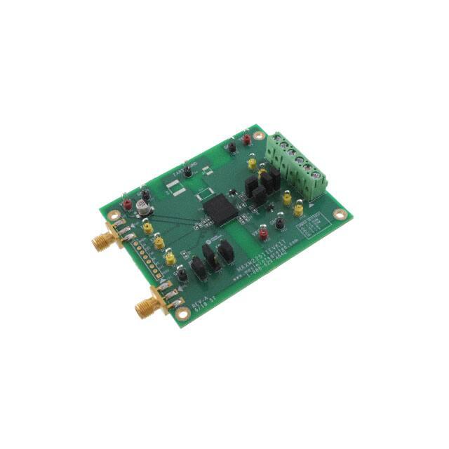
Evaluation Kit
Evaluates: MAXM22510/MAXM22511
General Description
Startup Procedure
The MAXM22510/MAXM22511 evaluation kit (EV kit) is a
fully assembled and tested PCB that demonstrates the
functionality of the MAXM22510/MAXM22511 isolated
RS-485/RS-422 transceiver module. The EV kit operates
from a single 3.3V supply.
Features
●● Operates From a Single 3.3V Supply
●● Terminal Block Connectors for Easy RS-485/RS-422
Evaluation
●● Up to 2500VRMS Isolation for 60s
●● Fully Assembled and Tested
Quick Start
Required Equipment
●● MAXM22510/MAXM22511 EV kit
●● 3.3V, 300mA DC power supply
●● Signal/function generator
●● Oscilloscope
Ordering Information appears at end of data sheet.
319-100244; Rev 1; 1/19
The EV kit is fully assembled and tested. Follow the steps
below to verify board operation.
1) Set the DC power supply to 3.3V and connect the
DC power supply between the EV kits VDDA and
GNDA connectors.
2) Ensure that all jumpers are in their default positions
(see Table 1).
3) Turn on the power supply.
4) Set the signal/function generator to output a 100kHz
0-to-3.3V square wave.
NOTE: Set the signal/function generator to operate
with a high-impedance load. If needed, the R1 pad is
available to add a 50Ω impedance to ground.
5) Connect the signal/function generator to the TXD
test point.
6) Using the oscilloscope, verify that the Y, Z, and RXD
outputs switch as the TXD signal toggles.
�MAXM22510/MAXM22511
Evaluation Kit
Detailed Description of Hardware
The EV kit is a fully assembled and tested circuit board
for evaluating the MAXM22510/MAXM22511 isolated
RS-485/RS-422 transceiver module (U1). The EV kit
is designed to evaluate the MAXM22510/MAXM22511
alone or in a standard RS-485 configuration.
Powering the Board
The MAXM22510/MAXM22511 operates from a single
supply. Connect an external 3.3V supply to the VDDA test
point (TP6). Connect the ground terminal of the supply to
the GNDA test point (TP7). The integrated DC/DC in the
MAXM22510/MAXM22511 generates the isolated power
for the B-side/isolated side of the board.
Evaluating the Isolated RS-485 Interface
Driver and Receiver Enable Selection
The EV kit features two jumpers (J2 and J4) to enable/
disable the driver and receiver outputs.
To enable the driver outputs (Y and Z), set the J4 jumper
to 1-2 (‘H’). Set J4 to 2-3 to disable the Y and Z outputs.
To enable the receiver on the MAXM22510/MAXM22511,
set the J2 jumper to 2-3 (‘L’). Set J2 to 1-2 to disable the
receiver.
Enabling/Disabling Shutdown Mode
In shutdown mode, the internal DC/DC is disabled and no
power is generated on the isolated side of the board. The
J3 jumper is available to enable/disable shutdown mode
for the MAXM22510/MAXM22511. Set the J3 jumper to
2-3 for normal operation. Set J3 to 1-2 to enter shutdown
mode.
The SBA output is high impedance during shutdown and
is not pulled high. The R6 pad on the board is available to
add a pull-up resistor to SBA if SBA must be high when
the MAXM22510/MAXM22511 is in shutdown mode.
Evaluates: MAXM22510/MAXM22511
On-Board Resistor Configurations
To evaluate the MAXM22510/MAXM22511 at the endof-the-line in a RS-485/RS-422 bus, close J6 to connect
a 120Ω termination resistor (R3) between the A and B
RS-485 receiver inputs.
Close J5 to connect a 120Ω termination resistor (R2)
between the Y and Z driver outputs.
Pullup and pulldown resistors are generally used on the
receiver inputs to guarantee a known state in the event
that all nodes on the bus are in receive mode, or the
cable becomes disconnected. The exact value for these
resistors varies with the application. R7 and R9 pads are
provided for pullup and pulldown resistors on the Y and
Z lines. R10 and R12 pads provide for pullup and pulldown resistors on the A and B lines, if needed. The use
of any of these resistors is purely optional. Note that the
MAXM22510/MAXM22511 features true fail-safe receiver
inputs, which ensures that RXD is high when the receiver
inputs are shorted, open, or connected to an idle bus.
RS-485 Interface Protection
The MAXM22510/MAXM22511 RS-485 interface pins (Y,
Z, A and B) feature internal ESD protection up to ±35kV
ESD (HBM), ±18kV ESD (Air gap), ±8kV ESD (Contact).
SM712 TVS diodes have been added to the I/O lines for
added protection up to ±30kV ESD (Air) and ±30kV ESD
(Contact). The SMT712 is also rated for protection against
EFT up to 40A (5/50ns).
Optimized EMI Layout
The MAXM22510/MAXM22511 EV kit has been designed
for easy evaluation and is not optimized for EMI
performance/evaluation. See the Design Resources tab
on the MAXM22510/MAXM22511 web page for more
information about best design practices for optimum EMI
performance.
Loopback Configuration
The MAXM22510/MAXM22511 features one drive channel and one receive channel. Driver outputs are Y and Z
and receiver inputs are A and B. To configure the device
for loopback testing, close J7 and J8 to connect B to Z
and A to Y, respectively.
www.maximintegrated.com
Maxim Integrated │ 2
�Evaluates: MAXM22510/MAXM22511
MAXM22510/MAXM22511
Evaluation Kit
Table 1. Jumper Table (J2–J8)
JUMPER
SHUNT POSITION
J2
J3
J4
1-2
RE is high. The RS-485 receiver is disabled.
2-3*
RE is low. The RS-485 receiver is enabled.
1-2
SD is high. The MAXM22510/MAXM22511 is in shutdown mode.
2-3*
SD is low. The MAXM22510/MAXM22511 is not in shutdown mode.
1-2*
DE is high. The RS-485 driver outputs are enabled.
2-3
DE is low. The RS-485 driver outputs are disabled.
Open
J5
Closed*
Open
J6
Closed*
J7
J8
DESCRIPTION
Y and Z are not connected through the on-board 120Ω termination resistor.
Y and Z are connected through the on-board 120Ω termination resistor.
A and B are not connected through the on-board 120Ω termination resistor.
A and B are connected through the on-board 120Ω termination resistor.
Open*
B is not connected to Z.
Closed
B is connected to Z.
Open*
A is not connected to Y.
Closed
A is connected to Y.
*Default position.
Ordering Information
PART
TYPE
MAXM22510EVKIT#
EV Kit
MAXM22511EVKIT#
EV Kit
#Denotes RoHS compliant.
www.maximintegrated.com
Maxim Integrated │ 3
�Evaluates: MAXM22510/MAXM22511
MAXM22510/MAXM22511
Evaluation Kit
MAXM22510/MAXM22511 EV Kit Bill of Materials
ITEM REF_DES
DNI/DNP QTY MFG PART #
MANUFACTURER
VALUE
1 C7
-
1 EEE-HA1A470WR
PANASONIC
47UF
2 J2-J4
3 J5-J8
-
3 PCC03SAAN
4 PEC02SAAN
SULLINS
SULLINS
PCC03SAAN
PEC02SAAN
4 J9
-
1
5 J10, J11
6 R2, R3
-
2 142-0701-851
2 CRCW0603120RJN
1935200 PHOENIX CONTACT
JOHNSON COMPONENTS
VISHAY DALE
1935200
142-0701-851
120
7 TP1, TP2, TP3, TP13-TP16 -
7
5014 N/A
5014
8 TP4, TP7, TP8, TP10, TP11 -
5
5011 N/A
5011
9 TP6, TP9, TP12
5010 KEYSTONE
N/A
MAXM22510GLH+ OR
MAXM22511GLH+
-
3
10 U1
-
1 MAXM22510GLH+ OR MAXM22511GLH+
11 U2, U3
12 PCB
-
13 C1, C4, C6
DNP
SM712.TCT
2 SM712.TCT
SEMTECH
PCB
1 MAXM22510/MAXM22511
MAXIM
GRM188R71E105KA12;CGA3E1X7R1E105K;TM
K107B7105KA;06033C105KAT2A;GCM188R71E
0 105KA64
MURATA;TDK;TAIYO YUDEN;AVX;MURATA 1UF
14 C2, C3, C5
15 C10
16 C11
DNP
DNP
DNP
0 C1608X7R1E104K080AA
0 VJ2220Y332KXUSTX1
0 GA352QR7GF102KW01
17
18
19
20
21
TOTAL
J1
R1, R5
R4
R6
R7, R9, R10, R12
DNP
DNP
DNP
DNP
DNP
0
0
0
0
0
32
www.maximintegrated.com
PBC08SAAN
CRCW060349R9FK
CRCW12100000Z0
CRCW060310K0FK;ERJ-3EKF1002
CRCW06031K00FK;ERJ-3EKF1001
MAXIM
TDK
VISHAY VITRAMON
MURATA
0.1UF
3300PF
1000PF
SULLINS ELECTRONICS CORP.
VISHAY DALE
VISHAY DALE
VISHAY DALE;PANASONIC
VISHAY DALE;PANASONIC
PBC08SAAN
10K
1K
DESCRIPTION
CAPACITOR; SMT (CASE_C); ALUMINUM-ELECTROLYTIC; 47UF; 10V; TOL=20%;
MODEL=HA SERIES; TG=-40 DEGC to +105 DEGC; TC=
CONNECTOR; MALE; THROUGH HOLE; BREAKAWAY; STRAIGHT THROUGH; 3PINS; 65 DEGC TO +125 DEGC
CONNECTOR; MALE; THROUGH HOLE; BREAKAWAY; STRAIGHT; 2PINS
CONNECTOR; FEMALE; THROUGH HOLE; GREEN TERMINAL BLOCK; STRAIGHT;
6PINS
CONNECTOR; END LAUNCH JACK RECEPTACLE; BOARDMOUNT; STRAIGHT
THROUGH; 2PINS;
RESISTOR; 0603; 120 OHM; 5%; 200PPM; 0.10W; THICK FILM
TEST POINT; PIN DIA=0.125IN; TOTAL LENGTH=0.445IN; BOARD HOLE=0.063IN;
YELLOW; PHOSPHOR BRONZE WIRE SILVER PLATE FINISH;
TEST POINT; PIN DIA=0.125IN; TOTAL LENGTH=0.445IN; BOARD HOLE=0.063IN;
BLACK; PHOSPHOR BRONZE WIRE SILVER PLATE FINISH;
TEST POINT; PIN DIA=0.125IN; TOTAL LENGTH=0.445IN; BOARD HOLE=0.063IN;
RED; PHOSPHOR BRONZE WIRE SIL;
IC; TXRXMOD; 2.5KVRMS COMPLETE ISOLATED RS-485/RS-422 MODULE
TRANSCEIVER + POWER; LGA44
IC; PROT; ASYMMETRICAL TVS DIODE FOR EXTENDED COMMON-MODE RS-485;
SOT23-3
PCB:MAXM22510/MAXM22511
CAPACITOR; SMT (0603); CERAMIC CHIP; 1UF; 25V; TOL=10%; TG=-55 DEGC TO
+125 DEGC; TC=X7R
CAPACITOR; SMT (0603); CERAMIC CHIP; 0.1UF; 25V; TOL=10%; MODEL=C SERIES;
TG=-55 DEGC TO +125 DEGC; TC=X7R
CAP; SMT (2220); 3300PF; 10%; 250V; X7R; CERAMIC CHIP
CAP; SMT (2211); 1000PF; 10%; 250V; X7R; CERAMIC CHIP
CONNECTOR; MALE; THROUGH HOLE; BREAKAWAY; STRAIGHT; 8PINS; -65 DEGC
TO +125 DEGC
49.9 RESISTOR; 0603; 49.9 OHM; 1%; 100PPM; 0.10W; THICK FILM
0 RESISTOR; 1210; 0 OHM; 0%; JUMPER; 0.5W; THICK FILM
RESISTOR; 0603; 10K; 1%; 100PPM; 0.10W; THICK FILM
RESISTOR; 0603; 1K; 1%; 100PPM; 0.10W; THICK FILM
Maxim Integrated │ 4
�1
2
3
4
5
6
7
8
1
J10
142-0701-851
1
TXD
RXD
SD
/SBA
RXD
REB
DE
TXD
J4
J3
J2
2
R1
VDDA
DNI
TP3
VDDA
2
2
DE
SD
TXD
REB
DNI
R5
RXD
TP2
VDDA
/SBA
TP1
DNI
10K
R6
VDDA
TP6
C1
DNI
VDDA
TP8
TP7
VDDA
DNI
C2
1
+
2
VDDA
J11
142-0701-851
J1
DNI
2
4
3
5
2
4
3
5
1
3
1
3
1
3
C7
47UF
1
2
3
4
5
6
7
8
9
10
11
12
13
14
15
16
17
18
19
20
21
22
GNDB
GNDB
GNDB
GNDB
GNDA
GNDA
GNDA
GNDA
R4
GNDB
GNDA
DNI
GNDB
GNDA
DNI
C11
DNI
VLDO
DE
TP4
VRECT
SD
Z
Y
GNDB
TXD
RXD
RE
VDDB
A
SBA
B
I.C.
VDDB
GNDA
VDDA
GNDB
GNDA
NC
GNDB
GNDA
NC
GNDB
GNDA
NC
GNDB
GNDA
NC
GNDB
GNDA
C10
MAXM22510GLH+
MAXM22511GLH+
U1
TP11
TP10
TP9
44
43
42
41
40
39
38
37
36
35
34
33
32
31
30
29
28
27
26
25
24
23
VRECT
VDDB
DNI
C3
A
B
DNI
C4
VDDB
Y
Z
TP12
TP16
TP15
TP14
TP13
VRECT
3
R2
120
J5
2
2
REVISION - B
DATE - 01/2019
1
3
SM712.TCT
U3
R12
DNI
R10
DNI
VDDB
2
2
R3
120
J6
MAXM22510EVKIT_B
MAXM22511EVKIT_B
1
DNI
C6
PROJECT TITLE:
R9
DNI
R7
VDDB
1
DNI
1
SM712.TCT
U2
DNI
C5
3
www.maximintegrated.com
3
J7
J8
6
5
4
3
2
1
J9
MAXM22510/MAXM22511
Evaluation Kit
Evaluates: MAXM22510/MAXM22511
MAXM22510/MAXM22511 EV Kit Schematic
Maxim Integrated │ 5
�MAXM22510/MAXM22511
Evaluation Kit
Evaluates: MAXM22510/MAXM22511
MAXM22510/MAXM22511 EV Kit PCB Layout Diagrams
MAXM22510/MAXM22511 EV Kit—Top Silkscreen
MAXM22510/MAXM22511 EV Kit—Top
MAXM22510/MAXM22511 EV Kit—Bottom
MAXM22510/MAXM22511 EV Kit—Bottom Silkscreen
www.maximintegrated.com
Maxim Integrated │ 6
�MAXM22510/MAXM22511
Evaluation Kit
Evaluates: MAXM22510/MAXM22511
Revision History
REVISION
NUMBER
REVISION
DATE
PAGES
CHANGED
0
8/18
Initial release
1
1/19
Update the Title on all pages to add MAXM22510 and to all sections where MAXM22511
is also mentioned; updated Table 1, the Bill of Materials, Schematic, PCB Layout, and
added MAXM22510EVKIT# to the Ordering Information table
DESCRIPTION
—
1–7
For pricing, delivery, and ordering information, please contact Maxim Direct at 1-888-629-4642, or visit Maxim Integrated’s website at www.maximintegrated.com.
Maxim Integrated cannot assume responsibility for use of any circuitry other than circuitry entirely embodied in a Maxim Integrated product. No circuit patent licenses
are implied. Maxim Integrated reserves the right to change the circuitry and specifications without notice at any time.
Maxim Integrated and the Maxim Integrated logo are trademarks of Maxim Integrated Products, Inc.
© 2019 Maxim Integrated Products, Inc. │ 7
�