- Page
ANALOGDEVICES fAX-ON-DEMAND HOTLINE
r.
W
..
26
ANALOG
DEVICES
MicropowerOperational
Amplifier
Singleor DualSupply
0P-20
GENERAL DESCRIPTION
The OP-20 is a monolithic micropower operational amplifier
that can be operated from a single power supply of +SV to
+30V. or from dual supplies of :t2.5V to :!:15V.The input
voltage range extends to the negative rail. therefore input
signals down to zero volts can be accomodated when
operating from a single supply.
Precision performance in high-gain applications is readily
obtained when using the OP-20. The B/F grade features a
maximum input offset voltage of 250sN, minimum CMRR of
95dB, and open-loop gain of over 500,000. Quiescent supply
currentisa maximum of only 55p.Aat :t2.5V or80llA at:!:15V.
The low input offset, high gain, and low power consumption
brings precision performance to portable instruments. satellites. missile control systems, and many other batterypowered applications.
FEATURES
.
..
.
.
.
.
.
.
Low Supply Current.. .
.. , . .. , .. .. . .. . 55p.AMax
Single-Supply Operation.. . ,.. . . .. . .. . .. +5V to +30V
Dual-Supply Operation. .
.,
:t2.5V to :t15V
Low Input Offset Voltage. . . . . . . . . . . . . . . . .. 250sN Max
Low Input Offset Voltage Drift
1.5p.V{OC
Max
HighCommon-ModeInput Range. .. V- to V+(-1.5V)
HlghCMRRandPSRR
,
High Open-Loop Gain
No External Component. Required
741 Pinout and Nulling
Available in Die Form
100dBMln
12OdBMIn
OBS
ORDERING
TA
INFORMATION
=+25"C
YosMAX
(mY)
TQ.e9
250
OP20BJ.
OP20BZ
250
OP20FJ
OP20FZ
250
500
500
500
-
1000
1000
.
t
tt
-
OP2OGJ
-
OP20HJ
-
t
PACKAGE
CERDIP
B-PIN
-
OP2OCZ
OP2OGZ
-
OP2QHZ
-
OLE
PLASTIC
B-PIN
-
-
OP20FP
-
OP20GP
OP20HStt
OP20HP
OPERATING
TEMPERATURE
RANGE
PIN CONNECTIONS
MIL
TSE
IND
COM
MIL
IND
COM
XIND
XIND
For devices processed in total compliance to Mll.STD-883. add f883 alter part
number. Consult factory for 883 data sheet.
Burn-in is avaOable on commercial and industrial temperature range parts in
cerDIP, plastic DIP. and TO-can packages.
For availability and bum.in infOO'l1ationon SO and PlCC packages, contact
your local sales office.
EPOXY MINI-DIP
(P-Suffix)
a-PIN HERMETIC DIP
(Z-Suffix)
N.C
8
'V'
BAl
.
-IN 2
+IN 3
6 OUf
5 BAl
.
11- {CASE}
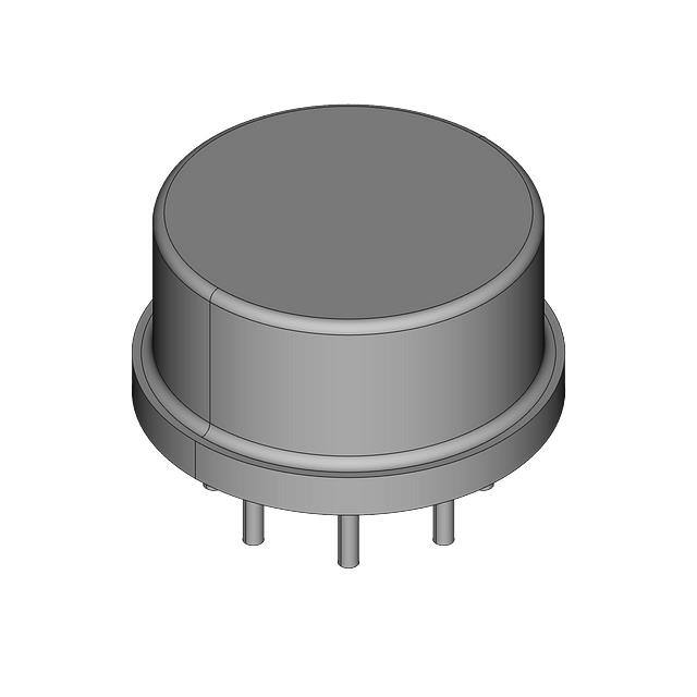
TO-99
(J-Suffix)
a-PIN SO
(S-Suffix)
SIMPLIFIED SCHEMATIC
v.
OUTPUT
-IN
-IN
013
033
v-
-1-
I
-~-
-
�ANALOGDEVICES fAX-ON-DEHAND HOTLINE
-
Page Z7
OP-20
ABSOLUTE MAXIMUMRATINGS (Note 1)
Supply Voltage
:t18V
DifferentialInputVoltage
:t30V
Input Voltage
Supply Voltage
Output Short-Circuit Duration
Indefinite
Storage Temperature Range
J and Z Packages
65°C to +150°C
P Package
65°C to +125°C
Operating Temperature Range
OP-20B, OP-20C (J, Z)
55°C to +125°C
OP-20F, OP-20G (J, Z)
25°C to +85°C
OP-20H (S, P. J. Z)
40°C to +85°C
OP-20FP, OP-2OGP
O°Cto +70°C
Lead Temperature Range (Soldering, 60 see)
300°C
Ju netionTemperature
,
OBS
PARAMETER
SYMBOL
CONDITIONS
Input Offset Voltage
Vos
Vs= t15V
Input Bias Current
'os
Ie
Input Voltage Range
IVA
VCM= 0
=+5V.
V- = OV
VS=t15V
V+=+5V, V-=OV
Common-Mode
RejectionRatio
PowerSupply
Rejeclion Retio
CMAR
OVVCM3.SV
Vs= :t15V
-15V$VCM13.5V
Vs= :t2.5Vto :tISV
PSRA
and V-
=OV.
AyO
tV:;; VoS 3.5V
VS=:t15V. Vo=:t10V
RL = 25kU
V+
Output Voltage
Swing
TO.99 (J)
150
18
.C/W
B-Pin Hermetic DIP (2)
148
16
.C/W
e.Pin Plastic DIP (P)
103
43
.C/W
B-Pin SO (S)
158
43
.C/W
NOTES:
1. Absolute maximum ratings apply to both DICE and packaged parts, unless
otherwise noted.
2. a'A is specified for worst case mounting conditions, i.e.. a'A is specified for
d~Yice in socket for TO, CerDIP and P-DIP packages; e.~ is specified for
device soldered to prlnled circuit board for SO package.
I
OP-20B/F
MIN
OP-20C/G
TYP
MAX
MIN
-
55
250
-
0.15
OP-20H
TYP
MAX
TYP
MAX
-
150
500
-
300
1000
1.5
-
0.2
2.5
-
0.3
4.0
Vo
Closed-Loop
Bandwidth
BW
Slew Rate
SR
Supply Current
ISY
= 5V. V- = OV
RL= 1OkU
Vs=:t1SV.
RL= 25kn
AyCL
=+1.0,
RL= 1Okfl
Vs=:t1SV
AL= 25kCl
Vs = :t2.5V,
No Load
Vs = :t15V,
No Load
MIN
nA
25
-
14
30
-
16
40
nA
0/3.5
-
-
-15/13.5
-
-
OLE
-
12
0/3.5
-
-
-15/13.5
-
-
95
105
-
90
95
-
100
110
-
94
105
-
-
4
6
-
6
300
500
-
200
500
1000
2000
-
800
2000
-
500
0,6/4.1
-
-
0,7/4.1
-
-
0.8/4.0
:t14.1
-
-
:t14.1
-
-
:t14.0
100
-
100
-
-
0.05
-
10
V+=SVto30V
V+=+SV, V-=OV
large-Signal
Voltage Gain
UNITS
SIC
at vs= :t2.5V to :t15V, TA= +25°C, unless otherwise noted.
VCM=O
V+
alA (NOTE 2)
-65°C to + 150°C
ELECTRICAL CHARACTERISTICS
Inpul Offset Current
PACKAGE TYPE
-
-
0.05
-
JAV
TE
0/3.5
- 15/13.5
V
-
65
90
90
100
-
10
dB
32
pVIV
500
V/mV
-
1000
V
100
0.05
kHz
-
-
40
55
-
44
63
-
45
70
-
55
60
-
57
85
-
60
95
-2-
UNITS
V/i-'S
i-'A
�ANALOGDEVICES fAX-ON-DEHAND HOTLINE
- Page 28
OP-20
ELECTRICAL CHARACTERISTICS at Vs .. :t2.5Vto:l:15V. -S5°C TA +125°C for OP-20BJIBZ and OP-20CZ, -25°C s TAS
+85°C for OP-20FJ/FZ and OP-20GJ/GZ. and DoC TA +70°C forOP.20FP. OP-20GP, and -40°C TA +85°C forOP-20HZ,Op.
20HJ. and OP-20HP/HS. unless otherwise noted.
OP-20C/G
OP.20B/F
MIN
TYP
MAX
MIN
PARAMETER
SYMBOL
CONDITIONS
Average Input
Offset Voltage
Drift {Note 1i
TCVos
Unnulled
-
0.75
Input OffsetVoltage
Vos
VS=:!:15V
-
155
400
-
-
0.5
2.5
-
-
12
27
-
-
-
-
-15/13.2
90
100
-
96
110
=0
Input Offset Current
109
VCIA
Input BiasCurrent
Is
VCI.I=O
Input Voltage
Range
'VA
0/3.2
V+=+5V. V-=OV
-15/13.2
Vs= :t15V
OBS
V+=+5V. V-= OV
Common-Mode
Rejection Ratio
CMAR
Power Supply
Rejection Ratio
PSRA
OVS VCMS 3.2V
Vs=:t15V
-15V S VCLIS 13.2V
Vs =:t2.5V to
:t1SV
V- = OV,
V+=SV to30V
Large-Signal
Voltage Gain
Avo
= SOkO
V+=5V.V-=OV.
Output Voltage
Swing
Vo
At = SOkll
Vs = :t1SV.
At =50kU
Vs =:t2.SV.No
Supply Current
lay
Load or +5V. OV
Vs = :t1SV,
No load
MIN
MAX
UNITS
7.0
!'v/oc
250
800
-
1.0
3.5
-
14
33
-
0/3.2
-
-
0/3.2
-
-
.15/13.2
85
90
-
80
85
-
90
105
-
85
100
4
10
-
8
18
-
10
32
4
10
6
18
-
10
57
600
-
250
-
0.8/4.0
-
-
0.9/3.9
-
-
1.0/3.8
:t14.0
-
-
:t13.9
-
-
:t13.9
-
50
65
53
75
-
64
95
68
100
NOTE:
,. Sample tested.
400
-
1.5
500
1700
!'V
1.5
5.0
nA
16
45
nA
V
-
dB
700
500
TYP
-
1.0
OLE
Vs=:t1SV.Vo= :t10V
Rt
-
OP-20H
MAX
3.0
1.5
-
TYP
!'V/V
400
-
V/mV
..-...,..,.-
.
TE
-
-
55
85
72
115
v
!'A
-3-
~
~
�-
ANALOGDEVICES fAX-ON-DEMAND HOTLINE
Page
28
OP-20
DICE CHARACTERISTICS
1.
2.
3.
4.
5.
6.
7.
BALANCE
INVERTINGINPUT
NONINVERTINGINPUT
VBALANCE
OUTPUT
V+
DIE SIZE 0.069 X 0.047 Inch, 3174 sq. mils
(1.75 x 1.17 mm,2.05 sq. mm)
OBS
WAFER TEST LIMITS at Vs= :I::15V,TA=25°C, unless otherwise noted.
PARAMETER
SYMBOL
Input Offset Yoltage
Yos
Input Offset Current
'os
Inpul Bias Current
Ie
Input Yoltage Range
IVR
Common-Mode
Rejection Ratio
Power Supply
Rejection Ratio
Large-Signal
Voltage Gain
CONDITIONS
Y+=+Sy,
V-=OY
Vs":!:ISV
CMRR
V+=+SV, V-=OV,OV:SVCM:S+3.5V
Vs = :!:15V,-15V
VCM:S:!:13.5V
Vs=:!:2.5Vto:!:15V
PSRR
OLE
Op.20N
V-
= OV,
V+
OP-20G
LIMIT
LIMIT
300
600
1000
jJYMAX
1.5
2.5
4.0
nA MAX
25
30
0/3.5
-15/13.5
0/3.5
-15/13.5
95
100
90
94
10
6
= +5V
to +3OV
AyO
Output Voltage
Swing
Vo
Supply Current
tSY
RL
= 25kfi
OP-20GR
LIMIT
UNITS
TE
40
nA MAX
0/3.5
-15/13.5
VMIN
85
90
dBMIN
32
jJ.V/V MAX
500
VlmV MIN
0.8/4.1
:t 14.1
0.9/4.0
:t 14.0
VMjN
63
85
70
95
jJAMAX
1000
800
0.7/4.1
:t14.1
55
80
Vo=::!:10V
RL
= 10kO,V+ = +5V, V- = OV
RL
= 25kO,
Vs = ::!:15V
Vs = ::!:2.5V,No Load
Vs = ::!:15V,No Load
NOTE:
Electrical tests are performed at wafer probe to the limits shown. Due to variations in assembly methods and normal yield loss, yield after packaging is not
guaranteed for standard product dice. Consult factory to negotiate specifications based on dice lot qualification through sample lot assembly and testing.
TYPICAL ELECTRICAL CHARACTERISTICS
at Vs= :t 15V,TA= +250C. unless otherwise noted.
OP-20N
PARAMETER
SYMBOL
CONDITIONS
Average Input
Offset Voltage Drift
TCVos
TCVosn
Unnulled
Large-Signal
Voltage Gain
AyO
RL = 25kO
Nulled, Rp: 10kO
OP-20G
OP-20GR
TYPICAL
TYPICAL
TYPICAL
UNITS
1.0
1.0
1.5
1.5
2.5
2.5
p.V/oC
2000
2000
1000
V/mV
-4--~
�ANALOGDEVICES fAX-ON-DEHAND HOTLINE
-
- Page 3a
OP-20
TYPICAL PERFORMANCE CHARACTERISTICS
150
125
I--
'"
«
~
0
75
>
t;; 50
:r
...
0
.. 25
::>
/
J
V
-25
,/
110
....
z
w
6
~
~
4
..-
4O
20
20
0
0
.s
0
-20
.,5
.10
0.01
- '- l
I
u
;>-30
-'
"-
---
,/
./
~
~200
"-
.....-
/'
V
~
~
2
0
-100
0
50
TEMPERATUREr"C)
SMALL-SIGNAL
100
TRANSIENT
150
20
10
100
-50
TE
60
1
~400
::>
u
....
!i!300
...
100k
101<
SUPPLY CURRENT
va SUPPLY VOLTAGE
INPUTOFFSET CURRENT
;500
Z
Iii
....
10
100
,.
fREQUENCY 1Hz)
1.0
SUPPLY VOL TAGE IVOLTSI
OLE
I
I
I
liS. >1511
12
60
Z
2
~
175
25
15
125
TEMPERATURE(oCI
14
~
80
NULLED TO ZERO OFFSET AT 25"c
WITH IOk POT
INPUT BIAS CURRENT
va TEMPERATURE
8
100
~ 80
0
::t;;
'" 60
...
...
0
40
OBS
~
120
:;:
.:>100
~
«
1/
\\
""-.
::>
(,)
120
.
g
-25
-75
140
liS'