a
Low-Noise, Precision
Operational Amplifier
OP27
PIN CONNECTIONS
FEATURES
Low Noise: 80 nV p-p (0.1 Hz to 10 Hz), 3 nV/÷Hz
Low Drift: 0.2 �V/�C
High Speed: 2.8 V/�s Slew Rate, 8 MHz Gain
Bandwidth
Low VOS: 10 �V
Excellent CMRR: 126 dB at VCM of ±11 V
High Open-Loop Gain: 1.8 Million
Fits 725, OP07, 5534A Sockets
Available in Die Form
TO-99
(J-Suffix)
BAL
BAL 1
OP27
V+
OUT
–IN 2
NC
+IN 3
GENERAL DESCRIPTION
4V– (CASE)
NC = NO CONNECT
The OP27 precision operational amplifier combines the low
offset and drift of the OP07 with both high speed and low noise.
Offsets down to 25 mV and maximum drift of 0.6 mV/∞C, makes
the OP27 ideal for precision instrumentation applications.
Exceptionally low noise, en = 3.5 nV/÷Hz, at 10 Hz, a low 1/f
noise corner frequency of 2.7 Hz, and high gain (1.8 million),
allow accurate high-gain amplification of low-level signals. A
gain-bandwidth product of 8 MHz and a 2.8 V/msec slew rate
provides excellent dynamic accuracy in high-speed, dataacquisition systems.
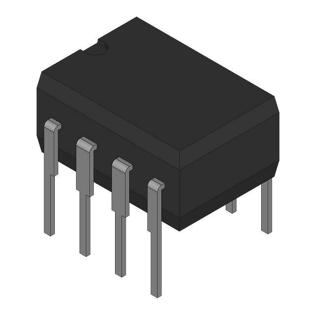
8-Pin Hermetic DIP
(Z-Suffix)
Epoxy Mini-DIP
(P-Suffix)
8-Pin SO
(S-Suffix)
A low input bias current of ± 10 nA is achieved by use of a
bias-current-cancellation circuit. Over the military temperature
range, this circuit typically holds IB and IOS to ±20 nA and 15 nA,
respectively.
VOS TRIM 1
The output stage has good load driving capability. A guaranteed
swing of ± 10 V into 600 W and low output distortion make the
OP27 an excellent choice for professional audio applications.
8
VOS TRIM
–IN 2
7
V+
+IN 3
6
OUT
V– 4
5
NC
OP27
NC = NO CONNECT
(Continued on page 7)
SIMPLIFIED SCHEMATIC
V+
R3
Q6
R1*
1
8
VOS ADJ.
C2
R4
Q22
R2*
R23
Q21
Q24
Q23
Q46
C1
R24
R9
Q20
Q1A
Q1B
Q2B
Q19
OUTPUT
R12
Q2A
NONINVERTING
INPUT (+)
C3
R5
C4
Q3
INVERTING
INPUT (–)
Q11
Q26
Q12
Q27
Q45
Q28
*R1 AND R2 ARE PERMANENTLY
ADJUSTED AT WAFER TEST FOR
MINIMUM OFFSET VOLTAGE.
V–
REV. C
Information furnished by Analog Devices is believed to be accurate and
reliable. However, no responsibility is assumed by Analog Devices for its
use, nor for any infringements of patents or other rights of third parties that
may result from its use. No license is granted by implication or otherwise
under any patent or patent rights of Analog Devices. Trademarks and
registered trademarks are the property of their respective companies.
One Technology Way, P.O. Box 9106, Norwood, MA 02062-9106, U.S.A.
Tel: 781/329-4700
www.analog.com
Fax: 781/326-8703
© 2003 Analog Devices, Inc. All rights reserved.
�OP27–SPECIFICATIONS
ELECTRICAL CHARACTERISTICS (@ V = ±15 V, T = 25�C, unless otherwise noted.)
S
Conditions
A
Min
OP27A/E
Typ Max
Min
OP27F
Typ Max
Min
OP27C/G
Typ Max
Parameter
Symbol
Unit
INPUT OFFSET
VOLTAGE1
VOS
10
25
20
60
30
100
mV
LONG-TERM VOS
STABILITY2, 3
VOS/Time
0.2
1.0
0.3
1.5
0.4
2.0
mV/MO
INPUT OFFSET
CURRENT
IOS
7
35
9
50
12
75
nA
INPUT BIAS
CURRENT
IB
± 10
± 40
± 12
± 55
± 15
± 80
nA
INPUT NOISE
VOLTAGE3, 4
en p-p
0.1 Hz to 10 Hz
0.08
0.18
0.08
0.18
0.09
0.25
mV p-p
INPUT NOISE
Voltage Density3
en
fO = 10 Hz
fO = 30 Hz
fO = 1000 Hz
3.5
3.1
3.0
5.5
4.5
3.8
3.5
3.1
3.0
5.5
4.5
3.8
3.8
3.3
3.2
8.0
5.6
4.5
nV/÷Hz
nV/÷Hz
nV/÷Hz
INPUT NOISE
Current Density3, 5
in
fO = 10 Hz
fO = 30 Hz
fO = 1000 Hz
1.7
1.0
0.4
4.0
2.3
0.6
1.7
1.0
0.4
4.0
2.3
0.6
1.7
1.0
0.4
0.6
pA/÷Hz
pA/÷Hz
pA/÷Hz
INPUT
RESISTANCE
Differential-Mode6
Common-Mode
RIN
RINCM
1.3
INPUT VOLTAGE
RANGE
IVR
± 11.0 ± 12.3
± 11.0 ± 12.3
± 11.0 ± 12.3
V
114
106
100
dB
COMMON-MODE
REJECTION RATIO CMRR
VCM = ± 11 V
POWER SUPPLY
PSRR
REJECTION RATIO
VS = ± 4 V
to ± 18 V
LARGE-SIGNAL
VOLTAGE GAIN
RL ≥ 2 kW,
VO = ± 10 V
RL ≥ 600 W,
VO = ± 10 V
AVO
6
3
0.94
126
1
10
5
2.5
0.7
123
1
10
4
2
MW
GW
120
2
20
mV/V
1000
1800
1000
1800
700
1500
V/mV
800
1500
800
1500
600
1500
V/mV
OUTPUT
VOLTAGE SWING
VO
RL ≥ 2 kW
RL ≥ 600 W
± 12.0 ± 13.8
± 10.0 ± 11.5
± 12.0 ± 13.8
± 10.0 ± 11.5
± 11.5 ± 13.5
± 10.0 ± 11.5
V
V
SLEW RATE7
SR
RL ≥ 2 kW
1.7
2.8
1.7
2.8
1.7
2.8
V/ms
GAIN
BANDWIDTH
PRODUCT7
GBW
5.0
8.0
5.0
8.0
5.0
8.0
MHz
OPEN-LOOP
OUTPUT
RESISTANCE
RO
VO = 0, IO = 0
70
70
W
POWER
CONSUMPTION
Pd
VO
90
RP = 10 kW
± 4.0
OFFSET
ADJUSTMENT
RANGE
70
140
90
± 4.0
140
100
± 4.0
170
mW
mV
NOTES
1
Input offset voltage measurements are performed ~ 0.5 seconds after application of power. A/E grades guaranteed fully warmed up.
2
Long-term input offset voltage stability refers to the average trend line of V OS versus. Time over extended periods after the first 30 days of operation. Excluding the
initial hour of operation, changes in V OS during the first 30 days are typically 2.5 mV. Refer to typical performance curve.
3
Sample tested.
4
See test circuit and frequency response curve for 0.1 Hz to 10 Hz tester.
5
See test circuit for current noise measurement.
6
Guaranteed by input bias current.
7
Guaranteed by design.
–2–
REV. C
�OP27
ELECTRICAL CHARACTERISTICS
(@ VS = ±15 V, –55�C £ TA £ 125�C, unless otherwise noted.)
Symbol
INPUT OFFSET
VOLTAGE1
VOS
30
60
TCVOS2
TCVOSn3
0.2
INPUT OFFSET
CURRENT
IOS
INPUT BIAS
CURRENT
IB
INPUT VOLTAGE
RANGE
IVR
AVERAGE INPUT
OFFSET DRIFT
Conditions
Min
OP27A
Typ
Parameter
Max
Min
OP27C
Typ
Max
Unit
70
300
mV
0.6
4
1.8
mV/∞C
15
50
30
135
nA
± 20
± 60
± 35
± 150
nA
± 10.3
± 11.5
± 10.2
± 11.5
V
108
122
94
118
dB
COMMON-MODE
REJECTION RATIO CMRR
VCM = ± 10 V
POWER SUPPLY
REJECTION RATIO PSRR
VS = ± 4.5 V to ± 18 V
2
LARGE-SIGNAL
VOLTAGE GAIN
AVO
RL ≥ 2 kW, VO = ± 10 V 600
1200
300
800
V/mV
OUTPUT
VOLTAGE SWING
VO
RL ≥ 2 kW
± 13.5
± 10.5
± 13.0
V
± 11.5
16
4
51
mV/V
NOTES
1
Input offset voltage measurements are performed by automated test equipment approximately 0.5 seconds after application of power. A/E grades guaranteed fully
warmed up.
2
The TCVOS performance is within the specifications unnulled or when nulled with R P = 8 kW to 20 kW. TCVOS is 100% tested for A/E grades, sample tested for
C/F/G grades.
3
Guaranteed by design.
REV. C
–3–
�OP27
ELECTRICAL CHARACTERISTICS
(@ VS = ±15 V, –25�C¯£ TA £ 85�C for OP27J, OP27Z, 0�C £ TA £ 70�C for OP27EP,
OP27FP, and –40�C £ TA £ 85�C for OP27GP, OP27GS, unless otherwise noted.)
VOS
20
50
40
140
55
220
mV
TCVOS1
TCVOSn2
0.2
0.2
0.6
0.6
0.3
0.3
1.3
1.3
04
04
1.8
1.8
mV/∞C
mV/∞C
INPUT OFFSET
CURRENT
IOS
10
50
14
85
20
135
nA
INPUT BIAS
CURRENT
IB
± 14
± 60
± 18
± 95
± 25
± 150
nA
INPUT VOLTAGE
RANGE
IVR
POWER SUPPLY
REJECTION RATIO PSRR
LARGE-SIGNAL
VOLTAGE GAIN
OUTPUT
VOLTAGE SWING
AVO
VO
VCM = ± 10 V
Max
Min
Min
OP27G
Typ Max
INPUT ONSET
VOLTAGE
COMMON-MODE
REJECTION RATIO CMRR
Min
OP27F
Typ Max
Symbol
AVERAGE INPUT
OFFSET DRIFT
Conditions
OP27E
Typ
Parameter
Unit
± 10.5
± 11.8
± 10.5 ± 11.8
± 10.5 ± 11.8
V
110
124
102
96
dB
VS = ± 4.5 V
to ± 18 V
2
15
121
2
RL ≥ 2 kW,
VO = ± 10 V
750
1500
700
RL ≥ 2 kW
± 11.7
± 13.6
± 11.4 ± 13.5
1300
16
118
2
450
1000
± 11.0 ± 13.3
32
mV/V
V/mV
V
NOTES
1
The TCVOS performance is within the specifications unnulled or when nulled with R P = 8 kW to 20 kW. TCVOS is 100% tested for A/E grades, sample tested for
C/F/G grades.
2
Guaranteed by design.
–4–
REV. C
�OP27
DIE CHARACTERISTICS
1.
2.
3.
4.
6.
7.
8.
1
1990
1427U
8
NULL
(–) INPUT
(+) INPUT
V–
OUTPUT
V+
NULL
2
3
7
6
4
WAFER TEST LIMITS
(@ VS = ±15 V, TA = 25�C unless otherwise noted.)
OP27N
Limit
OP27G
Limit
OP27GR
Limit
Unit
VOS
35
60
100
mV Max
INPUT OFFSET CURRENT
IOS
35
50
75
nA Max
INPUT BIAS CURRENT
IB
± 40
± 55
± 80
nA Max
INPUT VOLTAGE RANGE
IVR
± 11
± 11
± 11
V Min
COMMON-MODE REJECTION
RATIO
CMRR
VCM = IVR
114
106
100
dB Min
POWER SUPPLY
PSRR
VS = ± 4 V to ± 18 V
10
10
20
mV/V Max
AVO
AVO
RL ≥ 2 kW, VO = ± 10 V
RL ≥ 600 W, VO = ± 10 V
1000
800
1000
800
700
600
V/mV Min
V/mV Min
OUTPUT VOLTAGE SWING
VO
VO
RL ≥ 2 kW
RL2600n
± 12.0
± 10.0
± 12.0
± 10.0
+11.5
± 10.0
V Min
V Min
POWER CONSUMPTION
Pd
VO = 0
140
140
170
mW Max
Parameter
Symbol
INPUT OFFSET VOLTAGE*
LARGE-SIGNAL VOLTAGE
GAIN
Conditions
NOTE
*Electrical tests are performed at wafer probe to the limits shown. Due to variations in assembly methods and normal yield loss, yield after packaging is not guaranteed
for standard product dice. Consult factory to negotiate specifications based on dice lot qualification through sample lot assembly and testing.
REV. C
–5–
�OP27
TYPICAL ELECTRICAL CHARACTERISTICS (@ V = ±15 V, T = 25�C unless otherwise noted.)
S
Parameter
AVERAGE INPUT OFFSET
VOLTAGE DRIFT*
Symbol
Conditions
TCVOS or
TCVOSn
Nulled or Unnulled
RP = 8 kW to 20 kW
A
OP27N
Typical
OP27G
Typical
OP27GR
Typical
Unit
0.2
0.3
0.4
mV/∞C
AVERAGE INPUT OFFSET
CURRENT DRIFT
TCIOS
80
130
180
pA/∞C
AVERAGE INPUT BIAS
CURRENT DRIFT
TCIB
100
160
200
pA/∞C
INPUT NOISE VOLTAGE
DENSITY
en
en
en
fO = 10 Hz
fO = 30 Hz
fO = 1000 Hz
3.5
3.1
3.0
3.5
3.1
3.0
3.8
3.3
3.2
nV/÷Hz
nV/÷Hz
nV/÷Hz
in
in
in
fO = 10 Hz
fO = 30 Hz
fO = 1000 Hz
1.7
1.0
0.4
1.7
1.0
0.4
1.7
1.0
0.4
pA/÷Hz
pA/÷Hz
pA/÷Hz
INPUT NOISE VOLTAGE
SLEW RATE
enp-p
SR
0.1 Hz to 10 Hz
RL ≥ 2 kW
0.08
2.8
0.08
2.8
0.09
2.8
mV p-p
V/ms
GAIN BANDWIDTH
PRODUCT
GBW
8
8
8
MHz
INPUT NOISE CURRENT
DENSITY
NOTE
*Input offset voltage measurements are performed by automated test equipment approximately 0.5 seconds after application of power.
–6–
REV. C
�OP27
(Continued from page 1)
The OP27 provides excellent performance in low-noise, highaccuracy amplification of low-level signals. Applications include
stable integrators, precision summing amplifiers, precision voltagethreshold detectors, comparators, and professional audio circuits
such as tape-head and microphone preamplifiers.
PSRR and CMRR exceed 120 dB. These characteristics, coupled
with long-term drift of 0.2 mV/month, allow the circuit designer
to achieve performance levels previously attained only by discrete designs.
The OP27 is a direct replacement for 725, OP06, OP07, and
OP45 amplifiers; 741 types may be directly replaced by removing the 741’s nulling potentiometer.
Low-cost, high-volume production of OP27 is achieved by
using an on-chip Zener zap-trimming network. This reliable
and stable offset trimming scheme has proved its effectiveness
over many years of production history.
ABSOLUTE MAXIMUM RATINGS 4
Supply Voltage . . . . . . . . . . . . . . . . . . . . . . . . . . . . . . . ± 22 V
Input Voltage1 . . . . . . . . . . . . . . . . . . . . . . . . . . . . . . . ± 22 V
Output Short-Circuit Duration . . . . . . . . . . . . . . . . Indefinite
Differential Input Voltage2 . . . . . . . . . . . . . . . . . . . . . . ± 0.7 V
Differential Input Current2 . . . . . . . . . . . . . . . . . . . . ± 25 mA
Storage Temperature Range . . . . . . . . . . . . –65∞C to +150∞C
Operating Temperature Range
OP27A, OP27C (J, Z) . . . . . . . . . . . . . . . . –55∞C to +125∞C
OP27E, OP27F (J, Z) . . . . . . . . . . . . . . . . . –25∞C to +85∞C
OP27E, OP27F (P) . . . . . . . . . . . . . . . . . . . . . . 0∞C to 70∞C
OP27G (P, S, J, Z) . . . . . . . . . . . . . . . . . . –40∞C to +85∞C
Lead Temperature Range (Soldering, 60 sec) . . . . . . . 300∞C
Junction Temperature . . . . . . . . . . . . . . . . . –65∞C to +150∞C
Package Type
�JA3
�JC
Unit
TO 99 (J)
8-Lead Hermetic DlP (Z)
8-Lead Plastic DIP (P)
20-Contact LCC (RC)
8-Lead SO (S)
150
148
103
98
158
18
16
43
38
43
∞C/W
∞C/W
∞C/W
∞C/W
∞C/W
NOTES
1
For supply voltages less than ± 22 V, the absolute maximum input voltage is
equal to the supply voltage.
2
The OP27’s inputs are protected by back-to-back diodes. Current limiting
resistors are not used in order to achieve low noise. If differential input voltage
exceeds ± 0.7 V, the input current should be limited to 25 mA.
3
JA is specified for worst-case mounting conditions, i.e., JA is specified for
device in socket for TO, CERDIP, and P-DIP packages; JA is specified for
device soldered to printed circuit board for SO package.
4
Absolute Maximum Ratings apply to both DICE and packaged parts, unless
otherwise noted.
ORDERING INFORMATION 1
Package
TA = 25∞C
VOS Max
(mV)
25
25
60
100
100
100
TO-99
CERDIP
8-Lead
OP27AJ2, 3
OP27EJ2, 3
OP27AZ2
OP27EZ
OP27GJ
OP27CZ3
OP27GZ
Plastic
8-Lead
OP27EP
OP27FP3
OP27GP
OP27GS4
Operating
Temperature
Range
MIL
IND/COM
IND/COM
MIL
XIND
XIND
NOTES
1
Burn-in is available on commercial and industrial temperature range parts in CERDIP, plastic
DIP, and TO-can packages.
2
For devices processed in total compliance to MIL-STD-883, add /883 after part number.
Consult factory for 883 data sheet.
3
Not for new design; obsolete April 2002.
4
For availability and burn-in information on SO and PLCC packages, contact your local
sales office.
CAUTION
ESD (electrostatic discharge) sensitive device. Electrostatic charges as high as 4000 V readily
accumulate on the human body and test equipment and can discharge without detection. Although
the OP27 features proprietary ESD protection circuitry, permanent damage may occur on devices
subjected to high-energy electrostatic discharges. Therefore, proper ESD precautions are
recommended to avoid performance degradation or loss of functionality.
REV. C
–7–
WARNING!
ESD SENSITIVE DEVICE
�OP27–Typical Performance Characteristics
VOLTAGE NOISE – nV/ Hz
90
70
60
50
TEST TIME OF 10sec FURTHER
LIMITS LOW FREQUENCY
(1 V), the output waveform will look as shown in the
pulsed operation diagram (Figure 3).
During the fast feedthrough-like portion of the output, the input
protection diodes effectively short the output to the input and a
current, limited only by the output short-circuit protection, will
be drawn by the signal generator. With Rf ≥ 500 W, the output is
capable of handling the current requirements (IL £ 20 mA at 10 V);
the amplifier will stay in its active mode and a smooth transition
will occur.
When Rf > 2 kW, a pole will be created with Rf and the amplifier’s
input capacitance (8 pF) that creates additional phase shift and
reduces phase margin. A small capacitor (20 pF to 50 pF) in
parallel with R f will eliminate this problem.
Rf
–
OP27
2.8V/�s
+
Figure 3. Pulsed Operation
COMMENTS ON NOISE
The OP27 is a very low-noise monolithic op amp. The outstanding
input voltage noise characteristics of the OP27 are achieved mainly
by operating the input stage at a high quiescent current. The input
OP08/108
2
OP07
10
5
1 RS
e.g. RS
2 RS
e.g. RS
5534
OP27/37
1
50
RS1
REGISTER
NOISE ONLY
100
UNMATCHED
= R S1 = 10k�, R S2 = 0
MATCHED
= 10k�, R S1 = R S2 = 5k�
RS2
10k
500
1k
5k
RS – SOURCE RESISTANCE – �
50k
Figure 4. Noise vs. Source Resistance (Including Resistor
Noise) at 1000 Hz
At RS