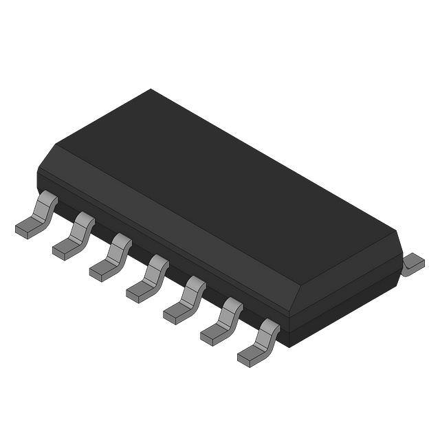
OP481GSZ-REEL7

OP481GSZ-REEL7

  • 厂商:

    AD(亚德诺)

  • 封装:

    SOIC14_150MIL

  • 描述:

    超低功耗、轨到轨输出运算放大器(四通道)

  • 详情介绍
  • 数据手册
  • 价格&库存
OP481GSZ-REEL7 数据手册
Ultralow Power, Rail-to-Rail Output Operational Amplifiers OP281/OP481 FEATURES Low supply current: 4 μA/amplifier maximum Single-supply operation: 2.7 V to 12 V Wide input voltage range Rail-to-rail output swing Low offset voltage: 1.5 mV No phase reversal PIN CONFIGURATIONS OUT A 1 –IN A 2 8 V+ APPLICATIONS Comparator Battery-powered instrumentation Safety monitoring Remote sensors Low voltage strain gage amplifiers OUT A –IN A +IN A V– 1 Figure 1. 8-Lead Narrow-Body SOIC (R Suffix) 8 V+ OUT B –IN B +IN B 00291-002 2 3 4 OP281 TOP VIEW (Not to Scale) 7 6 5 GENERAL DESCRIPTION The OP281 and OP481 are dual and quad ultralow power single-supply amplifiers featuring rail-to-rail outputs. Each operates from supplies as low as 2.0 V and is specified at +3 V and +5 V single supplies as well as ±5 V dual supplies. Fabricated on Analog Devices’ CBCMOS process, the OP281/OP481 feature a precision bipolar input and an output that swings to within millivolts of the supplies, continuing to sink or source current up to a voltage equal to the supply voltage. Applications for these amplifiers include safety monitoring, portable equipment, battery and power supply control, and signal conditioning and interfacing for transducers in very low power systems. The output’s ability to swing rail-to-rail and not increase supply current when the output is driven to a supply voltage enables the OP281/OP481 to be used as comparators in very low power systems. This is enhanced by their fast saturation recovery time. Propagation delays are 250 μs. The OP281/OP481 are specified over the extended industrial temperature range (−40°C to +85°C). The OP281 dual amplifier is available in 8-lead SOIC surface-mount and TSSOP packages. The OP481 quad amplifier is available in narrow 14-lead SOIC and TSSOP packages. Figure 2. 8-Lead TSSOP (RU Suffix) OUT A 1 –IN A 2 +IN A 3 V+ 4 14 OUT D 13 –IN D OP481 12 +IN D 11 V– TOP VIEW (Not to Scale) 10 +IN C +IN B 5 00291-003 00291-004 –IN B 6 OUT B 7 9 8 –IN C OUT C Figure 3. 14-Lead Narrow-Body SOIC (R Suffix) OUT A –IN A +IN A V+ +IN B –IN B OUT B 1 2 3 4 5 6 7 14 OUT D 13 –IN D 12 +IN D OP481 TOP VIEW 11 V– (Not to Scale) 10 +IN C 9 8 –IN C OUT C Figure 4. 14-Lead TSSOP (RU Suffix) Rev. C Information furnished by Analog Devices is believed to be accurate and reliable. However, no responsibility is assumed by Analog Devices for its use, nor for any infringements of patents or other rights of third parties that may result from its use. Specifications subject to change without notice. No license is granted by implication or otherwise under any patent or patent rights of Analog Devices. Trademarks and registered trademarks are the property of their respective owners. One Technology Way, P.O. Box 9106, Norwood, MA 02062-9106, U.S.A. Tel: 781.329.4700 www.analog.com Fax: 781.461.3113 ©1996–2007 Analog Devices, Inc. All rights reserved. 00291-001 OUT B TOP VIEW +IN A 3 (Not to Scale) 6 –IN B 5 +IN B V– 4 7 OP281 OP281/OP481 TABLE OF CONTENTS Features .............................................................................................. 1 Applications....................................................................................... 1 Pin Configurations ........................................................................... 1 General Description ......................................................................... 1 Revision History ............................................................................... 2 Specifications..................................................................................... 3 Electrical Specifications............................................................... 3 Absolute Maximum Ratings............................................................ 6 Thermal Resistance ...................................................................... 6 ESD Caution.................................................................................. 6 Typical Performance Characteristics ............................................. 7 Applications..................................................................................... 13 Theory of Operation .................................................................. 13 Input Overvoltage Protection ................................................... 13 Input Offset Voltage ................................................................... 13 Input Common-Mode Voltage Range ..................................... 13 Capacitive Loading..................................................................... 14 Micropower Reference Voltage Generator.............................. 14 Window Comparator................................................................. 14 Low-Side Current Monitor ....................................................... 15 Low Voltage Half-Wave and Full-Wave Rectifiers................. 15 Battery-Powered Telephone Headset Amplifier..................... 15 Outline Dimensions ....................................................................... 17 Ordering Guide .......................................................................... 18 REVISION HISTORY 10/07—Rev. B to Rev. C Updated Format..................................................................Universal Changes to Offset Voltage Drift Condition .................................. 3 Changes to Slew Rate Symbol ......................................................... 5 Changes to Figure 8.......................................................................... 7 Deleted SPICE Macro-Model Section ......................................... 13 Updated Outline Dimensions ....................................................... 17 Changes to Ordering Guide .......................................................... 18 3/03—Rev. A to Rev. B Changes to Features.......................................................................... 1 2/03—Rev. 0 to Rev. A Updated Format..................................................................Universal Deleted OP181 ....................................................................Universal Updated Package Options .................................................Universal Deleted OP181 Pin Configurations ................................................1 Deleted Epoxy DIP Pin Configurations .........................................1 Changes to Absolute Maximum Ratings........................................5 Changes to Ordering Guide .............................................................5 Changes to Input Offset Voltage................................................... 10 Deleted Former Figure 33 ............................................................. 10 Deleted Overdrive Recovery Time Section................................. 11 Deleted Former Figure 36 ............................................................. 11 Deleted 8-Lead and 14-Lead Plastic DIP (N-8 and N-14) Outline Dimensions ....................................................................... 14 Updated Outline Dimensions....................................................... 14 Rev. C | Page 2 of 20 OP281/OP481 SPECIFICATIONS ELECTRICAL SPECIFICATIONS VS = 3.0 V, VCM = 1.5 V, TA = 25°C, unless otherwise noted. Table 1. Parameter INPUT CHARACTERISTICS Offset Voltage 1 Input Bias Current Input Offset Current Input Voltage Range Common-Mode Rejection Ratio Large-Signal Voltage Gain Offset Voltage Drift Bias Current Drift Offset Current Drift OUTPUT CHARACTERISTICS Output Voltage High Output Voltage Low Short-Circuit Limit POWER SUPPLY Power Supply Rejection Ratio Supply Current/Amplifier DYNAMIC PERFORMANCE Slew Rate Turn-On Time Saturation Recovery Time Gain Bandwidth Product Phase Margin NOISE PERFORMANCE Voltage Noise Voltage Noise Density Current Noise Density 1 Symbol VOS IB IOS CMRR AVO ΔVOS/∆T ΔIB/ΔT ΔIOS/ΔT VOH VOL ISC PSRR ISY Condition Min Typ Max 1.5 2.5 10 7 2 Unit mV mV nA nA V dB V/mV V/mV μV/°C pA/°C pA/°C V mV mA dB μA μA V/ms μs μs μs kHz Degrees μV p-p nV/√Hz pA/√Hz −40°C ≤ TA ≤ +85°C −40°C ≤ TA ≤ +85°C −40°C ≤ TA ≤ +85°C VCM = 0 V to 2.0 V, −40°C ≤ TA ≤ +85°C RL = 1 MΩ, VO = 0.3 V to 2.7 V −40°C ≤ TA ≤ +85°C −40°C to +85°C 0 65 5 2 3 0.1 95 13 10 20 2 2.925 2.96 25 ±1.1 95 3 RL = 100 kΩ to GND, −40°C ≤ TA ≤ +85°C RL = 100 kΩ to V+, −40°C ≤ TA ≤ +85°C 75 VS = 2.7 V to 12 V, −40°C ≤ TA ≤ +85°C VO = 0 V −40°C ≤ TA ≤ +85°C RL = 100 kΩ, CL = 50 pF AV = 1, VO = 1 V AV = 20, VO = 1 V 76 4 5 SR GBP φM en p-p en in 0.1 Hz to 10 Hz f = 1 kHz 25 40 50 65 95 70 10 75
OP481GSZ-REEL7
1. 物料型号: - OP281: 双路超低功耗单电源放大器 - OP481: 四路超低功耗单电源放大器

2. 器件简介: - OP281和OP481分别提供双路和四路超低功耗放大,它们可以从低至2.0V的电源供电,并在+3V和+5V单电源以及±5V双电源下工作。这些放大器在非常低的电源系统中,如安全监控、便携设备、电池和电源控制以及在极低功耗系统中对传感器进行信号调理和接口等方面有广泛应用。

3. 引脚分配: - 提供了8引脚SOIC和TSSOP封装的引脚配置图(见Figure 1和Figure 2)以及14引脚SOIC和TSSOP封装的引脚配置图(见Figure 3和Figure 4)。

4. 参数特性: - 低功耗:每个放大器最大4μA - 单电源操作:2.7V至12V - 宽输入电压范围 - 轨到轨输出摆动 - 低偏置电压:1.5mV,无相位反转

5. 功能详解: - 这些放大器能够在输出驱动至供电轨时仍保持低功耗,使其可以用作极低功耗系统的比较器。此外,它们快速的饱和恢复时间也增强了这一功能。 - 传播延迟为250μs,OP281/OP481在扩展工业温度范围(-40°C至+85°C)内都有规定。

6. 应用信息: - 比较器、电池供电仪器、安全监控、远程传感器、低电压应变计放大器等。

7. 封装信息: - OP281双路放大器提供8引脚SOIC表贴和TSSOP封装。 - OP481四路放大器提供窄体14引脚SOIC和TSSOP封装。

OP481GSZ-REEL7 价格&库存

很抱歉,暂时无法提供与“OP481GSZ-REEL7”相匹配的价格&库存,您可以联系我们找货

免费人工找货