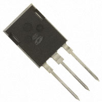
TYPICAL PERFORMANCE CURVES ®
APT50GN120B2 APT50GN120B2G*
APT50GN120B2(G) 1200V
*G Denotes RoHS Compliant, Pb Free Terminal Finish.
Utilizing the latest Non-Punch Through (NPT) Field Stop technology, these IGBT’s have a very short, low amplitude tail current and low Eoff. The Trench Gate design results in superior VCE(on) performance. Easy paralleling results from very tight parameter distribution and slightly positive VCE(on) temperature coefficient. Built-in gate resistance ensures ultra-reliable operation. Low gate charge simplifies gate drive design and minimizes losses.
(B2)
T-Max®
• • • •
• 1200V NPT Field Stop
Trench Gate: Low VCE(on) Easy Paralleling 10µs Short Circuit Capability Intergrated Gate Resistor: Low EMI, High Reliability
C G E
Applications: Welding, Inductive Heating, Solar Inverters, SMPS, Motor drives, UPS
MAXIMUM RATINGS
Symbol VCES VGE I C1 I C2 I CM SSOA PD TJ,TSTG TL Parameter Collector-Emitter Voltage Gate-Emitter Voltage Continuous Collector Current
8
All Ratings: TC = 25°C unless otherwise specified.
APT50GN120B2(G) UNIT Volts
1200 ±30
@ TC = 25°C
134 66 150 150A @ 1200V 543 -55 to 150 300
Watts °C Amps
Continuous Collector Current @ TC = 110°C Pulsed Collector Current
1
@ TC = 150°C
Switching Safe Operating Area @ TJ = 150°C Total Power Dissipation Operating and Storage Junction Temperature Range Max. Lead Temp. for Soldering: 0.063" from Case for 10 Sec.
STATIC ELECTRICAL CHARACTERISTICS
Symbol V(BR)CES VGE(TH) VCE(ON) Characteristic / Test Conditions Collector-Emitter Breakdown Voltage (VGE = 0V, I C = 400µA) Gate Threshold Voltage (VCE = VGE, I C = 2mA, Tj = 25°C) MIN TYP MAX Units
1200 5 1.4
2 2
5.8 1.7 1.9
6.5 2.1
Collector-Emitter On Voltage (VGE = 15V, I C = 50A, Tj = 25°C) Collector-Emitter On Voltage (VGE = 15V, I C = 50A, Tj = 125°C) Collector Cut-off Current (VCE = 1200V, VGE = 0V, Tj = 25°C)
Volts
I CES I GES RGINT
100 TBD 600 4
Gate-Emitter Leakage Current (VGE = ±20V) Intergrated Gate Resistor
nA Ω
CAUTION: These Devices are Sensitive to Electrostatic Discharge. Proper Handling Procedures Should Be Followed.
APT Website - http://www.advancedpower.com
050-7602
Rev C
10-2005
Collector Cut-off Current (VCE = 1200V, VGE = 0V, Tj = 125°C)
µA
�DYNAMIC CHARACTERISTICS
Symbol Cies Coes Cres VGEP Qg Qge Qgc SSOA SCSOA td(on) td(off) tf Eon1 Eon2 Eoff td(on) tr td(off) tf Eon1 Eon2 Eoff tr Characteristic Input Capacitance Output Capacitance Reverse Transfer Capacitance Gate-to-Emitter Plateau Voltage Total Gate Charge
3
APT50GN120B2(G)
Test Conditions Capacitance VGE = 0V, VCE = 25V f = 1 MHz Gate Charge VCE = 600V I C = 50A TJ = 150°C, R G = 2.2Ω 7, VGE = 15V, L = 100µH,VCE = 1200V TJ = 125°C, R G = 2.2Ω 7 VCC = 960V, VGE = 15V, VGE = 15V MIN TYP MAX UNIT pF V nC
3600 210 170 9.5 315 20 190 150 10 28 27 320 115 TBD 3900 4495 28 27 395 205 TBD 5660 6795 µJ
ns ns A
Gate-Emitter Charge Gate-Collector ("Miller ") Charge Switching Safe Operating Area Short Circuit Safe Operating Area Turn-on Delay Time Current Rise Time Turn-off Delay Time Current Fall Time Turn-on Switching Energy Turn-off Switching Energy Turn-on Delay Time Current Rise Time Turn-off Delay Time Current Fall Time Turn-on Switching Energy Turn-off Switching Energy
44 55 4 5
µs
Inductive Switching (25°C) VCC = 800V VGE = 15V I C = 50A
RG = 2.2Ω 7 TJ = +25°C
Turn-on Switching Energy (Diode)
6
µJ
Inductive Switching (125°C) VCC = 800V VGE = 15V I C = 50A
Turn-on Switching Energy (Diode)
66
TJ = +125°C
RG = 2.2Ω 7
THERMAL AND MECHANICAL CHARACTERISTICS
Symbol RθJC RθJC WT Characteristic Junction to Case (IGBT) Junction to Case (DIODE) Package Weight MIN TYP MAX UNIT °C/W gm
.23 N/A 5.9
1 Repetitive Rating: Pulse width limited by maximum junction temperature. 2 For Combi devices, Ices includes both IGBT and FRED leakages 3 See MIL-STD-750 Method 3471. 4 Eon1 is the clam ped inductive turn-on-energy of the IGBT only, without the effect of a commutating diode reverse recovery current adding to the IGBT turn-on loss. (See Figure 24.) 5 Eon2 is the clamped inductive turn-on energy that includes a commutating diode reverse recovery current in the IGBT turn-on switching loss. (See Figures 21, 22.)
10-2005 Rev C
6 Eoff is the clamped inductive turn-off energy measured in accordance with JEDEC standard JESD24-1. (See Figures 21, 23.) 7 RG is external gate resistance, not including RGint nor gate driver impedance. 8 Continuous current limited by package lead temperature.
APT Reserves the right to change, without notice, the specifications and information contained herein.
050-7602
�TYPICAL PERFORMANCE CURVES
160 140 IC, COLLECTOR CURRENT (A) 120 100 80 60 40 20 0
160
15V
APT50GN120B2(G)
15V
IC, COLLECTOR CURRENT (A)
140
12V 11V
120 100
12V 11V
10V 9V 8V
80 60 40 20 0
10V 9V 8V 7V
160 140 120 100
FIGURE 1, Output Characteristics(TJ = 25°C)
250µs PULSE TEST
很抱歉,暂时无法提供与“APT50GN120B2G”相匹配的价格&库存,您可以联系我们找货
免费人工找货