140 COMMERCE DRIVE MONTGOMERYVILLE, PA 18936-1013 PHONE: (215) 631-9840 FAX: (215) 631-9855
MRF544
RF & MICROWAVE DISCRETE LOW POWER TRANSISTORS
Features
• • • • Silicon NPN, high Frequency, high breakdown Transistor Maximum Unilateral Gain = 13.5 dB (typ) @ f = 200 MHz High Collector Base Breakdown Voltage - BVCBO = 100 V (min) High FT - 1400 MHz
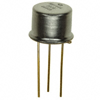
1. Emitter 2. Base 3. Collector
TO-39
DESCRIPTION:
Designed primarily for use in high frequency and medium and high resolution color video display monitors as well as other applications requiring high breakdown characteristics.
ABSOLUTE MAXIMUM RATINGS (Tcase = 25°C)
Symbol VCEO VCBO VEBO IC Parameter Collector-Emitter Voltage Collector-Base Voltage Emitter-Base Voltage Collector Current Value 70 100 3.0 400 Unit Vdc Vdc Vdc mA
Thermal Data
P
D Total Device Dissipation @ TA = 25ºC Derate above 25ºC 3.5 20 Watts mW/ ºC
Advanced Power Technology reserves the right to change, without notice, the specifications and information contained herein
Visit our website at WWW.ADVANCEDPOWER.COM or contact our factory direct.
�MRF544
ELECTRICAL SPECIFICATIONS (Tcase = 25°C)
STATIC (off)
Symbol BVCEO BVCBO BVEBO ICBO ICES Test Conditions Min. Collector-Emitter Breakdown Voltage (IC = 1.0 mAdc, IB = 0) Collector-Base Breakdown Voltage (IC= 100 µAdc, IE=0) Emitter-Base Breakdown Voltage (IE = 100 µAdc, IC = 0) Collector Cutoff Current (VCE = 80 Vdc, IE = 0 Vdc) Collector Cutoff Current (VCE = 80 Vdc, IE = 0 Vdc) 70 100 3.0 Value Typ. 1.0 Max. 20 100 Unit Vdc Vdc Vdc µA µA
(on)
HFE DC Current Gain (IC = 50 mAdc, VCE = 6.0 Vdc) 15 -
DYNAMIC
Symbol Test Conditions Min. COB CIB fT Output Capacitance (VCB = 10Vdc, IE=0, f=1 MHz) Input Capacitance (VEB = 3Vdc, IE=0, f=1 MHz) Current-Gain - Bandwidth Product (IC = 50 mAdc, VCE = 10 Vdc, f = 250 MHz) 1000 Value Typ. 2.5 6.1 1500 Max. Unit pF pF MHz
Advanced Power Technology reserves the right to change, without notice, the specifications and information contained herein
Visit our website at WWW.ADVANCEDPOWER.COM or contact our factory direct.
�MRF544
FUNCTIONAL
Symbol Test Conditions Min. Maximum Unilateral Gain Maximum Available Gain Insertion Gain
IC = 50 mAdc, VCE = 25Vdc, f = 200 MHz IC = 50 mAdc, VCE = 25Vdc, f = 200 MHz IC = 50 mAdc, VCE = 25Vdc, f = 200 MHz
Value Typ. 13.5 13.5 12.7 Max. Unit dB dB dB
G
U max
11.7
MAG
2
|S21|
Table 1. Common Emitter S-Parameters, @ VCE = 25 V, IC = 50 mA
f S11 S21 S12 S22
(MHz)
100 200 300 400 500 600 700 800 900 1000
|S11| 0.221 0.219 0.250 0.329 0.338 0.348 0.371 0.374 0.402 0.438
∠φ -143 -108 -72 -34 9 51 94 140 -170 -126
|S21| 8.54 4.36 2.98 2.39 2.11 1.83 1.61 1.44 1.45 1.56
∠φ 97 87 79 72 70 65 61 59 63 64
|S12| 0.047 0.091 0.141 0.178 0.237 0.292 0.35 0.383 0.428 0.503
∠φ 82 87 87 84 87 86 86 85 88 86
|S22| 0.508 0.413 0.406 0.445 0.409 0.412 0.411 0.413 0.386 0.405
∠φ 14 49 82 108 140 176 -147 -112 -78 -42
Advanced Power Technology reserves the right to change, without notice, the specifications and information contained herein
Visit our website at WWW.ADVANCEDPOWER.COM or contact our factory direct.
�MRF544
Advanced Power Technology reserves the right to change, without notice, the specifications and information contained herein
Visit our website at WWW.ADVANCEDPOWER.COM or contact our factory direct.
�
很抱歉,暂时无法提供与“MRF544”相匹配的价格&库存,您可以联系我们找货
免费人工找货