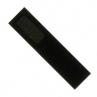
Solderable Silicon Photodiodes PDB-C601-1
PACKAGE DIMENSIONS[mm] [mm] CHIP DIMENSIONS INCH INCH
.030 [0.76] .021 [0.53] .014 [0.36]
.040 [1.02]
.125 [3.18] .074 [1.88] ACTIVE AREA
CHIP DIMENSIONS INCH [mm]
.022 [0.56] ACTIVE AREA
SOLDERABLE PHOTODIODE
BARE SHIP PACKAGE
FEATURES
DESCRIPTION
• • • •
APPLICATIONS
Optical encoder Position sensor Industrial controls Instrumentation
• Red enhanced The PDB-C601-1 is a silicon red enhanced • Photocondutctive solderable photodiode designed for low capacitance • High quantum efficiency and high speed for photoconductive applications.
ABSOLUTE MAXIMUM RATING (TA)= 23°C UNLESS OTHERWISE NOTED
VBR TSTG TO TS Reverse Voltage Storage Temperature Operating Temperature Soldering Temperature* -40 -40 75 +125 +100 +224 V °C °C °C
Responsivity (A/W)
SPECTRAL RESPONSE
0.80 0.70 0.60 0.50 0.40 0.30 0.20 0.10 0.00 250 300 350 400 450 500 550 600 650 700 750 800 850 900 950 1000 1050 1100 Wavelength (nm) 1150
SYMBOL
PARAMETER
MIN
MAX
UNITS
* 1/16 inch from case for 3 seconds max.
ELECTRO-OPTICAL CHARACTERISTICS RATING (TA)= 23°C UNLESS OTHERWISE NOTED
SYMBOL ISC ID RSH CJ lrange VBR NEP tr CHARACTERISTIC Short Circuit Current Dark Current Shunt Resistance Junction Capacitance Spectral Application Range Breakdown Voltage Noise Equivalent Power Response Time TEST CONDITIONS H = 100 fc, 2850 K VR = 5 V VR = 10 mV VR = 5 V, f = 1 MHz Spot Scan I = 10 μA VR = 0V @ l=Peak RL = 1KΩ,VR = 5V MIN 15 60 350 25 TYP 17 0.5 150 10 50 1x10-14 10 MAX 2 UNITS μA nA MW pF nm V W/ √ Hz nS
1100
**Response time of 10% to 90% is specified at 660nm wavelength light.
Information in this technical datasheet is believed to be correct and reliable. However, no responsibility is assumed for possible inaccuracies or omission. Specifications are subject to change without notice.
Advanced Photonix Inc. 1240 Avenida Acaso, Camarillo CA 93012 • Phone (805) 987-0146 • Fax (805) 484-9935 • www.advancedphotonix.com
�
很抱歉,暂时无法提供与“PDB-C601-1”相匹配的价格&库存,您可以联系我们找货
免费人工找货