Advance Information
This document contains information on a product under development. The parametric information
contains target parameters that are subject to change.
M20001
High Bandwidth Dual 2:1 Mux/DeMux Passive Switch
The M20001 is a high bandwidth, low power, dual differential single pole, double throw switch. Both switches are
controlled using a single select pin. Due to the very high bandwidth of the device, it can be used for routing and
switching of very high-speed NRZ data.
The M20001 is offered in an industry standard, green and RoHS compliant, 3 mm x 3 mm QFN package. The
device pinout is architected to enable optimized PCB routing while providing maximum crosstalk isolation.
Crosstalk isolation is critical for successful data transmission at multi-gigabit speeds.
The M20001 operates from a single 3.3 V power supply. This supply is used to operate the switch control only,
therefore, the M20001 consumes less than 2 mW of power during normal operation.
Applications
• Two differential, single pole, double throw switches
• 10G Ethernet
• Low insertion loss
• PCI Express Gen 3 — 8.0 Gbps
• 6 GHz 3 dB bandwidth
• SAS/SATA
• Very low power consumption
• DisplayPort 1.2 — 5.4 Gbps
• Superior crosstalk isolation
• USB 3.0 — 5 Gbps
• 3 x 3 mm, 16-pin QFN package
• 3G SDI
• 3.3 V supply voltage, no additional regulation needed
• FibreChannel - 8.5 Gbps
Advance Information
Features
• Industrial temp range -40 to 85 °C
M20001
VDD
50k
100k
Port1a+
Port1b+
Port1aPort1b-
50k
Port1-
V DD
100k
Port1+
Port0a+
Port0b+
Port0aPort0b-
50k
Port0-
100k 100k
Port0+
50k
Switch Control Diagram and Typical Application Diagram
Control
20001-DSH-001-E
Mindspeed Technologies®
Mindspeed Proprietary and Confidential
January 2014
�Ordering Information
Part Number
Package
Operating Case Temperature
M20001G-14*
3x3 mm, 16-pin QFN package
-40 °C to 85 °C
* The letter “G” designator after the part number indicates that the device is RoHS compliant. Refer to www.mindspeed.com for additional
information. The RoHS compliant devices are backwards compatible with 225 °C reflow profiles.
Revision History
Revision
Level
Date
Description
E
Advance
January 2014
D
Advance
April 2013
C
Advance
February 2012
Updated Front page Applications
Updated specifications in Table 1-3 and Table 1-4.
Revised Figure 1-1.
Updated Ordering Information (added 13P).
Advance Information
Table 1-1: VESD, HBM maximum updated to 2000 V.
Removed VESD, CDM and VESD, mm.
Table 1-3: IDD maximum updated to 600 µA; PTOTAL maximum updated to 2.2 mW.
Table 1-4: tSKEW, PN typical updated to 5 ps.
ΔRON typical updated to 0.55 Ω.
ΔRON, CH typical updated to 0.45 Ω.
Removed IOUT_SHORT and VOUT_OPEN.
Chapter 2: Updated all Insertion/Return Loss charts.
B
Advance
April 2011
Revised product title.
A
Advance
January 2011
Advance release.
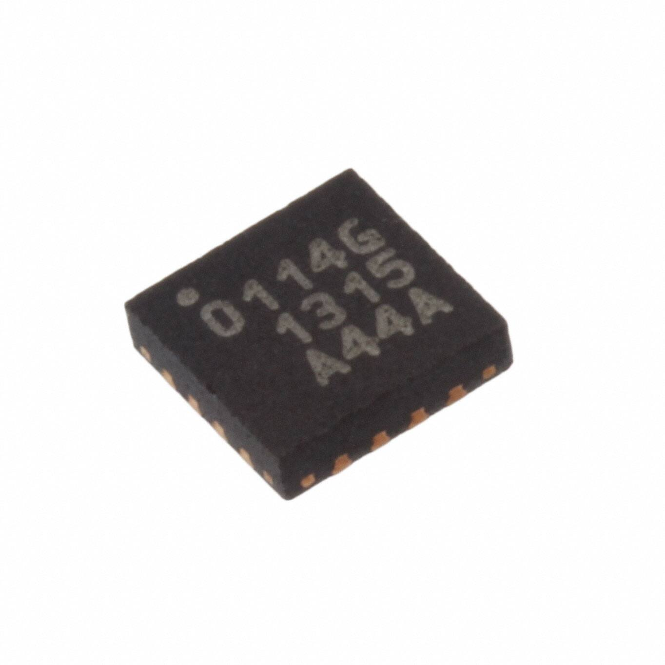
M20001 Marking Diagrams
01rrG
Device Number (1st 2 digits – part number “01”, digits 3 and 4 are device
revision, and “G” indicates ROHS compliant device
YYWW
Date Code
ZZZZZ
Manufacturing lot number
NOTE: Early device samples may be labeled as AP and BP to identify early lot numbers , lot number
identified as A or B and “P” for prototype
20001-DSH-001-E
Mindspeed Technologies®
Mindspeed Proprietary and Confidential
2
�1.0 Electrical Characteristics
Unless noted otherwise, test conditions in this section are: VDD = 3.3 V, 25 °C case temperature, 800 mV
differential input data swing (VIH, DATA = 200 mV), nominal (800 mVPPD) output swing, PRBS 27- 1 test pattern with
RLOAD = 50 Ω, short traces and/or cables.
Table 1-1.
Absolute Maximum Ratings
Symbol
Parameter
VDD
VESD, HBM
ISW
Table 1-2.
Minimum
Typical
Maximum
Unit
Supply voltage
-0.5
—
4
V
Storage temperature
-65
150
°C
Electrostatic discharge voltage (HBM)
—
—
2000
V
DC current on data pins
—
—
4
mA
Note
Minimum
Typical
Maximum
Unit
Supply voltage
—
2.97
3.3
3.63
V
Operating case temperature
—
-40
—
85
°C
—
—
3
mA
Note
Minimum
Typical
Maximum
Unit
Quiescent power supply current
—
—
100
500
µA
DC power consumption
—
—
0.33
1.8
mW
Note
Minimum
Typical
Maximum
Unit
Recommended Operating Conditions
Symbol
Parameter
VDD
TCASE
DC current on data pins
ISW
Table 1-3.
Power Consumption Specifications
Symbol
Parameter
IDD
PTOTAL
Table 1-4.
Advance Information
TSTORE
Note
Input/Output Electrical Characteristics
Symbol
Parameter
VIH
Input high voltage on VSEL pin
1
0.7 x VDD
—
VDD
V
VIL
Input low voltage on VSEL pin
1
0
—
0.3 x VDD
V
Differential peak to peak input data swing (AC-coupled)
—
—
—
2.8
V
VIH, DATA
Input high voltage on data pins, VPEAK, AC-coupled
—
—
—
700
mV
VCM, DATA
Common-mode voltage on data pins if DC-coupled (VDD/3)
—
0.99
1.1
1.21
V
Switching time
1
—
0.3
0.5
µs
VPPD
SW
20001-DSH-001-E
Mindspeed Technologies®
Mindspeed Proprietary and Confidential
3
�Electrical Characteristics
Table 1-4.
Input/Output Electrical Characteristics
Symbol
Parameter
Note
Minimum
Typical
Maximum
Unit
tSKEW, PN
Bit-to-bit skew within the same differential pair
—
8
15
ps
tSKEW, CH
Channel-to-channel skew
—
12
25
ps
3 dB bandwidth
5.6
6
—
GHz
XTALK
Crosstalk 0 - 6 GHz (Port 0 to Port 1)
—
-30
-25
dB
OIRR
Off Isolation 0 - 6 GHz (PortX to PortXa with PortXb enabled)
24
26
—
dB
SDD21
Insertion loss @ DC
—
0.7
1.25
dB
SDD11
Differential return loss 50 MHz - 1.25 GHz
12.5
14
—
dB
SDD11
Differential return loss 1.25 GHz - 2.5 GHz
8
9
—
dB
SDD11
Differential return loss 2.5 GHz - 4 GHz
5
8
—
dB
SCM11
Common mode return loss 50 MHz - 2.5 GHz
12
14
—
dB
SCM11
Common mode return loss 2.5 GHz - 4 GHz
10.5
13
—
dB
BW
On resistance of the switch
—
8.5
15.5
Ω
∆RON
On resistance match between same pair
—
0.3
0.5
Ω
∆RON, CH
On resistance match between channels
—
0.3
0.8
Ω
Advance Information
RON
NOTES:
1. Control pin specifications.
Figure 1-1.
Enable and Disable Timing Diagram
VSEL
V
DD
/2
V
DD
V
/2
DD
GND
t
PortXa
SW
t
SW
VMAX = 0.7V
VCM, DC
t
SW
t
SW
VCM, DC
PortXb
The timing diagram above shows the response of the high signal path when the VSEL pin is switched. When VSEL
is set low PortXb will be disabled after time tSW and PortXa will be enabled after time tSW.
20001-DSH-001-E
Mindspeed Technologies®
Mindspeed Proprietary and Confidential
4
�2.0 Typical Performance
Characteristics
Unless noted otherwise, test conditions in this section are: VDD = 3.3 V, 25 °C case temperature, 800 mV
differential input data swing (VIH, DATA = 200 mV), nominal (800 mVPPD) output swing, PRBS 27- 1 test pattern with
RLOAD = 50 Ω, short traces and/or cables, AC-coupled I/O.
Eye Diagram at 5 Gbps, 2 dB of
De-emphasis
Figure 2-2.
Eye Diagram at 8 Gbps, 2 dB of
De-emphasis
Figure 2-3.
Eye Diagram at 10 Gbps, 2 dB of
De-emphasis
Figure 2-4.
Eye Diagram at 12 Gbps, 2 dB of
De-emphasis
20001-DSH-001-E
Mindspeed Technologies®
Mindspeed Proprietary and Confidential
Advance Information
Figure 2-1.
5
�Typical Performance Characteristics
Insertion Loss as a Function of
Temperature, Port 0 to Port 0b
Figure 2-6.
Insertion Loss as a Function of
Supply Voltage, Port 0 to Port 0b
Figure 2-7.
Return Loss as a Function of
Temperature, Port 0 to Port 0b
Figure 2-8.
Return Loss as a Function of Supply
Voltage, Port 0 to Port 0b
20001-DSH-001-E
Mindspeed Technologies®
Mindspeed Proprietary and Confidential
6
Advance Information
Figure 2-5.
�Typical Performance Characteristics
Figure 2-9.
Insertion Loss as a Function of
Temperature, Port 0 to Port 0a
20001-DSH-001-E
Insertion Loss as a Function of
Supply Voltage, Port 0 to Port 0a
Figure 2-12. Return Loss as a Function of Supply
Voltage, Port 0 to Port 0a
Mindspeed Technologies®
Mindspeed Proprietary and Confidential
7
Advance Information
Figure 2-11. Return Loss as a Function of
Temperature, Port 0 to Port 0a
Figure 2-10.
�Typical Performance Characteristics
Figure 2-14. Insertion Loss as a Function of
Supply Voltage, Port 1 to Port 1b
Figure 2-15. Return Loss as a Function of
Temperature, Port 1 to Port 1b
Figure 2-16. Return Loss as a Function of Supply
Voltage, Port 1 to Port 1b
20001-DSH-001-E
Mindspeed Technologies®
Mindspeed Proprietary and Confidential
8
Advance Information
Figure 2-13. Insertion Loss as a Function of
Temperature, Port 1 to Port 1b
�Typical Performance Characteristics
Figure 2-18. Insertion Loss as a Function of
Supply Voltage, Port 1 to Port 1a
Figure 2-19. Return Loss as a Function of
Temperature, Port 1 to Port 1a
Figure 2-20. Return Loss as a Function of Supply
Voltage, Port 1 to Port 1a
20001-DSH-001-E
Mindspeed Technologies®
Mindspeed Proprietary and Confidential
9
Advance Information
Figure 2-17. Insertion Loss as a Function of
Temperature, Port 1 to Port 1a
�Typical Performance Characteristics
Figure 2-22. Isolation as a Function of
Temperature, Opposite Channels
Figure 2-23. Isolation as a Function of Supply
Voltage, Same Channels
Figure 2-24. Isolation as a Function of
Temperature, Same Channels
20001-DSH-001-E
Mindspeed Technologies®
Mindspeed Proprietary and Confidential
Advance Information
Figure 2-21. Isolation as a Function of Supply
Voltage, Opposite Channels
10
�3.0 Pin Description, Pinout, and
Package Outline Drawing
The M20001 is assembled in a 3 x 3 mm, 16-pin QFN package. The package paddle is used to provide the device
ground connection as well as a thermal path.
Figure 3-1.
M20001 Package Outline Drawing
ALL DIMENSIONS ARE IN MILLIMETERS
1.700±0.050
Exp.DAP
Advance Information
3.000±0.050
PIN 1 DOT
BY MARKING
PIN #1 IDENTIFICATION
CHAMFER 0.300 X 45˚
0.375±0.050
3.000±0.050
0.500 Bsc
16L T/SLP
(3x3mm)
1.700±0.050
Exp.DAP
0.230±0.050
1.500
Ref.
TOP VIEW
BOTTOM VIEW
NOTE:
1) TSLP AND SLP SHARE THE SAME EXPOSE OUTLINE
BUT WITH DIFFERENT THICKNESS:
A
20001-DSH-001-E
TSLP
SLP
MAX.
0.800
0.900
NOM.
0.750
0.850
MIN.
0.700
0.800
0.203 Ref.
0.000-0.050
TOP VIEW
Mindspeed Technologies®
Mindspeed Proprietary and Confidential
11
�Pin Description, Pinout, and Package Outline Drawing
PORT0aN
1
PORT0aP
2
PORT1aN
PORT1bP
PORT1bN
M20001 Pinout Diagram (Top View Shown)
PORT1aP
Figure 3-2.
16
15
14
13
12
VDD
11
PORT1N
PORT1P
M20001
16-PIN QFN
(3 x 3 mm)
9
5
6
7
8
GND
4
PORT0N
PORT0bP
PORT0P
10
VDD
3
Advance Information
Table 3-1.
PORT0bN
VSEL
M20001 Pin Descriptions
Pin Name
Pin Number(s)
Type
Description
PORT0aN
1
RF port
Analog switch 0a, N
PORT0aP
2
RF port
Analog switch 0a, P
PORT0bN
3
RF port
Analog switch 0b, N
PORT0bP
4
RF port
Analog switch 0b, P
VDD
5, 12
Power
Positive supply voltage input
PORT0P
6
RF port
Analog switch 0, P
PORT0N
7
RF port
Analog switch 0, N
GND
8
Ground
Ground
VSEL
9
Control input
Control signal input:
Low: Port A enabled
High: Port B enabled
PORT1P
10
RF port
Analog switch 1, P
PORT1N
11
RF port
Analog switch 1, N
PORT1bN
13
RF port
Analog switch 1b, N
PORT1bP
14
RF port
Analog switch 1b, P
PORT1aN
15
RF port
Analog switch 1a, N
PORT1aP
16
RF port
Analog switch 1a, P
20001-DSH-001-E
Mindspeed Technologies®
Mindspeed Proprietary and Confidential
12
�www.mindspeed.com
General Information:
Telephone: (949) 579-3000
Headquarters - Newport Beach
4000 MacArthur Blvd., East Tower
Newport Beach, CA 92660
Information in this document is provided in connection with Mindspeed Technologies® ("Mindspeed®") products.
These materials are provided by Mindspeed as a service to its customers and may be used for informational
purposes only. Except as provided in Mindspeed’s Terms and Conditions of Sale for such products or in any
separate agreement related to this document, Mindspeed assumes no liability whatsoever. Mindspeed assumes
no responsibility for errors or omissions in these materials. Mindspeed may make changes to specifications and
product descriptions at any time, without notice. Mindspeed makes no commitment to update the information and
shall have no responsibility whatsoever for conflicts or incompatibilities arising from future changes to its
specifications and product descriptions. No license, express or implied, by estoppel or otherwise, to any
intellectual property rights is granted by this document.
THESE MATERIALS ARE PROVIDED "AS IS" WITHOUT WARRANTY OF ANY KIND, EITHER EXPRESS OR
IMPLIED, RELATING TO SALE AND/OR USE OF MINDSPEED PRODUCTS INCLUDING LIABILITY OR
WARRANTIES RELATING TO FITNESS FOR A PARTICULAR PURPOSE, CONSEQUENTIAL OR INCIDENTAL
DAMAGES, MERCHANTABILITY, OR INFRINGEMENT OF ANY PATENT, COPYRIGHT OR OTHER
INTELLECTUAL PROPERTY RIGHT. MINDSPEED FURTHER DOES NOT WARRANT THE ACCURACY OR
COMPLETENESS OF THE INFORMATION, TEXT, GRAPHICS OR OTHER ITEMS CONTAINED WITHIN THESE
MATERIALS. MINDSPEED SHALL NOT BE LIABLE FOR ANY SPECIAL, INDIRECT, INCIDENTAL, OR
CONSEQUENTIAL DAMAGES, INCLUDING WITHOUT LIMITATION, LOST REVENUES OR LOST PROFITS,
WHICH MAY RESULT FROM THE USE OF THESE MATERIALS.
Mindspeed products are not intended for use in medical, lifesaving or life sustaining applications. Mindspeed
customers using or selling Mindspeed products for use in such applications do so at their own risk and agree to
fully indemnify Mindspeed for any damages resulting from such improper use or sale.
20001-DSH-001-E
Mindspeed Technologies®
Mindspeed Proprietary and Confidential
13
Advance Information
© 2014 Mindspeed Technologies®, Inc. All rights reserved.
�