MAPS-010146
Digital Phase Shifter
4-Bit, 8.0 - 12.0 GHz
Rev. V3
Features
Functional Schematic
4 Bit Digital Phase Shifter
360° Coverage with LSB = 22.5°
Integrated CMOS Driver
Serial or Parallel Control
Low DC Power Consumption
Minimal Attenuation Variation over Phase Shift
Range
50 Ω Impedance
EAR99
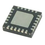
Lead-Free 4 mm 24-Lead PQFN Package
RoHS* Compliant
P/S
Description
The MAPS-010146 is a GaAs pHEMT 4-bit digital
phase shifter with an integrated CMOS driver in a
4 mm PQFN plastic surface mount package. Step
size is 22.5° providing phase shift from 0° to 360° in
22.5° steps. This design has been optimized to
minimize variation in attenuation over the phase shift
range.
The MAPS-010146 is ideally suited for use where
high phase accuracy with minimum loss variation
over the phase shift range are required. The 4 mm
PQFN package provides a smaller footprint than is
typically available for a digital phase shifter with an
internal driver. Typical applications include
communications antennas and phased array radars.
Pin Configuration 2
Pin No.
Function
Pin No.
Function
1
VEE
13
GND
2
P/S
14
RF OUT
3
GND
15
GND
4
GND
16
GND
5
RF IN
17
SER OUT
6
GND
18
VCC
7
GND
19
D6
8
GND
20
D5
9
GND
21
D4
10
GND
22
D3 or LE
11
GND
23
D2 or CLK
12
GND
24
D1 or SER IN
Ordering Information 1
Part Number
Package
MAPS-010146-TR0500
500 piece reel
MAPS-010146-001SMB
Sample Test Board
1. Reference Application Note M513 for reel size information.
2. The exposed pad centered on the package bottom must be
connected to RF and DC ground.
* Restrictions on Hazardous Substances, European Union Directive 2002/95/EC.
1
M/A-COM Technology Solutions Inc. (MACOM) and its affiliates reserve the right to make changes to the product(s) or information contained herein without notice.
Visit www.macom.com for additional data sheets and product information.
For further information and support please visit:
https://www.macom.com/support
�MAPS-010146
Digital Phase Shifter
4-Bit, 8.0 - 12.0 GHz
Rev. V3
Electrical Specifications:
Freq. = 8.0 - 12.0 GHz, TA = 25°C, Z0 = 50 Ω, VCC = +5.0 V, VEE = -5.0 V
Parameter
Test Conditions
Units
Min.
Typ.
Max.
Operating Power 3
8.0 - 12.0 GHz
dBm
—
—
+25
Insertion Loss
(Any Phase State)
Any Phase State
dB
—
6.5
8.8
Attenuation Variation
Across All Phase States
dB
—
±1
—
RMS Attenuation Error 4
All Values Relative to Insertion Loss at
Reference Phase
dB
—
0.7
—
RMS Phase Error 4
All Values Relative to Reference Phase
deg
—
5
—
Phase Accuracy
Relative to Reference Loss State
22.5 Degree Bit
45 Degree Bit
90 Degree Bit
180 Degree Bit
Sum of All Bits
deg
—
—
—
—
—-
± 2.5
±4
±5
±5
± 10
—
—
—
—
—
VSWR
RF IN
RF OUT
Ratio
—
—
1.8:1
1.8:1
—
—
1 dB Compression
Reference State
dBm
—
25
—
Input IP3
Two-tone inputs up to +5 dBm
dBm
—
40
—
TRISE, TFALL
10% to 90% RF, 90% to 10% RF
ns
—
50
—
VCC
VEE
—
—
V
3.0
-5.5
—
-5.0
5.5
-3.0
VIL
VIH
LOW-level input voltage
HIGH-level input voltage
V
0.0
0.7 x VCC
—
—
0.3 x VCC
VCC
lIN (Input Control Current)
VIN = VCC or GND
µA
—
1
—
VOH
VOL
For serial out; IOH = -100 µA
For serial out; IOL = 100 µA
V
VCC - 0.2
—
—
—
—
0.2
ICC
(Quiescent Supply Current)
Vcntrl = VCC or GND
µA
—
—
2
IEE
VEE min to max
Vin = VIL or VIH
mA
-1.0
-0.1
—
5
3. Maximum operating power is the maximum power where the specifications are guaranteed.
4. RMS is calculated across all 15 amplitude or phase states relative to the amplitude or phase in the 0° phase state at a given frequency.
5. This phase shifter is guaranteed to have monotonic phase shift.
2
M/A-COM Technology Solutions Inc. (MACOM) and its affiliates reserve the right to make changes to the product(s) or information contained herein without notice.
Visit www.macom.com for additional data sheets and product information.
For further information and support please visit:
https://www.macom.com/support
�MAPS-010146
Digital Phase Shifter
4-Bit, 8.0 - 12.0 GHz
Rev. V3
Typical Performance Curves
RFIN Return Loss vs. Frequency (All States)
RFOUT Return Loss vs. Frequency (All States)
0
0
-5
-5
-10
-10
-15
-15
-20
-20
-25
-25
-30
-30
-35
8
9
10
11
12
-35
8
9
Frequency (GHz)
10
11
12
Frequency (GHz)
Mean RMS Phase Error vs. Frequency
Mean RMS Amplitude Error vs. Frequency
10
1.4
1.2
8
1.0
6
0.8
0.6
4
0.4
2
0.2
0
8
9
10
11
12
0.0
8
9
Frequency (GHz)
10
11
12
Frequency (GHz)
Phase Error (degrees) vs. State
Amplitude Error (dB) vs. State
2.0
15
8 GHz
9 GHz
10 GHz
11 GHz
12 GHz
10
8 GHz
9 GHz
10 GHz
11 GHz
12 GHz
1.5
1.0
5
0.5
0.0
0
-0.5
-5
-1.0
-10
-15
-1.5
0
45
90
135
180
225
State (deg)
270
315
360
-2.0
0
45
90
135
180
225
270
315
State
3
M/A-COM Technology Solutions Inc. (MACOM) and its affiliates reserve the right to make changes to the product(s) or information contained herein without notice.
Visit www.macom.com for additional data sheets and product information.
For further information and support please visit:
https://www.macom.com/support
360
�MAPS-010146
Digital Phase Shifter
4-Bit, 8.0 - 12.0 GHz
Rev. V3
Typical Performance Curves
Amplitude Variation vs. Phase State
Phase Shift vs. Frequency (Major States)
-2
0
-3
-45
-90
-4
-135
-5
-180
-6
-225
-7
-270
-8
-315
-9
-360
-10
8
9
10
11
12
-405
8.0
8.5
22.5°
45°
67.5°
Absolute Maximum Ratings 6,7
Parameter
Absolute Maximum
Input Power
8.0 - 12.0 GHz
+27 dBm
VCC
-0.5V ≤ VCC ≤ +7.0V
VEE
-7.0V ≤ VEE ≤ +0.5V
D1-D4, P/S, LE, CLK or
SER IN
-0.5V ≤ VIN ≤ VCC + 0.5V
SER OUT
-0.5V ≤ VOUT ≤ VCC + 0.5V
Operating Temperature
-40ºC to +85ºC
Storage Temperature
-65ºC to +150ºC
9.0
9.5
10.0
10.5
11.0
11.5
12.0
Frequency (GHz)
Frequency (GHz)
90°
112.5°
135°
157.5°
180°
205.5°
225°
247.5°
270°
292.5°
315°
337.5°
Sample Board Header Pin Labels
6. Exceeding any one or combination of these limits may cause
permanent damage to this device.
7. M/A-COM Technology Solutions does not recommend
sustained operation near these survivability limits.
Handling Procedures
Please observe the following precautions to avoid damage:
Static Sensitivity
Gallium Arsenide and Silicon Integrated Circuits are sensitive to electrostatic discharge (ESD) and can be
damaged by static electricity. Proper ESD control techniques should be used when handling these devices.
4
M/A-COM Technology Solutions Inc. (MACOM) and its affiliates reserve the right to make changes to the product(s) or information contained herein without notice.
Visit www.macom.com for additional data sheets and product information.
For further information and support please visit:
https://www.macom.com/support
�MAPS-010146
Digital Phase Shifter
4-Bit, 8.0 - 12.0 GHz
Rev. V3
Modes of Operation:
Serial and Direct Parallel
Mode Truth Table 8,9
Serial Mode
The serial control interface (SERIN, CLK, LE,
SEROUT) is compatible with the SPI protocol. SPI
mode is activated when P/S is kept high. The 6-bit
serial word must be loaded with the MSB first. After
shifting in the 6 bit word, a rising edge on LE will set
the phase shifter to the desired state. While LE is
high the CLK is masked to protect the data while
implementing the change. SEROUT is SERIN
delayed by 6 clock cycles.
When P/S is low, the serial control interface is
disabled. When P/S is set high, Pins 22, 23, and 24
have the LE, CLK, and SER IN function.
P/S
LE
Mode
1
X
Serial
0
N/A
Direct Parallel
8. There are two dummy bits (D1 & D2), that must be sent in the
serial mode. This is because the 4 bit phase shifter uses the
same driver as the 6 bit phase shifter.
9. In the parallel mode, D1 and D2 should be tied to ground or to
VCC.
Truth Table (Digital Phase Shifter) 10
D6
D5
D4
D3
D2
D1
Phase Shift
0
0
0
0
X
X
Reference Phase
0
0
0
1
X
X
22.5 deg
0
0
1
0
X
X
45 deg
0
1
0
0
X
X
90 deg
Direct Parallel Mode
1
0
0
0
X
X
180 deg
The parallel mode is enabled when P/S is set low. In
the direct parallel mode, the phase shifter is
controlled by the parallel control inputs directly.
When P/S is set low, Pins 22, 23, and 24 have the
D3, D2, and D1 function.
1
1
1
1
X
X
337.5 deg
In serial mode operation, the outputs will stay
constant while LE is kept low.
10. 0 = CMOS Low; 1 = CMOS High, X is CMOS Low or High
Serial Interface Timing Characteristics
Symbol
Parameter
tSCK
Typical Performance
Units
-40°C
25°C
+85°C
Min. Serial Clock Period
100
100
100
ns
tCS
Min. Control Set-up Time
20
20
20
ns
tCH
Min. Control Hold Time
20
20
20
ns
tLS
Min. LE Set-up Time
10
10
10
ns
tLEW
Min. LE Pulse Width
10
10
10
ns
tLH
Min. Serial Clock Hold Time from LE
10
10
10
ns
tLES
Min. LE Pulse Spacing
630
630
630
ns
5
M/A-COM Technology Solutions Inc. (MACOM) and its affiliates reserve the right to make changes to the product(s) or information contained herein without notice.
Visit www.macom.com for additional data sheets and product information.
For further information and support please visit:
https://www.macom.com/support
�MAPS-010146
Digital Phase Shifter
4-Bit, 8.0 - 12.0 GHz
Rev. V3
Functionality
Modes of Operation: Serial and Direct Parallel
Serial Input Interface Timing Diagram
tLS
tLEW
tLH
SERIAL
CLK
LE
tLES
CONTROL
WORD
D5
MSB
tCS
D4
D1
D0
LSB
tCH
Lead Free 4 mm 24-Lead PQFN †
†
Reference Application Note S2083 for lead-free solder reflow recommendations.
Meets JEDEC moisture sensitivity level 1 requirements.
Plating is 100% matte tin over copper.
6
M/A-COM Technology Solutions Inc. (MACOM) and its affiliates reserve the right to make changes to the product(s) or information contained herein without notice.
Visit www.macom.com for additional data sheets and product information.
For further information and support please visit:
https://www.macom.com/support
�MAPS-010146
Digital Phase Shifter
4-Bit, 8.0 - 12.0 GHz
Rev. V3
M/A-COM Technology Solutions Inc. All rights reserved.
Information in this document is provided in connection with M/A-COM Technology Solutions Inc ("MACOM")
products. These materials are provided by MACOM as a service to its customers and may be used for
informational purposes only. Except as provided in MACOM's Terms and Conditions of Sale for such products or
in any separate agreement related to this document, MACOM assumes no liability whatsoever. MACOM
assumes no responsibility for errors or omissions in these materials. MACOM may make changes to
specifications and product descriptions at any time, without notice. MACOM makes no commitment to update
the information and shall have no responsibility whatsoever for conflicts or incompatibilities arising from future
changes to its specifications and product descriptions. No license, express or implied, by estoppels or otherwise,
to any intellectual property rights is granted by this document.
THESE MATERIALS ARE PROVIDED "AS IS" WITHOUT WARRANTY OF ANY KIND, EITHER EXPRESS OR
IMPLIED, RELATING TO SALE AND/OR USE OF MACOM PRODUCTS INCLUDING LIABILITY OR
WARRANTIES RELATING TO FITNESS FOR A PARTICULAR PURPOSE, CONSEQUENTIAL OR
INCIDENTAL DAMAGES, MERCHANTABILITY, OR INFRINGEMENT OF ANY PATENT, COPYRIGHT OR
OTHER INTELLECTUAL PROPERTY RIGHT. MACOM FURTHER DOES NOT WARRANT THE ACCURACY
OR COMPLETENESS OF THE INFORMATION, TEXT, GRAPHICS OR OTHER ITEMS CONTAINED WITHIN
THESE MATERIALS. MACOM SHALL NOT BE LIABLE FOR ANY SPECIAL, INDIRECT, INCIDENTAL, OR
CONSEQUENTIAL DAMAGES, INCLUDING WITHOUT LIMITATION, LOST REVENUES OR LOST PROFITS,
WHICH MAY RESULT FROM THE USE OF THESE MATERIALS.
MACOM products are not intended for use in medical, lifesaving or life sustaining applications. MACOM
customers using or selling MACOM products for use in such applications do so at their own risk and agree to
fully indemnify MACOM for any damages resulting from such improper use or sale.
7
M/A-COM Technology Solutions Inc. (MACOM) and its affiliates reserve the right to make changes to the product(s) or information contained herein without notice.
Visit www.macom.com for additional data sheets and product information.
For further information and support please visit:
https://www.macom.com/support
�