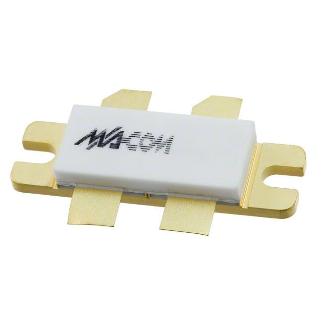
MRF175GU
The RF MOSFET Line
200/150W, 500MHz, 28V
Designed for broadband commercial and military applications using push
pull circuits at frequencies to 500 MHz. The high power, high gain and
broadband performance of these devices makes possible solid state
transmitters for FM broadcast or TV channel frequency bands.
Rev. V1
Product Image
N–Channel enhancement mode
Guaranteed performance
MRF175GV @ 28 V, 225 MHz (―V‖ Suffix)
Output power — 200 W
Power gain — 14 dB typ
Efficiency — 65% typ`
100% ruggedness tested at rated output power
Low thermal resistance
Low Crss — 20 pF typ @ VDS = 28 V
CASE 375–04, STYLE 2
1
M/A-COM Technology Solutions Inc. (MACOM) and its affiliates reserve the right to make changes to the product(s) or information contained herein without notice.
Visit www.macom.com for additional data sheets and product information.
For further information and support please visit:
https://www.macom.com/support
�MRF175GU
The RF MOSFET Line
200/150W, 500MHz, 28V
Rev. V1
2
M/A-COM Technology Solutions Inc. (MACOM) and its affiliates reserve the right to make changes to the product(s) or information contained herein without notice.
Visit www.macom.com for additional data sheets and product information.
For further information and support please visit:
https://www.macom.com/support
�MRF175GU
The RF MOSFET Line
200/150W, 500MHz, 28V
Rev. V1
3
M/A-COM Technology Solutions Inc. (MACOM) and its affiliates reserve the right to make changes to the product(s) or information contained herein without notice.
Visit www.macom.com for additional data sheets and product information.
For further information and support please visit:
https://www.macom.com/support
�MRF175GU
The RF MOSFET Line
200/150W, 500MHz, 28V
Rev. V1
4
M/A-COM Technology Solutions Inc. (MACOM) and its affiliates reserve the right to make changes to the product(s) or information contained herein without notice.
Visit www.macom.com for additional data sheets and product information.
For further information and support please visit:
https://www.macom.com/support
�MRF175GU
The RF MOSFET Line
200/150W, 500MHz, 28V
Rev. V1
5
M/A-COM Technology Solutions Inc. (MACOM) and its affiliates reserve the right to make changes to the product(s) or information contained herein without notice.
Visit www.macom.com for additional data sheets and product information.
For further information and support please visit:
https://www.macom.com/support
�MRF175GU
The RF MOSFET Line
200/150W, 500MHz, 28V
Rev. V1
6
M/A-COM Technology Solutions Inc. (MACOM) and its affiliates reserve the right to make changes to the product(s) or information contained herein without notice.
Visit www.macom.com for additional data sheets and product information.
For further information and support please visit:
https://www.macom.com/support
�MRF175GU
The RF MOSFET Line
200/150W, 500MHz, 28V
Rev. V1
7
M/A-COM Technology Solutions Inc. (MACOM) and its affiliates reserve the right to make changes to the product(s) or information contained herein without notice.
Visit www.macom.com for additional data sheets and product information.
For further information and support please visit:
https://www.macom.com/support
�MRF175GU
The RF MOSFET Line
200/150W, 500MHz, 28V
Rev. V1
8
M/A-COM Technology Solutions Inc. (MACOM) and its affiliates reserve the right to make changes to the product(s) or information contained herein without notice.
Visit www.macom.com for additional data sheets and product information.
For further information and support please visit:
https://www.macom.com/support
�MRF175GU
The RF MOSFET Line
200/150W, 500MHz, 28V
Rev. V1
9
M/A-COM Technology Solutions Inc. (MACOM) and its affiliates reserve the right to make changes to the product(s) or information contained herein without notice.
Visit www.macom.com for additional data sheets and product information.
For further information and support please visit:
https://www.macom.com/support
�MRF175GU
The RF MOSFET Line
200/150W, 500MHz, 28V
Rev. V1
10
M/A-COM Technology Solutions Inc. (MACOM) and its affiliates reserve the right to make changes to the product(s) or information contained herein without notice.
Visit www.macom.com for additional data sheets and product information.
For further information and support please visit:
https://www.macom.com/support
�MRF175GU
The RF MOSFET Line
200/150W, 500MHz, 28V
Rev. V1
11
M/A-COM Technology Solutions Inc. (MACOM) and its affiliates reserve the right to make changes to the product(s) or information contained herein without notice.
Visit www.macom.com for additional data sheets and product information.
For further information and support please visit:
https://www.macom.com/support
�MRF175GU
The RF MOSFET Line
200/150W, 500MHz, 28V
Rev. V1
12
M/A-COM Technology Solutions Inc. (MACOM) and its affiliates reserve the right to make changes to the product(s) or information contained herein without notice.
Visit www.macom.com for additional data sheets and product information.
For further information and support please visit:
https://www.macom.com/support
�MRF175GU
The RF MOSFET Line
200/150W, 500MHz, 28V
Rev. V1
13
M/A-COM Technology Solutions Inc. (MACOM) and its affiliates reserve the right to make changes to the product(s) or information contained herein without notice.
Visit www.macom.com for additional data sheets and product information.
For further information and support please visit:
https://www.macom.com/support
�MRF175GU
The RF MOSFET Line
200/150W, 500MHz, 28V
Rev. V1
RF POWER MOSFET CONSIDERATIONS
MOSFET CAPACITANCES
The physical structure of a MOSFET results in capacitors
between the terminals. The metal oxide gate structure determines the capacitors from gate–to–drain (Cgd), and gate–
to–source (Cgs). The PN junction formed during the fabrication of the MOSFET results in a junction capacitance from
drain–to–source (Cds).
These capacitances are characterized as input (C iss), output (Coss) and reverse transfer (Crss) capacitances on data
sheets. The relationships between the inter–terminal capacitances and those given on data sheets are shown below. The Ciss can be specified in two ways:
1.
2.
Drain shorted to source and positive voltage at the
gate.
Positive voltage of the drain in respect to source and
zerovolts at the gate. In the latter case the numbers are
lower. However, neither method represents the actual
operating conditions in RF applications.
The Ciss givenin the electrical characteristics table was
measured using method 2 above. It should be noted that
Ciss, Coss, Crss are measured at zero drain current and are
provided for general information about the device. They are
not RF design parameters and no attempt should be made
to use them as such.
under specific test conditions for gate–source voltage and
drain
current. For MOSFETs, VDS(on) has a positive temperature
coefficient and constitutes an important design consideration
at high temperatures, because it contributes to the power
dissipation within the device.
GATE CHARACTERISTICS
The gate of the MOSFET is a polysilicon material, and is
electrically isolated from the source by a layer of oxide. The
input resistance is very high — on the order of 109 ohms —
resulting in a leakage current of a few nanoamperes.
Gate control is achieved by applying a positive voltage
slightly in excess of the gate–to–source threshold voltage,
VGS(th).
Gate Voltage Rating — Never exceed the gate voltage rating (or any of the maximum ratings on the front page). Exceeding the rated VGS can result in permanent damage to
the oxide layer in the gate region.
Gate Termination — The gates of this device are essentially capacitors. Circuits that leave the gate open–circuited
or floating should be avoided. These conditions can result in
turn–on of the devices due to voltage build–up on the input
capacitor due to leakage currents or pickup.
Gate Protection — These devices do not have an internal
monolithic zener diode from gate–to–source. If gate protection is required, an external zener diode is recommended.
Using a resistor to keep the gate–to–source impedance
low also helps damp transients and serves another important
function. Voltage transients on the drain can be coupled to
the gate through the parasitic gate–drain capacitance. If the
gate–to–source impedance and the rate of voltage change
on the drain are both high, then the signal coupled to the
gate may be large enough to exceed the gate–threshold
voltage and turn the device on.
LINEARITY AND GAIN CHARACTERISTICS
In addition to the typical IMD and power gain, data presented in Figure 3 may give the designer additional information on the capabilities of this device. The graph represents the small signal unity current gain frequency at a
given drain current level. This is equivalent to fT for bipolar
transistors. Since this test is performed at a fast sweep
speed, heating of the device does not occur. Thus, in normal use, the highertemperatures may degrade these characteristics to some extent.
HANDLING CONSIDERATIONS
When shipping, the devices should be transported only in
antistatic bags or conductive foam. Upon removal from the
packaging, careful handling procedures should be adhered
to. Those handling the devices should wear grounding
straps and devices not in the antistatic packaging should be
kept in metal tote bins. MOSFETs should be handled by the
case and not by the leads, and when testing the device, all
leads should make good electrical contact before voltage is
applied. As a final note, when placing the FET into the system it is designed for, soldering should be done with
grounded equipment.
DRAIN CHARACTERISTICS
One figure of merit for a FET is its static resistance in the
full–on condition. This on–resistance, VDS(on), occurs in the
linear region of the output characteristic and is specified
DESIGN CONSIDERATIONS
The MRF175G is a RF power N–channel enhancement
mode field–effect transistor (FETs) designed for HF, VHF
and
14
M/A-COM Technology Solutions Inc. (MACOM) and its affiliates reserve the right to make changes to the product(s) or information contained herein without notice.
Visit www.macom.com for additional data sheets and product information.
For further information and support please visit:
https://www.macom.com/support
�MRF175GU
The RF MOSFET Line
200/150W, 500MHz, 28V
Rev. V1
RF POWER MOSFET CONSIDERATIONS
MOSFET CAPACITANCES
The physical structure of a MOSFET results in capacitors
between the terminals. The metal oxide gate structure determines the capacitors from gate–to–drain (Cgd), and gate–
to–source (Cgs). The PN junction formed during the fabrication of the MOSFET results in a junction capacitance from
drain–to–source (Cds).
These capacitances are characterized as input (C iss),
output (Coss) and reverse transfer (Crss) capacitances on
data sheets. The relationships between the inter–terminal
capacitances and those given on data sheets are shown
below. The Ciss can be specified in two ways:
1.
Drain shorted to source and positive voltage at the
gate.
2.
Positive voltage of the drain in respect to source
and zerovolts at the gate. In the latter case the
numbers are lower. However, neither method
represents the actual operating conditions in RF
applications.
The Ciss givenin the electrical characteristics table was
measured using method 2 above. It should be noted thatCiss, Coss, Crss are measured at zero drain current and are
provided for general information about the device. They are
not RF design parameters and no attempt should be made
to use them as such.
LINEARITY AND GAIN CHARACTERISTICS
In addition to the typical IMD and power gain, data presented in Figure 3 may give the designer additional information on the capabilities of this device. The graph represents the small signal unity current gain frequency at a
given drain current level. This is equivalent to fT for bipolar
transistors. Since this test is performed at a fast sweep
speed, heating of the device does not occur. Thus, in normal use, the higher temperatures may degrade these characteristics to some extent.
DRAIN CHARACTERISTICS
One figure of merit for a FET is its static resistance in the
full–on condition. This on–resistance, VDS(on), occurs in the
linear region of the output characteristic and is specified under specific test conditions for gate–source voltage and drain
current. For MOSFETs, VDS(on) has a positive temperature
coefficient and constitutes an important design consideration
at high temperatures, because it contributes to the power
dissipation within the device.
GATE CHARACTERISTICS
The gate of the MOSFET is a polysilicon material, and is
electrically isolated from the source by a layer of oxide. The
input resistance is very high — on the order of 109 ohms —
resulting in a leakage current of a few nanoamperes. Gate
control is achieved by applying a positive voltage slightly in
excess of the gate–to–source threshold voltage, VGS(th).
Gate Voltage Rating — Never exceed the gate voltage rating (or any of the maximum ratings on the front page). Exceeding the rated VGS can result in permanent damage to
the oxide layer in the gate region.
Gate Termination — The gates of this device are essentially capacitors. Circuits that leave the gate open–circuited
or floating should be avoided. These conditions can result in
turn–on of the devices due to voltage build–up on the input
capacitor due to leakage currents or pickup.
Gate Protection — These devices do not have an internal
monolithic zener diode from gate–to–source. If gate protection is required, an external zener diode is recommended.
Using a resistor to keep the gate–to–source impedance low
also helps damp transients and serves another important
function. Voltage transients on the drain can be coupled to
the gate through the parasitic gate–drain capacitance. If the
gate–to–source impedance and the rate of voltage change
on the drain are both high, then the signal coupled to the
gate may be large enough to exceed the gate–threshold
voltage and turn the device on.
HANDLING CONSIDERATIONS
When shipping, the devices should be transported only in
antistatic bags or conductive foam. Upon removal from the
packaging, careful handling procedures should be adhered
to. Those handling the devices should wear grounding
straps and devices not in the antistatic packaging should be
kept in metal tote bins. MOSFETs should be handled by the
case and not by the leads, and when testing the device, all
leads should make good electrical contact before voltage is
applied. As a final note, when placing the FET into the system it is designed for, soldering should be done with
grounded equipment.
DESIGN CONSIDERATIONS
The MRF175G is a RF power N–channel enhancement
mode field–effect transistor (FETs) designed for HF, VHF
andUHF power amplifier applications. M/A-COM RF MOSFETs feature a vertical structure with a planar design. M/A-
15
M/A-COM Technology Solutions Inc. (MACOM) and its affiliates reserve the right to make changes to the product(s) or information contained herein without notice.
Visit www.macom.com for additional data sheets and product information.
For further information and support please visit:
https://www.macom.com/support
�MRF175GU
The RF MOSFET Line
200/150W, 500MHz, 28V
COM Application Note AN211A, FETs in Theory and Practice, is suggested reading for those not familiar with the construction and characteristics of FETs.
The major advantages of RF power FETs include high
gain, low noise, simple bias systems, relative immunity from
thermal runaway, and the ability to withstand severely mismatched loads without suffering damage. Power output can
be varied over a wide range with a low power dc control signal.
DC BIAS
The MRF175G is an enhancement mode FET and, therefore, does not conduct when drain voltage is applied. Drain
current flows when a positive voltage is applied to the gate.
Rev. V1
RF power FETs require forward bias for optimum performance. The value of quiescent drain current (IDQ) is not critical
for many applications. The MRF175G was characterized
at IDQ = 100 mA, each side, which is the suggested minimumvalue of IDQ. For special applications such as linear
amplification, IDQ may have to be selected to optimize the
critical parameters. The gate is a dc open circuit and draws
no current. Therefore, the gate bias circuit may be just a
simple resistive divider network. Some applications may
require a more elaborate bias sytem.
GAIN CONTROL
Power output of the MRF175G may be controlled from its
rated value down to zero (negative gain) by varying the dc
gate voltage. This feature facilitates the design of manual
gain control, AGC/ALC and modulation systems.
16
M/A-COM Technology Solutions Inc. (MACOM) and its affiliates reserve the right to make changes to the product(s) or information contained herein without notice.
Visit www.macom.com for additional data sheets and product information.
For further information and support please visit:
https://www.macom.com/support
�MRF175GU
The RF MOSFET Line
200/150W, 500MHz, 28V
Rev. V1
M/A-COM Technology Solutions Inc. All rights reserved.
Information in this document is provided in connection with M/A-COM Technology Solutions Inc ("MACOM")
products. These materials are provided by MACOM as a service to its customers and may be used for
informational purposes only. Except as provided in MACOM's Terms and Conditions of Sale for such products or
in any separate agreement related to this document, MACOM assumes no liability whatsoever. MACOM
assumes no responsibility for errors or omissions in these materials. MACOM may make changes to
specifications and product descriptions at any time, without notice. MACOM makes no commitment to update
the information and shall have no responsibility whatsoever for conflicts or incompatibilities arising from future
changes to its specifications and product descriptions. No license, express or implied, by estoppels or otherwise,
to any intellectual property rights is granted by this document.
THESE MATERIALS ARE PROVIDED "AS IS" WITHOUT WARRANTY OF ANY KIND, EITHER EXPRESS OR
IMPLIED, RELATING TO SALE AND/OR USE OF MACOM PRODUCTS INCLUDING LIABILITY OR
WARRANTIES RELATING TO FITNESS FOR A PARTICULAR PURPOSE, CONSEQUENTIAL OR
INCIDENTAL DAMAGES, MERCHANTABILITY, OR INFRINGEMENT OF ANY PATENT, COPYRIGHT OR
OTHER INTELLECTUAL PROPERTY RIGHT. MACOM FURTHER DOES NOT WARRANT THE ACCURACY
OR COMPLETENESS OF THE INFORMATION, TEXT, GRAPHICS OR OTHER ITEMS CONTAINED WITHIN
THESE MATERIALS. MACOM SHALL NOT BE LIABLE FOR ANY SPECIAL, INDIRECT, INCIDENTAL, OR
CONSEQUENTIAL DAMAGES, INCLUDING WITHOUT LIMITATION, LOST REVENUES OR LOST PROFITS,
WHICH MAY RESULT FROM THE USE OF THESE MATERIALS.
MACOM products are not intended for use in medical, lifesaving or life sustaining applications. MACOM
customers using or selling MACOM products for use in such applications do so at their own risk and agree to
fully indemnify MACOM for any damages resulting from such improper use or sale.
17
M/A-COM Technology Solutions Inc. (MACOM) and its affiliates reserve the right to make changes to the product(s) or information contained herein without notice.
Visit www.macom.com for additional data sheets and product information.
For further information and support please visit:
https://www.macom.com/support
�