XP1027-BD
Power Amplifier
27.0-31.0 GHz
Rev. V1
Features
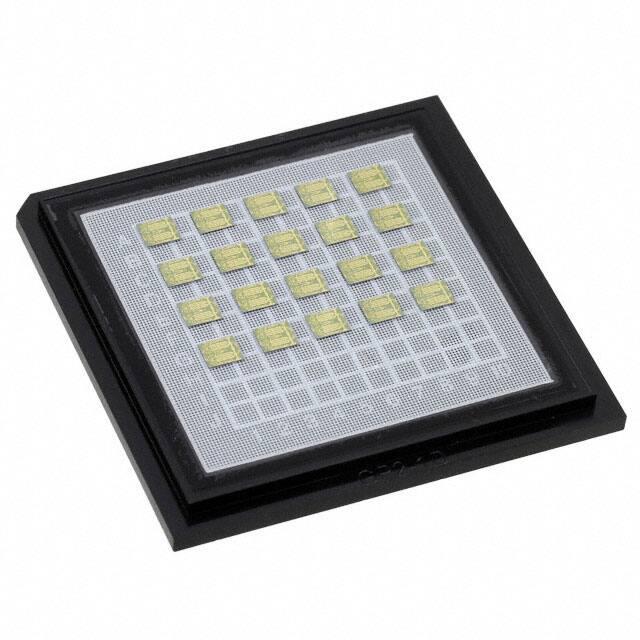
Chip Device Layout
Ka-Band 4 W Power Amplifier
Balanced Design Provides Good Input/Output
Match
21.0 dB Small Signal Gain
+35.5 dBm Saturated Output Power
+43.0 dBm Output Third Order Intercept (OIP3)
100% On-Wafer RF, DC and Output Power
Testing
100% Visual Inspection to MIL-STD-883 Method
2010
RoHS* Compliant and 260°C Reflow Compatible
Description
M/A-COM Tech’s three stage 27.0-31.0 GHz GaAs
MMIC power amplifier has a small signal gain of
21.0 dB with +35.5 dBm saturated output power.
The device also includes Lange couplers to achieve
good input/output return loss. This MMIC uses M/ACOM Tech’s GaAs PHEMT device model
technology, and is based upon electron beam
lithography to ensure high repeatability and
uniformity. The chip has surface passivation to
protect and provide a rugged part with backside via
holes and gold metallization to allow either a
conductive epoxy or eutectic solder die attach
process. This device is well suited for Millimeterwave Point-to-Point Radio, LMDS, SATCOM and
VSAT applications.
Absolute Maximum Ratings
Parameter
Absolute Max.
Supply Voltage (Vd)
+6.0 VDC2
Supply Current (Id1,2,3)
325,825,1575 mA
Gate Bias Voltage (Vg)
+0.3 VDC
Input Power (Pin)
+25 dBm
Storage Temperature (Tstg)
-65 °C to +165 °C
Operating Temperature (Ta)
-55 °C to +85 °C
Channel Temperature (Tch)1
175 °C
1. Channel temperature directly affects a device's MTTF. Channel temperature should be kept as low as possible to maximize
lifetime.
2. Under pulsed bias conditions, under CW Psat conditions further reduction in max supply voltage (~0.5V) is recommended.
Ordering Information
Part Number
Package
XP1027-BD-000V
“V” - vacuum release
gel paks
XP1027-BD-EV1
evaluation module
1
ADVANCED: Data Sheets contain information regarding a product M/A-COM Technology Solutions
• North America Tel: 800.366.2266 • Europe Tel: +353.21.244.6400
is considering for development. Performance is based on target specifications, simulated results,
• India Tel: +91.80.43537383
• China Tel: +86.21.2407.1588
and/or prototype measurements. Commitment to develop is not guaranteed.
Visit www.macomtech.com for additional data sheets and product information.
PRELIMINARY: Data Sheets contain information regarding a product M/A-COM Technology
Solutions has under development. Performance is based on engineering tests. Specifications are
typical. Mechanical outline has been fixed. Engineering samples and/or test data may be available. M/A-COM Technology Solutions Inc. and its affiliates reserve the right to make
Commitment to produce in volume is not guaranteed.
changes to the product(s) or information contained herein without notice.
�XP1027-BD
Power Amplifier
27.0-31.0 GHz
Rev. V1
Electrical Specifications: 27-31 GHz (Ambient Temperature T = 25°C)
Parameter
Units
Min.
Typ.
Max.
Input Return Loss (S11)
dB
-
20.0
-
Output Return Loss (S22)
dB
-
20.0
-
Small Signal Gain (S21)1
dB
-
21.0
-
Gain Flatness (S21)
dB
-
+/-1.0
-
Reverse Isolation (S12)
dB
-
50.0
-
Output Power for 1 dB Compression (P1dB)
dBm
-
+34.5
-
Output Third Order Intercept Point (OIP3)
dBm
-
+43.0
-
Saturated Output Power (Psat)1
dBm
-
+35.5
-
Drain Bias Voltage (Vd1,2,3)
VDC
-
+5.5
+5.8
Gate Bias Voltage (Vg1,2,3)
VDC
-1.0
-0.7
0.0
Supply Current (Id1) (Vd=5.5 V, Vg=-0.7 V Typical)
mA
-
250
300
Supply Current (Id2) (Vd=5.5 V, Vg=-0.7 V Typical)
mA
-
625
750
Supply Current (Id3) (Vd=5.5 V, Vg=-0.7 V Typical)
mA
-
1185
1435
1. Measured on wafer pulsed
2
ADVANCED: Data Sheets contain information regarding a product M/A-COM Technology Solutions
• North America Tel: 800.366.2266 • Europe Tel: +353.21.244.6400
is considering for development. Performance is based on target specifications, simulated results,
• India Tel: +91.80.43537383
• China Tel: +86.21.2407.1588
and/or prototype measurements. Commitment to develop is not guaranteed.
Visit www.macomtech.com for additional data sheets and product information.
PRELIMINARY: Data Sheets contain information regarding a product M/A-COM Technology
Solutions has under development. Performance is based on engineering tests. Specifications are
typical. Mechanical outline has been fixed. Engineering samples and/or test data may be available. M/A-COM Technology Solutions Inc. and its affiliates reserve the right to make
Commitment to produce in volume is not guaranteed.
changes to the product(s) or information contained herein without notice.
�XP1027-BD
Power Amplifier
27.0-31.0 GHz
Rev. V1
Typical Performance Curves (On-Wafer1)
30
26
20
25
10
24
0
23
-10
22
-20
-30
21
-40
20
-50
19
-60
-70
18
-80
17
16
25.0
-90
26.0
27.0
28.0
29.0
30.0
31.0
32.0
33.0
-100
20.0
0
0
-5
-5
-10
-10
-15
-15
-20
-20
-25
-25
-30
-30
-35
-35
-40
25.0
26.0
27.0
28.0
29.0
30.0
31.0
32.0
33.0
-40
20.0
0
0
-5
-5
-10
-10
-15
-15
-20
-20
-25
-25
-30
-30
-35
-35
-40
-40
-45
-45
-50
25.0
26.0
27.0
28.0
29.0
30.0
31.0
32.0
33.0
22.0
24.0
26.0
28.0
30.0
32.0
34.0
36.0
38.0
40.0
22.0
24.0
26.0
28.0
30.0
32.0
34.0
36.0
38.0
40.0
22.0
24.0
26.0
28.0
30.0
32.0
34.0
36.0
38.0
40.0
-50
20.0
1. Measurements – On-Wafer S-Parameters have been taken using reduced bias conditions as shown. Measurements are referenced 150
um in from RF In/Out pad edge. For optimum performance M/A-COM Tech T-pad transition and tuned output matching network is recommended. For additional information see the M/A-COM Tech “T-Pad Transition” application note. Contact technical sales for output matching
network information.
3
ADVANCED: Data Sheets contain information regarding a product M/A-COM Technology Solutions
• North America Tel: 800.366.2266 • Europe Tel: +353.21.244.6400
is considering for development. Performance is based on target specifications, simulated results,
• India Tel: +91.80.43537383
• China Tel: +86.21.2407.1588
and/or prototype measurements. Commitment to develop is not guaranteed.
Visit www.macomtech.com for additional data sheets and product information.
PRELIMINARY: Data Sheets contain information regarding a product M/A-COM Technology
Solutions has under development. Performance is based on engineering tests. Specifications are
typical. Mechanical outline has been fixed. Engineering samples and/or test data may be available. M/A-COM Technology Solutions Inc. and its affiliates reserve the right to make
Commitment to produce in volume is not guaranteed.
changes to the product(s) or information contained herein without notice.
�XP1027-BD
Power Amplifier
27.0-31.0 GHz
Rev. V1
Typical Performance Curves (On-Wafer1) (cont.)
26
24
22
20
18
16
14
12
40
39
38
37
36
35
10
8
6
4
34
33
32
2
0
31
30
27.0
28.0
29.0
30.0
31.0
32.0
33.0
22
23
24
28 GHz
25
26
27
29 GHz
28
29
30
30 GHz
31
32
31 GHz
33
34
35
36
37
32 GHz
2000
1800
1600
1400
1200
1000
800
600
400
200
0
22
23
24
25
26
27
28
Id1
29
30
Id2
31
32
33
34
35
36
37
Id3
1. Measurements – On-Wafer Output Power data has been taken using bias conditions as shown. Measurements are referenced 150 um in
from RF In/Out pad edge. For optimum performance M/A-COM Tech T-pad transition and tuned output matching network is recommended.
For additional information see the M/A-COM Tech “T-Pad Transition” application note. Contact technical sales for output matching network
information.
4
ADVANCED: Data Sheets contain information regarding a product M/A-COM Technology Solutions
• North America Tel: 800.366.2266 • Europe Tel: +353.21.244.6400
is considering for development. Performance is based on target specifications, simulated results,
• India Tel: +91.80.43537383
• China Tel: +86.21.2407.1588
and/or prototype measurements. Commitment to develop is not guaranteed.
Visit www.macomtech.com for additional data sheets and product information.
PRELIMINARY: Data Sheets contain information regarding a product M/A-COM Technology
Solutions has under development. Performance is based on engineering tests. Specifications are
typical. Mechanical outline has been fixed. Engineering samples and/or test data may be available. M/A-COM Technology Solutions Inc. and its affiliates reserve the right to make
Commitment to produce in volume is not guaranteed.
changes to the product(s) or information contained herein without notice.
�XP1027-BD
Power Amplifier
27.0-31.0 GHz
Rev. V1
Typical Performance Curves (On-Wafer1) (cont.)
40
40
39
39
38
38
37
37
36
36
35
35
34
34
33
33
32
32
31
31
30
27.0
28.0
29.0
30.0
31.0
32.0
33.0
30
27.0
28.0
40
40
Vg=-1.0V, Id=1196 mA
Vg=-0.9V, Id=1491 mA
Vg=-0.8V, Id=1683 mA
Vg=-0.7V, Id=1944 mA
Vg=-0.6V, Id=2318 mA
35
30
30
25
20
20
15
15
10
10
5
5
0
18
20
22
24
26
28
30
32
34
36
38
30.0
31.0
32.0
33.0
Vg=-1.0 V, Id=1346 mA
Vg=-0.9V, Id=1496 mA
Vg=-0.8V, Id=1795 mA
Vg=-0.7V, Id=2019 mA
Vg=-0.6V, Id=2468 mA
35
25
29.0
0
18
20
22
24
26
28
30
32
34
36
38
1. Measurements – On-Wafer Output Power data has been taken using bias conditions as shown. Measurements are referenced 150 um in
from RF In/Out pad edge. For optimum performance M/A-COM Tech T-pad transition and tuned output matching network is recommended.
For additional information see the M/A-COM Tech “T-Pad Transition” application note. Contact technical sales for output matching network
information.
5
ADVANCED: Data Sheets contain information regarding a product M/A-COM Technology Solutions
• North America Tel: 800.366.2266 • Europe Tel: +353.21.244.6400
is considering for development. Performance is based on target specifications, simulated results,
• India Tel: +91.80.43537383
• China Tel: +86.21.2407.1588
and/or prototype measurements. Commitment to develop is not guaranteed.
Visit www.macomtech.com for additional data sheets and product information.
PRELIMINARY: Data Sheets contain information regarding a product M/A-COM Technology
Solutions has under development. Performance is based on engineering tests. Specifications are
typical. Mechanical outline has been fixed. Engineering samples and/or test data may be available. M/A-COM Technology Solutions Inc. and its affiliates reserve the right to make
Commitment to produce in volume is not guaranteed.
changes to the product(s) or information contained herein without notice.
�XP1027-BD
Power Amplifier
27.0-31.0 GHz
Rev. V1
Typical Performance Curves (On-Wafer1) (cont.)
45
45
44
44
43
43
42
42
41
41
40
40
39
39
38
38
37
37
36
36
35
35
12 13 14 15 16 17 18 19 20 21 22 23 24 25 26 27 28 29 30
28 GHz
29 GHz
30 GHz
31 GHz
32 GHz
12 13 14 15 16 17 18 19 20 21 22 23 24 25 26 27 28 29 30
28 GHz
29 GHz
30 GHz
31 GHz
32 GHz
45
44
43
42
41
40
39
38
37
36
35
12 13 14 15 16 17 18 19 20 21 22 23 24 25 26 27 28 29 30
28 GHz
29 GHz
30 GHz
31 GHz
32 GHz
Additional Data – The XP1027 device consists of a balanced XP1026 pair. See the XP1026 data sheet for additional data concerning OIP3
control and optimization.
1. Measurements – On-Wafer Output Power data has been taken using bias conditions as shown. Measurements are referenced 150 um in
from RF In/Out pad edge. For optimum performance M/A-COM Tech T-pad transition and tuned output matching network is recommended.
For additional information see the M/A-COM Tech “T-Pad Transition” application note. Contact technical sales for output matching network
information.
6
ADVANCED: Data Sheets contain information regarding a product M/A-COM Technology Solutions
• North America Tel: 800.366.2266 • Europe Tel: +353.21.244.6400
is considering for development. Performance is based on target specifications, simulated results,
• India Tel: +91.80.43537383
• China Tel: +86.21.2407.1588
and/or prototype measurements. Commitment to develop is not guaranteed.
Visit www.macomtech.com for additional data sheets and product information.
PRELIMINARY: Data Sheets contain information regarding a product M/A-COM Technology
Solutions has under development. Performance is based on engineering tests. Specifications are
typical. Mechanical outline has been fixed. Engineering samples and/or test data may be available. M/A-COM Technology Solutions Inc. and its affiliates reserve the right to make
Commitment to produce in volume is not guaranteed.
changes to the product(s) or information contained herein without notice.
�XP1027-BD
Power Amplifier
27.0-31.0 GHz
Rev. V1
Typical Performance Curves (Text Fixture1)
28
39
27
38
26
37
25
36
24
35
23
22
34
21
33
20
32
19
31
18
30
17
16
25.0
26.0
27.0
28.0
+85 deg C
29.0
30.0
-40 deg C
31.0
32.0
33.0
29
27.0
27.5
28.0
28.5
29.0
+85 deg C
+25 deg C
0
29.5
30.0
30.5
-40 deg C
31.0
31.5
32.0
32.5
+25 deg C
0
-5
-5
-10
-10
-15
-20
-15
-25
-20
-30
-25
25.0
26.0
27.0
28.0
+85 deg C
29.0
-40 deg C
30.0
31.0
32.0
33.0
-35
25.0
27.0
+25 deg C
28.0
+85 deg C
39
39
38
38
37
29.0
30.0
-40 deg C
31.0
32.0
33.0
+25 deg C
37
36
36
35
35
34
34
33
33
32
31
32
30
31
29
27.0
26.0
30
27.5
28.0
28.5
29.0
29.5
30.0
30.5
31.0
31.5
32.0
32.5
29
27.0
+85 deg C
-40 deg C
27.5
28.0
28.5
29.0
29.5
30.0
30.5
31.0
31.5
32.0
+25 deg C
+ 85 deg C
-40 deg C
+25 deg C
1. Measurements – Test Fixture data includes all bond wire parasitics, uncompensated RF In/Out M/A-COM Tech T-Pad transitions and RF
ceramic circuit losses. For Gain and Output Power curves RF In/Out circuit losses have been removed.
7
ADVANCED: Data Sheets contain information regarding a product M/A-COM Technology Solutions
• North America Tel: 800.366.2266 • Europe Tel: +353.21.244.6400
is considering for development. Performance is based on target specifications, simulated results,
• India Tel: +91.80.43537383
• China Tel: +86.21.2407.1588
and/or prototype measurements. Commitment to develop is not guaranteed.
Visit www.macomtech.com for additional data sheets and product information.
PRELIMINARY: Data Sheets contain information regarding a product M/A-COM Technology
Solutions has under development. Performance is based on engineering tests. Specifications are
typical. Mechanical outline has been fixed. Engineering samples and/or test data may be available. M/A-COM Technology Solutions Inc. and its affiliates reserve the right to make
Commitment to produce in volume is not guaranteed.
changes to the product(s) or information contained herein without notice.
�XP1027-BD
Power Amplifier
27.0-31.0 GHz
Rev. V1
S-Parameters (On-Wafer1)
Typcial S-Parameter Data for XP1027-BD
Vd=5.0 V, Id=1817 mA
Frequency
((GHz))
20.0
21.0
22.0
23.0
24.0
25.0
26.0
27 0
27.0
28.0
29.0
30.0
31.0
32.0
33.0
34.0
35.0
36.0
37.0
38.0
39.0
40.0
S11
( g)
(Mag)
0.095
0.094
0.081
0.056
0.021
0.034
0.075
0 063
0.063
0.033
0.037
0.045
0.080
0.102
0.144
0.186
0.172
0.132
0.093
0.082
0.125
0.213
S11
( g)
(Ang)
-161.19
-176.82
167.19
150.22
156.80
-112.97
-132.74
-172.62
172 62
-154.36
-96.19
-117.39
-80.63
-90.30
-99.69
-116.62
-135.02
-147.33
-137.42
-98.95
-83.78
-91.17
S21
( g)
(Mag)
0.018
0.030
0.053
0.133
0.609
2.829
8.859
13 061
13.061
12.733
11.810
11.733
11.822
9.329
5.029
2.256
1.078
0.569
0.314
0.177
0.106
0.070
S21
( g)
(Ang)
141.50
145.61
145.02
149.82
127.34
60.25
-42.86
-157.41
157 41
107.23
25.72
-52.07
-136.80
125.72
35.62
-35.68
-91.79
-143.33
168.21
122.89
81.94
41.66
S12
( g)
(Mag)
0.0014
0.0010
0.0016
0.0026
0.0024
0.0025
0.0025
0 0020
0.0020
0.0011
0.0023
0.0029
0.0022
0.0011
0.0003
0.0007
0.0006
0.0003
0.0008
0.0013
0.0006
0.0009
S12
( g)
(Ang)
24.88
17.35
21.04
1.17
-30.49
-64.53
-101.60
-133.14
133 14
-154.87
-162.26
161.25
89.92
21.55
165.09
11.33
-10.99
151.55
161.82
29.32
-45.43
41.42
S22
( g)
(Mag)
0.028
0.040
0.063
0.085
0.077
0.041
0.056
0 115
0.115
0.115
0.104
0.075
0.118
0.169
0.150
0.070
0.022
0.100
0.194
0.249
0.278
0.244
S22
( g)
(Ang)
33.51
-2.58
-39.25
-71.83
-103.77
-158.29
-35.72
-81.64
81 64
-101.71
-112.08
-109.13
-95.89
-115.52
-140.18
-154.59
-60.02
-66.42
-78.20
-89.91
-105.81
-124.19
1. Measurements – On-Wafer S-Parameters have been taken using reduced bias conditions as shown. Measurements are referenced 150
um in from RF In/Out pad edge.
8
ADVANCED: Data Sheets contain information regarding a product M/A-COM Technology Solutions
• North America Tel: 800.366.2266 • Europe Tel: +353.21.244.6400
is considering for development. Performance is based on target specifications, simulated results,
• India Tel: +91.80.43537383
• China Tel: +86.21.2407.1588
and/or prototype measurements. Commitment to develop is not guaranteed.
Visit www.macomtech.com for additional data sheets and product information.
PRELIMINARY: Data Sheets contain information regarding a product M/A-COM Technology
Solutions has under development. Performance is based on engineering tests. Specifications are
typical. Mechanical outline has been fixed. Engineering samples and/or test data may be available. M/A-COM Technology Solutions Inc. and its affiliates reserve the right to make
Commitment to produce in volume is not guaranteed.
changes to the product(s) or information contained herein without notice.
�XP1027-BD
Power Amplifier
27.0-31.0 GHz
Rev. V1
Mechanical Drawing
0.961 1.361 1.761
(0.038) (0.054) (0.069)
3.500
(0.138)
2
3
2.561 2.961 3.361
(0.101) (0.117) (0.132)
5
4
6
7
8
1.274
(0.050)
2.226
(0.088)
1
14
0.0
12
13
11
0.961 1.361 1.761
(0.038) (0.054) (0.069)
0.0
10
9
2.561 2.961 3.361
(0.101) (0.117) (0.132)
4.000
(0.158)
(Note: Engineering designator is 30SPA0536)
Units:millimeters (inches) Bond pad dimensions are shown to center of bond pad.
Thickness:0.110 +/- 0.010 (0.0043 +/- 0.0004),Backside is ground,Bond Pad/Backside Metallization:Gold
Most DCBond Pads are 0.100 x 0.100 (0.004 x 0.004).All RFand Vd3 Bond Pads are 0.100 x 0.200 (0.004 x 0.008)
Bond pad centers are approximately 0.109 (0.004) from the edge of the chip.
Dicing tolerance:+/- 0.005 (+/- 0.0002).Approximate weight:8.68 mg.
Bond Pad #1 (RFIn)
Bond Pad #2 (Vg1A)
Bond Pad #3 (Vd1A)
Bond Pad #4 (Vg2A)
Bond Pad #5 (Vd2A)
Bond Pad #6 (Vg3A)
Bond Pad #7 (Vd3A)
Bond Pad #8 (RFOut)
Bond Pad #9 (Vd3B)
Bond Pad #10 (Vg3B)
Bond Pad #11 Vd2B)
Bond Pad #12 (Vg2B)
Bond Pad #13 (Vd1B)
Bond Pad #14 (Vg1B)
Bias Arrangement (See App Notes [1], [2] and [3])
Vg2
Vg1
2
3
4
Vg3
5
6
Vd3
7
8
RF In
RF Out
1
14
13
12
11
10
9
Vd2
Vd1
Vg3
Vd3
Layout for reference only – It is recommended to bias output
stage from both sides.
9
ADVANCED: Data Sheets contain information regarding a product M/A-COM Technology Solutions
• North America Tel: 800.366.2266 • Europe Tel: +353.21.244.6400
is considering for development. Performance is based on target specifications, simulated results,
• India Tel: +91.80.43537383
• China Tel: +86.21.2407.1588
and/or prototype measurements. Commitment to develop is not guaranteed.
Visit www.macomtech.com for additional data sheets and product information.
PRELIMINARY: Data Sheets contain information regarding a product M/A-COM Technology
Solutions has under development. Performance is based on engineering tests. Specifications are
typical. Mechanical outline has been fixed. Engineering samples and/or test data may be available. M/A-COM Technology Solutions Inc. and its affiliates reserve the right to make
Commitment to produce in volume is not guaranteed.
changes to the product(s) or information contained herein without notice.
�XP1027-BD
Power Amplifier
27.0-31.0 GHz
Rev. V1
MTTF Graphs
These numbers were calculated based upon accelerated life test information received from the fabricating foundry and extensive
thermal modeling/finite element analysis done at M/A-COM Tech. The values shown here are only to be used as a guideline against
the end application requirements and only represent reliability information under one bias condition. Ultimately bias conditi ons and
resulting power dissipation along with the practical aspects, i.e. thermal material stack-up, attach method of die placement are the
key parts in determining overall reliability for a specific application, see previous pages. If the data shown below does not meet your
reliability requirements or if the bias conditions are not within your operating limits please contact technical sales for additional information.
1.0E+08
1.00E+07
1.0E+07
1.00E+06
1.0E+06
1.00E+05
1.0E+05
1.00E+04
1.0E+04
1.00E+03
1.0E+03
1.00E+02
1.0E+02
1.00E+01
55
65
75
85
95
105
115
125
55
9.5
230
9.3
220
65
75
85
95
105
115
125
210
9.1
200
8.9
190
8.7
180
8.5
170
160
8.3
150
8.1
140
7.9
130
55
65
75
85
95
105
115
125
55
65
75
85
95
105
115
125
10
ADVANCED: Data Sheets contain information regarding a product M/A-COM Technology Solutions
• North America Tel: 800.366.2266 • Europe Tel: +353.21.244.6400
is considering for development. Performance is based on target specifications, simulated results,
• India Tel: +91.80.43537383
• China Tel: +86.21.2407.1588
and/or prototype measurements. Commitment to develop is not guaranteed.
Visit www.macomtech.com for additional data sheets and product information.
PRELIMINARY: Data Sheets contain information regarding a product M/A-COM Technology
Solutions has under development. Performance is based on engineering tests. Specifications are
typical. Mechanical outline has been fixed. Engineering samples and/or test data may be available. M/A-COM Technology Solutions Inc. and its affiliates reserve the right to make
Commitment to produce in volume is not guaranteed.
changes to the product(s) or information contained herein without notice.
�XP1027-BD
Power Amplifier
27.0-31.0 GHz
Rev. V1
App Note [1] Biasing - It is recommended to separately
bias each amplifier stage Vd1 through Vd3 at Vd(1,2,3)
=5.5V with Id1=250mA, Id2=625mA and Id3=1185mA.
Separate biasing is recommended if the amplifier is to be
used in a linear application or at high levels of saturation,
where gate rectification will alter the effective gate
control voltage. For non-critical applications it is possible to
parallel all stages and adjust the common gate voltage for a
total drain current Id(total)=2060mA.
[Linear Applications] - For applications where the amplifier is being used in linear operation, where best IM3 (ThirdOrder Intermod) performance is required at more than 5dB
below P1dB, it is also recommended to use active gate biasing to keep the drain currents constant as the RF power
and temperature vary; this gives the best performance and
most reproducible results. Depending on the supply voltage
available and the power dissipation constraints, the bias
circuit may be a single transistor or a low power operational amplifier, with a low value resistor in series with the
drain supply used to sense the current. The gate voltage of the pHEMT is controlled to maintain correct drain
current compensating for changes over temperature.
[Saturated Applications] - For applications where the amplifier RF output power is saturated, the optimum
drain current will vary with RF drive and each amplifier stage is best operated at a constant gate voltage. Significant gate currents will flow at saturation and bias circuitry must allow for drain current growth under this condition to achieve best RF output power and power added efficiency. Additionally, if the input RF power level will
vary significantly, a more negative gate voltage will result in less die heating at lower RF input drive levels where
the absence of RF cooling becomes significant. Note under this bias condition, gain will then vary with RF drive
NOTE! - For any application it is highly recommended to bias the output amplifier stage from both sides for best
RF and thermal performance.
CAUTION! - Also, make sure to properly sequence the applied voltages to ensure negative gate bias (Vg1,2,3)
is available before applying the positive drain supply (Vd1,2,3). Additionally, it is recommended that the device
gates are protected with Silicon diodes to limit the applied voltage.
App Note [2] Bias Arrangement
[For Individual Stage Bias] (recommended for linear/saturated applications) - Each DC pad (Vd1,2,3 and
Vg1,2,3) needs to have DC bypass capacitance (100-200 pF) as close to the device as possible. Additional DC
bypass capacitance (1 nF and 3.3 uF) is also recommended. All DC pads have been tied together on chip and
device can be biased from either side.
[For Parallel Stage Bias] (general applications) - The same as Individual Stage Bias but all the drain or gate
pad DC bypass capacitors (100-200 pF) are tied together at one point after bypass capacitance. Additional DC
bypass capacitance (1 nF and 3.3 uF) is also recommended to all DC or combination (if gate or drains are tied
together) of DC bias pads. All DC pads have been tied together on chip and can be biased from either side.
NOTE! In either arrangement, for most stable performance all unused DC pads must also be bypassed with at
least 100-200 pf capacitance.
11
ADVANCED: Data Sheets contain information regarding a product M/A-COM Technology Solutions
• North America Tel: 800.366.2266 • Europe Tel: +353.21.244.6400
is considering for development. Performance is based on target specifications, simulated results,
• India Tel: +91.80.43537383
• China Tel: +86.21.2407.1588
and/or prototype measurements. Commitment to develop is not guaranteed.
Visit www.macomtech.com for additional data sheets and product information.
PRELIMINARY: Data Sheets contain information regarding a product M/A-COM Technology
Solutions has under development. Performance is based on engineering tests. Specifications are
typical. Mechanical outline has been fixed. Engineering samples and/or test data may be available. M/A-COM Technology Solutions Inc. and its affiliates reserve the right to make
Commitment to produce in volume is not guaranteed.
changes to the product(s) or information contained herein without notice.
�XP1027-BD
Power Amplifier
27.0-31.0 GHz
Rev. V1
App Note [3] Material Stack-Up – In addition to the practical aspects of bias and bias
arrangement, device base material stack-up also must be considered for best thermal performance. A well thought out thermal path solution will improve overall device reliability,
RF performance and power added efficiency. The photo shows a typical high power amplifier carrier assembly. The material stack-up for this carrier is shown below. This stackup is highly recommended for most reliable performance however, other materials (i.e.
eutectic solder vs epoxy, copper tungsten/copper moly rib, etc.) can be considered/
possibly used but only after careful review of material thermal properties, material availability and end application performance requirements.
MMIC, 4mil
Alumina Subst rate
Diemat DM6030HKEpoxy, ~1mil
AuSn Eutect ic Solder
MOLYRib, 5mil, Au plated
MOLYCarrier, 25mil
Au plat ed
Copper Block
12
ADVANCED: Data Sheets contain information regarding a product M/A-COM Technology Solutions
• North America Tel: 800.366.2266 • Europe Tel: +353.21.244.6400
is considering for development. Performance is based on target specifications, simulated results,
• India Tel: +91.80.43537383
• China Tel: +86.21.2407.1588
and/or prototype measurements. Commitment to develop is not guaranteed.
Visit www.macomtech.com for additional data sheets and product information.
PRELIMINARY: Data Sheets contain information regarding a product M/A-COM Technology
Solutions has under development. Performance is based on engineering tests. Specifications are
typical. Mechanical outline has been fixed. Engineering samples and/or test data may be available. M/A-COM Technology Solutions Inc. and its affiliates reserve the right to make
Commitment to produce in volume is not guaranteed.
changes to the product(s) or information contained herein without notice.
�XP1027-BD
Power Amplifier
27.0-31.0 GHz
Rev. V1
Handling Procedures
Please observe the following precautions to avoid
damage:
Static Sensitivity
Gallium Arsenide Integrated Circuits are sensitive
to electrostatic discharge (ESD) and can be
damaged by static electricity. Proper ESD control
techniques should be used when handling these
class 2 devices.
13
ADVANCED: Data Sheets contain information regarding a product M/A-COM Technology Solutions
• North America Tel: 800.366.2266 • Europe Tel: +353.21.244.6400
is considering for development. Performance is based on target specifications, simulated results,
• India Tel: +91.80.43537383
• China Tel: +86.21.2407.1588
and/or prototype measurements. Commitment to develop is not guaranteed.
Visit www.macomtech.com for additional data sheets and product information.
PRELIMINARY: Data Sheets contain information regarding a product M/A-COM Technology
Solutions has under development. Performance is based on engineering tests. Specifications are
typical. Mechanical outline has been fixed. Engineering samples and/or test data may be available. M/A-COM Technology Solutions Inc. and its affiliates reserve the right to make
Commitment to produce in volume is not guaranteed.
changes to the product(s) or information contained herein without notice.
�