[AP1021]
AP1021AEN
32V Dual Microstepping Motor Driver IC with SPI
1. General Description
The AP1021 is a complete microstepping motor driver that can drive two stepper motors, to operate up to
28V motor supply voltage. N-channel LDMOS FETs are built in both high and low side for output driver to
achieve small package. It also includes under voltage detection and thermal shut down circuits. It is suitable
for driving various types of stepper motors.
2. Features
Built-in PWM Current Control Stepper Motor Driver
SPI Interface
Full Programmable Excitation Mode up to 1/64 step
Control Supply Voltage
(VC)
3.0V to 5.5V
Motor Drive Operating Voltage(VM)
2.0V to 28V
H-Bridge On Resistance 1.0
Adjustable PWM Motor Current by VIS pins.
Built-in UVLO(Under Voltage Lock Out circuit)
Built-in TSD(Thermal Shut Down circuit)
Built-in Charge Pump Circuit
Operating Temperature Range
-40C to +85C
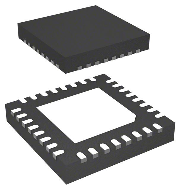
Small 32-pin QFN (5mm×5mm) Package
015000428-E-00
2015/01
-1-
�[AP1021]
3. Table of Contents
1.
2.
3.
4.
5.
6.
General Description ................................................................................................................................... 1
Features ...................................................................................................................................................... 1
Table of Contents ....................................................................................................................................... 2
Block Diagram ........................................................................................................................................... 3
Ordering Guide .......................................................................................................................................... 4
Pin Configurations and Functions .............................................................................................................. 4
■ Pin Configurations ................................................................................................................................... 4
■ Pin Functions ........................................................................................................................................... 5
7. Absolute Maximum Ratings ...................................................................................................................... 6
8. Recommended Operation Condition.......................................................................................................... 6
9. Electrical Characteristics ........................................................................................................................... 7
10.
Functional Descriptions ......................................................................................................................... 8
■ Enable mode ............................................................................................................................................ 8
■ ISn terminal current ................................................................................................................................. 9
■ SPI Interface .......................................................................................................................................... 14
■ Register map .......................................................................................................................................... 17
■ Register Description .............................................................................................................................. 17
11.
Recommended External Circuits.......................................................................................................... 20
12.
Package ................................................................................................................................................ 22
■ Outline Dimensions ............................................................................................................................... 22
■ Marking ................................................................................................................................................. 22
13.
Revise History ...................................................................................................................................... 23
IMPORTANT NOTICE .................................................................................................................................. 24
015000428-E-00
2015/01
-2-
�[AP1021]
4. Block Diagram
M
VM
M
CVM
OUT2A
OUT2B
OUT3A
OUT1B
OUT1A
OUT4B
OUT4A
OUT3B
VM
CVG
VG
Charge
Pump
VREF
VREF
RR1
1/2.5
VIS
CIVS
RR2
Iout=VIS / (2.5×RIS)
OSC
H-bridge
Current Control
UVLO
TSD
VREF
Control Logic
VC
LV
EN
SDO
CSN,SDI,SCK, IS1
5 OE12,OE34
IS2
IS3
IS4
RIS1
RIS2
RIS3
RIS4
Exposed
Pad
CLV
VC
CVC
CPU
Figure 1. Block Diagram
015000428-E-00
2015/01
-3-
�[AP1021]
5. Ordering Guide
AP1021 AEN
-40~85C
32-pin QFN
6. Pin Configurations and Functions
OUT3A
IS3
IS3
OUT3B
VM
OUT4A
IS4
IS4
24
23
22
21
20
19
18
17
■ Pin Configurations
SCK
25
16
OUT4B
SDI
26
15
VC
27
14
LV
13
VREF
12
VIS
11
TEST1
10
EN
9
OUT2B
SDO
28
OE12
29
OE34
30
TEST2
31
(Top View)
Exposed pad
2
3
2
4
5
6
7
8
IS1
IS1
OUT1B
VM
OUT2A
IS2
IS2
32
1
VG
AP1021
OUT1A
CSN
Exposed Pad must be connected to GND.
015000428-E-00
2015/01
-4-
�[AP1021]
■ Pin Functions
No.
Pin
Name
1
OUT1A A
O
Motor driver output
2, 3
IS1
IO
Current sense terminal
4
OUT1B A
O
Motor driver output
5, 20
VM
-
Motor driver power supply
6
OUT2A A
O
Motor driver output
7, 8
IS2
IO
Current sense terminal
9
OUT2B A
O
Motor driver output
10
EN
D
I
Chip Enable (Power save)
11
TEST1
A
I
TEST pin. This pin must be connected
to the ground.
12
VIS
A
I
Motor current set voltage input
13
VREF
A
O
Voltage reference
14
LV
A
O
Logic voltage output capacitor
connection
15
VC
P
-
Control power supply
16
OUT4B A
O
Motor driver output
17, 18
IS4
I
Current sense terminal
19
OUT4A A
O
Motor driver output
21
OUT3B A
O
Motor driver output
22, 23
IS3
IO
Current sense terminal
24
OUT3A A
O
Motor driver output
25
SCK
D
I
Control data clock
26
SDI
D
I
Control data input
27
CSN
D
I
Chip select
28
SDO
D
I
Control data output
29
OE12
D
I
30
OE34
D
I
31
TEST2
D
I
32
VG
A
IO
Charge-pump output voltage
EP
GND
-
Ground
Exposed
Pad
Note 1.
Note 2.
Note 3.
Type
(Note 1)
A
P
A
A
A
I/O
Function
(Note 2)
Remark
200k Pull-down
OUT1/2 Output Enable when SELOE
register bit=H
OUT3/4 Output Enable when SELOE
register bit=H
TEST pin. This pin must be connected
to the ground.
(Note 3)
A(analog pin), D(digital pin), GND(ground pin), P(power pin)
I(input pin), O(output pin), IO(input/output pin)
Exposed Pad must be connected to GND.
015000428-E-00
2015/01
-5-
�[AP1021]
7. Absolute Maximum Ratings
Parameter
Control supply voltage
Motor driver supply voltage
VC level terminal
(EN, CSN, SCK, SDI, SDO, OE12, OE34)
VM level terminal
(OUTnA, OUTnB)
1.8V level terminal
(LV, VREF, VIS)
1.2V level terminal
(ISn)
Symbol
VC
min
-0.5
max
5.5
Unit
V
VM
-0.5
32
V
Vterm1
-0.5
VC
V
Vterm2
-0.5
VM
V
Vterm3
-0.5
1.9
V
Vterm4
-0.5
1.3
V
Remark
IloadDC
1.2
A
Dual use (Note 8)
IloadPeak
1.7
A
Single use (Note 9)
Ipulse
2.8
A
Pulsed tw
很抱歉,暂时无法提供与“AP1021AEN”相匹配的价格&库存,您可以联系我们找货
免费人工找货