ADVANCED
LINEAR
DEVICES, INC.
ALD1105
DUAL N-CHANNEL AND DUAL P-CHANNEL MATCHED MOSFET PAIR
GENERAL DESCRIPTION
APPLICATIONS
The ALD1105 is a monolithic dual N-channel and dual P-channel complementary matched transistor pair intended for a broad range of analog
applications. These enhancement-mode transistors are manufactured
with Advanced Linear Devices' enhanced ACMOS silicon gate CMOS
process. It consists of an ALD1116 N-channel MOSFET pair and an
ALD1117 P-channel MOSFET pair in one package. The ALD1105 is a low
drain current, low leakage current version of the ALD1103.
•
•
•
•
•
•
•
•
•
•
The ALD1105 offers high input impedance and negative current temperature coefficient. The transistor pair is matched for minimum offset voltage
and differential thermal response, and it is designed for precision signal
switching and amplifying applications in +2V to +10V systems where low
input bias current, low input capacitance and fast switching speed are
desired. Since these are MOSFET devices, they feature very large
(almost infinite) current gain in a low frequency, or near DC, operating
environment. When used in pairs, a dual CMOS analog switch can be
constructed. In addition, the ALD1105 is intended as a building block for
differential amplifier input stages, transmission gates, and multiplexer
applications.
Precision current mirrors
Complementary push-pull linear drives
Analog switches
Choppers
Differential amplifier input stage
Voltage comparator
Data converters
Sample and Hold
Analog inverter
Precision matched current sources
PIN CONFIGURATION
The ALD1105 is suitable for use in precision applications which require
very high current gain, beta, such as current mirrors and current sources.
The high input impedance and the high DC current gain of the Field Effect
Transistors result in extremely low current loss through the control gate.
The DC current gain is limited by the gate input leakage current, which is
specified at 100pA at room temperature. For example, DC beta of the
device at a drain current of 3mA at 25°C is = 3mA/100pA = 300,000,000.
DN1
1
14
DN2
GN1
2
13
GN2
SN1
3
12
SN2
V-
4
11
V+
DP1
5
10
DP2
GP1
6
9
GP2
SP1
7
8
SP2
TOP VIEW
SBL, PBL PACKAGES
FEATURES
• Thermal tracking between N-channel and P-channel pairs
• Low threshold voltage of 0.7V for both N-channel &
P-channel MOSFETS
• Low input capacitance
• Low Vos -- 10mV
• High input impedance -- 1013Ω typical
• Low input and output leakage currents
• Negative current (IDS) temperature coefficient
• Enhancement mode (normally off)
• DC current gain 109
• Matched N-channel and matched P-channel in one package
• RoHS compliant
BLOCK DIAGRAM
N GATE 1 (2)
N SOURCE 1 (3)
N DRAIN 1 (1)
SUBSTRATE (4)
N SOURCE 2 (12)
N DRAIN 2 (14)
N GATE 2 (13)
ORDERING INFORMATION (“L” suffix denotes lead-free (RoHS))
P GATE 1 (6)
Operating Temperature Range*
0°C to +70°C
0°C to +70°C
P SOURCE 1 (7)
P DRAIN 1 (5)
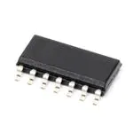
14-Pin
SOIC
Package
14-Pin
Plastic Dip
Package
ALD1105SBL
ALD1105PBL
SUBSTRATE (11)
P DRAIN 2 (10)
* Contact factory for high temperature versions.
©2021 Advanced Linear Devices, Inc., Vers. 2.2
P SOURCE 2 (8)
P GATE 2 (9)
www.aldinc.com
1 of 8
�ABSOLUTE MAXIMUM RATINGS
Drain-source voltage, VDS
Gate-source voltage, VGS
Power dissipation
Operating temperature range SBL, PBL packages
Storage temperature range
Lead temperature, 10 seconds
CAUTION: ESD Sensitive Device. Use static control procedures in ESD controlled environment.
10V
10V
500mW
0°C to +70°C
-65°C to +150°C
+260°C
OPERATING ELECTRICAL CHARACTERISTICS
TA = 25°C unless otherwise specified
Parameter
N - Channel
Symbol Min
Typ Max
Gate Threshold VT
Voltage
Offset Voltage
VGS1 - VGS2
0.4
VOS
Gate Threshold
Temperature
TCVT
Drift
Unit
Test
Conditions
0.7
1.0
V
IDS = 1µA VGS = VDS
2
10
mV
IDS = 10µA VGS = VDS
-1.2
P - Channel
Min
Typ Max
Unit
-0.4
V
IDS = -1µA VGS = VDS
mV
IDS = -10µA VGS = VDS
mV/°C
-0.7
-1.2
2
10
-1.3
On Drain
Current
IDS(ON)
3
4.8
mA
VGS = VDS = 5V
-1.3
-2
Trans-.
conductance
Gfs
1
1.8
mmho
VDS = 5V IDS = 10mA
0.25
0.67
Mismatch
∆Gfs
0.5
%
Output
Conductance
GOS
200
µmho
Drain Source
ON Resistance
RDS(ON)
350
Drain Source
ON Resistance ∆RDS(ON)
Mismatch
0.5
Drain Source
Breakdown
Voltage
BVDSS
Off Drain
Current
IDS(OFF)
Gate Leakage
Current
Input
Capacitance
ALD1105
500
10
Test
Conditions
mV/°C
mA
VGS = VDS = -5V
mmho
VDS = -5V IDS = -10mA
0.5
%
VDS = 5V IDS = 10mA
40
µmho
VDS = -5V IDS = -10mA
Ω
VDS = 0.1V VGS = 5V
1200
Ω
VDS = -0.1V VGS = -5V
%
VDS = 0.1V VGS = 5V
0.5
%
VDS = -0.1V VGS = -5V
V
IDS = 1µA VGS = 0V
V
IDS = -1µA VGS = 0V
1800
-10
10
400
4
pA
nA
VDS = 10V IGS = 0V
TA = 125°C
10
400
4
pA
nA
VDS = -10V VGS = 0V
TA = 125°C
IGSS
1
100
10
pA
nA
VDS = 0V VGS = 10V
TA = 125°C
1
100
10
pA
nA
VDS = 0V VGS = -10V
TA = 125°C
CISS
1
3
pF
1
3
pF
Advanced Linear Devices
2 of 8
�TYPICAL N-CHANNEL PERFORMANCE CHARACTERISTICS
OUTPUT CHARACTERISTICS
LOW VOLTAGE OUTPUT
CHARACTERISTICS
1000
VBS = 0V
TA = +25°C
DRAIN-SOURCE ON CURRENT
IDS(ON) (µA)
DRAIN SOURCE ON CURRENT
IDS(ON) (mA)
20
VGS = 10V
15
8V
10
6V
4V
5
2V
500
4V
2V
0
-500
-1000
0
0
2
6
4
8
10
TA = +25°C
2
1
0.5
IDS = 1mA
0.2
0
DRAIN SOURCE ON RESISTANCE
RDS(ON) (KΩ)
DRAIN SOURCE ON CURRENT
IDS(ON) (µA)
TA = +125°C
2
TRANSFER CHARACTERISTIC
WITH SUBSTRATE BIAS
4
6
VGS = VDS
TA = +25°C
VBS = 0V
-2V
15
-4V
-6V
10
-8V
5
-10V
0
8
0
10
1.6
0.8
2.4
3.2
DRAIN SOURCE ON VOLTAGE - VDS(ON) (V)
GATE SOURCE ON VOLTAGE - VGS(ON) (V)
DRAIN SOURCE ON RESISTANCE vs.
GATE-SOURCE VOLTAGE
DRAIN SOURCE OFF CURRENT vs.
AMBIENT TEMPERATURE
100
4.0
1000
DRAIN SOURCE OFF CURRENT
RDS(OFF) (pA)
FORWARD TRANSCONDUCTANCE
(mmho)
IDS = 10mA
5
+160
20
VBS = 0V
f = 1KHz
10
+80
DRAIN SOURCE ON VOLTAGE - VDS(ON) (mV)
FORWARD TRANSCONDUCTANCE vs.
DRAIN-SOURCE VOLTAGE
20
0
-80
-160
DRAIN SOURCE ON VOLTAGE - VDS(ON) (V)
VDS = 0.2V
VBS = 0V
10
TA = +125°C
1
TA = +25°C
0.1
0
2
4
6
8
VDS = 10V
VGS = VBS = 0V
100
10
1
10
GATE SOURCE ON VOLTAGE - VGS(ON) (V)
ALD1105
VGS = 10V
8V
6V
VBS = 0V
TA = 25°C
Advanced Linear Devices
-50
-25
0
+25
+50
+75
+100 +125
AMBIENT TEMPERATURE - TA (°C)
3 of 8
�TYPICAL P-CHANNEL PERFORMANCE CHARACTERISTICS
OUTPUT CHARACTERISTICS
LOW VOLTAGE OUTPUT
CHARACTERISTICS
500
DRAIN SOURCE ON CURRENT
IDS(ON) (µA)
DRAIN SOURCE ON CURRENT
IDS(ON) (mA)
-10
VBS = 0V
TA = +25°C
-7.5
VGS = -10V
-5.0
-8V
-6V
-2.5
-4V
-2V
250
-4V
-2V
0
-250
-500
0
0
-4
-2
-6
-8
-10
+320
TRANSFER CHARACTERISTIC
WITH SUBSTRATE BIAS
1.0
-20
DRAIN SOURCE ON CURRENT
IDS(ON) (µA)
IDS = -5mA
TA = +25°C
0.5
0.2
0.1
TA = +125°C
0.05
IDS = -1mA
VBS = 0V
f = 1KHz
0.02
0.01
VBS = 0V
2V
4V
6V
8V
10V
-15
-10
-5
VGS = VDS
TA = +25°C
0
0
-2
-4
-6
-8
-10
0
-1.6
-0.8
-2.4
-3.2
-4.0
DRAIN SOURCE ON VOLTAGE - VDS(ON) (V)
GATE SOURCE ON VOLTAGE - VGS(ON) (V)
DRAIN SOURCE ON RESISTANCE vs.
GATE-SOURCE VOLTAGE
DRAIN SOURCE OFF CURRENT vs.
AMBIENT TEMPERATURE
1000
100
DRAIN SOURCE OFF CURRENT
RDS(OFF) (pA)
FORWARD TRANSCONDUCTANCE
(mmho)
+160
DRAIN SOURCE ON VOLTAGE - VDS(ON) (mV)
FORWARD TRANSCONDUCTANCE vs.
DRAIN-SOURCE VOLTAGE
DRAIN SOURCE ON RESISTANCE
RDS(ON) (KΩ)
0
-160
-320
DRAIN SOURCE ON VOLTAGE - VDS(ON) (V)
VDS = 0.4V
VBS = 0V
TA = +125°C
10
1
TA = +25°C
0.1
0
-2
-4
-6
-8
VDS = -10V
VGS = VBS = 0V
100
10
1
-10
GATE SOURCE ON VOLTAGE - VGS(ON) (V)
ALD1105
VGS = -10V
-8V
-6V
VBS = 0V
TA = 25°C
Advanced Linear Devices
-50
-25
0
+25
+50
+75
+100 +125
AMBIENT TEMPERATURE - TA (°C)
4 of 8
�TYPICAL APPLICATIONS
CURRENT SOURCE MIRROR
CURRENT SOURCE WITH GATE CONTROL
V+ = +5V
V+ = +5V
1/2 ALD1105
V+ = +5V
Q3
ISET
Q4
Q3
Q4
RSET
ISET
ISOURCE
Q1
Digital Logic Control
of Current Source
ISOURCE = ISET
V+ - Vt
=
RSET
4
~
= R
SET
Q2
ALD1105
ISOURCE
RSET
ON
Q1
1/4 ALD1105
OFF
Q1 : N-Channel MOSFET
Q3, Q4: P-Channel MOSFET
Q1, Q2: N-Channel MOSFET
Q3, Q4: P-Channel MOSFET
DIFFERENTIAL AMPLIFIER
CURRENT SOURCE MULTIPLICATION
V+
V+ = +5V
ISOURCE = ISET x N
PMOS PAIR
Q3
ISET
RSET
ISOURCE
Q4
VOUT
VIN+
Q1
ALD1105
Q2
NMOS PAIR
QSET
Q2
Q3
QN
Current
Source
QSET, Q1..QN: ALD1106 or ALD1105
N-Channel MOSFET
Q1, Q2: N-Channel MOSFET
Q3, Q4: P-Channel MOSFET
ALD1105
Q1
VIN-
Advanced Linear Devices
5 of 8
�TYPICAL APPLICATIONS (cont.)
BASIC CURRENT SOURCES
N-CHANNEL CURRENT SOURCE
P-CHANNEL CURRENT SOURCE
V+ = +5V
V+ = +5V
RSET
ISET
1/2 ALD1105
ISOURCE
Q2
Q3
Q1
ISOURCE = ISET
V+ - Vt
=
RSET
V+ - 1.0
~
= R
SET
4
~
= R
SET
1/2 ALD1105
Q4
ISOURCE
ISET
RSET
Q3, Q4: P-Channel MOSFET
Q1, Q2: N-Channel MOSFET
CASCODE CURRENT SOURCES
V+ = +5V
V+ = +5V
ISET
RSET
ISOURCE
Q4
Q2
Q1
Q2
Q3
Q4
Q3
Q1
ISET
RSET
ISOURCE = ISET =
Q1, Q2, Q3, Q4: N-Channel MOSFET
(1/2 ALD1105 or ALD1116)
ALD1105
ISOURCE
3
V+ - 2Vt ~
RSET = RSET
Q1, Q2, Q3, Q4: P-Channel MOSFET
(1/2 ALD1105 or ALD1117)
Advanced Linear Devices
6 of 8
�SOIC-14 PACKAGE DRAWING
14 Pin Plastic SOIC Package
Millimeters
E
S (45°)
Dim
Min
A
1.35
Max
1.75
Min
0.053
Max
0.069
A1
0.10
0.25
0.004
0.010
b
0.35
0.45
0.014
0.018
C
0.18
0.25
0.007
0.010
D-14
8.55
8.75
0.336
0.345
E
3.50
4.05
0.140
0.160
1.27 BSC
e
D
A
Inches
0.050 BSC
H
5.70
6.30
0.224
0.248
L
0.60
0.937
0.024
0.037
ø
0°
8°
0°
8°
S
0.25
0.50
0.010
0.020
A1
e
b
S (45°)
H
L
ALD1105
C
ø
Advanced Linear Devices
7 of 8
�PDIP-14 PACKAGE DRAWING
14 Pin Plastic DIP Package
Millimeters
E
E1
D
S
A2
A1
e
b
b1
A
L
Dim
A
A1
Min
Inches
3.81
Max
5.08
Min
0.105
Max
0.200
0.38
1.27
0.015
0.050
A2
1.27
2.03
0.050
0.080
b
0.89
1.65
0.035
0.065
b1
0.38
0.51
0.015
0.020
c
0.20
0.30
0.008
0.012
D-14
17.27
19.30
0.680
0.760
E
5.59
7.11
0.220
0.280
E1
7.62
8.26
0.300
0.325
e
2.29
2.79
0.090
0.110
e1
7.37
7.87
0.290
0.310
L
2.79
3.81
0.110
0.150
S-14
1.02
2.03
0.040
0.080
ø
0°
15°
0°
15°
c
e1
ALD1105
ø
Advanced Linear Devices
8 of 8
�
很抱歉,暂时无法提供与“ALD1105SBL”相匹配的价格&库存,您可以联系我们找货
免费人工找货