A1140/41/42/43
Sensitive Two-Wire Chopper-Stabilized Unipolar Hall-Effect Switches
The A1140, A1141, A1142, and A1143 devices are sensitive, two-wire, unipolar, Hall effect switches that are factory-programmed at end-of-line to optimize magnetic switchpoint accuracy. These devices are produced on the Allegro MicroSystems advanced BiCMOS wafer fabrication process, which implements a patented, high-frequency, chopper-stabilization technique that achieves magnetic stability and eliminates the offsets that are inherent in single-element devices exposed to harsh application environments. Commonly found in a number of automotive applications, the A1140-43 family of devices are utilized to sense: seat track position, seat belt buckle presence, hood/trunk latching, and shift selector position. Two-wire unipolar switches are particularly advantageous in price-sensitive applications, because they require one less wire than the more traditional open-collector output switches. Additionally, the system designer gains inherent diagnostics because output current normally flows in either of two narrowly-specified ranges. Any output current level outside of these two ranges is a fault condition. The A1140-43 family of devices also features on-chip transient protection, and a Zener clamp to protect against overvoltage conditions on the supply line. The output currents of the A1141 and A1143 switch HIGH in the presence of a south polarity magnetic field of sufficient strength; and switch LOW otherwise, including when there is no significant magnetic field present. The A1140 and A1142 have inverted output current levels: switching LOW in the presence of a south polarity magnetic field of sufficient strength, and HIGH otherwise. The devices also differ in their specified LOW current supply levels. All family members are offered in two package styles: SOT-23W, a miniature lowprofile package for surface-mount applications (suffix –LH), and TO-92, threelead ultra-mini Single Inline Package (SIP) for through-hole mounting (suffix –UA). Field-programmable versions are also available. Refer to: A1180, A1181, A1182, and A1183.
Package LH, 3-pin SOT
3
1. VCC 2. No connection 3. GND
NC 1 2
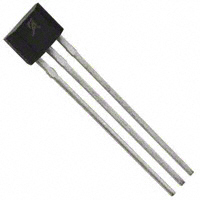
Package UA, 3-pin SIP
1. VCC 2. GND 3. GND
1 2
PTCT
3
ABSOLUTE MAXIMUM RATINGS
Supply Voltage, VCC .......................................... 28 V Reverse-Supply Voltage, VRCC ........................ –18 V Magnetic Flux Density, B .........................Unlimited Operating Temperature Ambient, TA, Range E.................. –40ºC to 85ºC Ambient, TA, Range L................ –40ºC to 150ºC Maximum Junction, TJ(max)........................165ºC Storage Temperature, TS .................. –65ºC to 170ºC
Features and Benefits
Chopper stabilization Low switchpoint drift over operating temperature range Low stress sensitivity Factory programmed at end-of-line for optimized switchpoints On-chip protection Supply transient protection Reverse-battery protection On-board voltage regulator 3.5 V to 24 V operation
A1140-DS
Allegro MicroSystems, Inc. 115 Northeast Cutoff, Box 15036 Worcester, Massachusetts 01615-0036 (508) 853-5000 www.allegromicro.com
�A1140/41/42/43
Sensitive Two-Wire Chopper-Stabilized Unipolar Hall Effect Switches Functional Block Diagram
V+ VCC Program/Lock Programming Logic Offset
Regulator Clock/Logic 0.01 uF Sample and Hold Dynamic Offset Cancellation Low-Pass Filter
Amp
GND Package UA Only
GND
Product Selection Guide
Use the complete part numbers when ordering
Supply Current at Low Output, ICC(L) (mA) Output South (+) Field1 Other Field2
Part Number A1140ELH A1140EUA A1140LLH A1140LUA A1141ELH A1141EUA A1141LLH A1141LUA A1142ELH A1142EUA A1142LLH A1142LUA A1143ELH A1143EUA A1143LLH A1143LUA
1South 2Includes
Package Surface Mount SIP Surface Mount SIP Surface Mount SIP Surface Mount SIP Surface Mount SIP Surface Mount SIP Surface Mount SIP Surface Mount SIP
TA (ºC) –40 to 85
2 to 5 –40 to 150 –40 to 85 2 to 5 –40 to 150 –40 to 85 5 to 6.9 –40 to 150 –40 to 85 5 to 6.9 –40 to 150
Low
High
High
Low
Low
High
High
Low
(+) magnetic fields must be of sufficient strength. north (–) magnetic fields of sufficient strength, and weak fields of either polarity.
A1140-DS
Allegro MicroSystems, Inc. 115 Northeast Cutoff, Box 15036 Worcester, Massachusetts 01615-0036 (508) 853-5000 www.allegromicro.com
2
�A1140/41/42/43
Sensitive Two-Wire Chopper-Stabilized Unipolar Hall Effect Switches
ELECTRICAL CHARACTERISTICS over the operating voltage and temperature range, unless otherwise specified
Characteristic Supply Voltage Symbol VCC ICC(L) ICC(H) Zener Clamp Supply Voltage Zener Clamp Supply Current2 Output Slew Rate3 Chopping Frequency Power-On Time4 Power-On State5
1Relative
Test Conditions Device powered on B >BOP for A1140; B BOP for A1142; B BOP for A1141, A1143 B t CC on on(max), and BRP < B < BOP, POS is undefined.
MAGNETIC CHARACTERISTICS* over the operating voltage and temperature range, unless otherwise specified
Characteristic Operate Point Release Point Hysteresis Symbol BOP BRP BHYS Test Conditions ICC(H) → ICC(L) ICC(L) → ICC(H) ICC(L) → ICC(H) ICC(H) → ICC(L) for A1140, A1142 for A1141, A1143 for A1140, A1142 for A1141, A1143 Min. 50 45 5 Typ. 85 – 15 Max. 115 110 30 Units G G G
BHYS = BOP – BRP
*Relative values of B use the algebraic convention, where positive values indicate south magnetic polarity, and negative values indicate north magnetic polarity; therefore greater B values indicate a stronger south polarity field (or a weaker north polarity field, if present).
A1140-DS
Allegro MicroSystems, Inc. 115 Northeast Cutoff, Box 15036 Worcester, Massachusetts 01615-0036 (508) 853-5000 www.allegromicro.com
3
�A1140/41/42/43
Sensitive Two-Wire Chopper-Stabilized Unipolar Hall Effect Switches Characteristic Data
ICC(L) versus Ambient Temperature at Various Levels of VCC (A1140, A1141, A1142, A1143)
20 18
10 8
ICC(H) versus Ambient Temperature at Various Levels of VCC (A1140, A1141, A1142, A1143)
ICC(L) (mA)
6 4 2 0
ICC(H) (mA)
VCC 3.8 V 12.0 V 24.0 V
VCC
16 14 12 10
3.8 V 12.0 V 24.0 V
–40
25
150
–40
Ambient Temperature, TA (°C)
25 150 Ambient Temperature, TA (°C)
110 105 100 95 85 80 75 70 65 60 55 –50 90 BOP (G)
Switchpoint versus Ambient Temperature (A1143)
30 25 BHYS (G) 20 15 10
Hysteresis versus Ambient Temperature (A1143)
0
50
100
150
200
5 –50
0
50
100
150
200
Ambient Temperature, TA (°C)
Ambient Temperature, TA (°C)
Contact Allegro MicroSystems for information.
Device Qualification Program
EMC (Electromagnetic Compatibility) Requirements
Contact your local representative for EMC results.
Test Name ESD – Human Body Model ESD – Machine Model Conducted Transients Direct RF Injection Bulk Current Injection TEM Cell Reference Specification AEC-Q100-002 AEC-Q100-003 ISO 7637-1 ISO 11452-7 ISO 11452-4 ISO 11452-3
Allegro MicroSystems, Inc. 115 Northeast Cutoff, Box 15036 Worcester, Massachusetts 01615-0036 (508) 853-5000 www.allegromicro.com
4
A1140-DS
�A1140/41/42/43
Sensitive Two-Wire Chopper-Stabilized Unipolar Hall Effect Switches
THERMAL CHARACTERISTICS may require derating at maximum conditions, see application information
Characteristic Symbol Test Conditions Package LH, minimum-K PCB (single-sided with copper limited to solder pads) Package LH, low-K PCB (double-sided with 0.926 in2 copper area) Package UA, minimum-K PCB (single-sided with copper limited to solder pads) Min. 110 228 165 Typ. – – – Max Units – – – ºC/W ºC/W ºC/W
Package Thermal Resistance
RθJA
25 24 23 22 21 20 19 18 17 16 15 14 13 12 11 10 9 8 7 6 5 4 3 2 20
Power Derating Curve TJ(max) = 165ºC; ICC = ICC(max)
VCC(max)
Maximum Allowable VCC (V)
Low-K PCB, Package LH (RθJA = 110 ºC/W) Minimum-K PCB, Package UA (RθJA = 165 ºC/W) Minimum-K PCB, Package LH (RθJA = 228 ºC/W) VCC(min)
140 160 180
40
60
80
100
120
1900 1800 1700 1600 1500 1400 1300 1200 1100 1000 900 800 700 600 500 400 300 200 100 0 20
Maximum Power Dissipation, PD(max) TJ(max) = 165ºC; VCC = VCC(max); ICC = ICC(max)
Power Dissipation, PD (m W)
Lo (R w-K PC θJ A= 11 B, P 0 º ac Min C/ ka W ge (R imum ) LH -K θJA = PC 165 B, P ºC/ ack W) age UA Min imu m-K (R P θJA = 228 CB, Pa ºC/W ckag e LH )
40
60
80 100 120 Temperature (°C)
140
160
180
A1140-DS
Allegro MicroSystems, Inc. 115 Northeast Cutoff, Box 15036 Worcester, Massachusetts 01615-0036 (508) 853-5000 www.allegromicro.com
5
�A1140/41/42/43
Sensitive Two-Wire Chopper-Stabilized Unipolar Hall Effect Switches
Functional Description
Operation The output, ICC, of the A1140 and A1142 devices switch low after the magnetic field at the Hall sensor exceeds the operate point threshold, BOP. When the magnetic field is reduced to below the release point threshold, BRP, the device output goes high. The differences between the magnetic operate and release point is called the hysteresis of the device, BHYS. This builtin hysteresis allows clean switching of the output even in the presence of external mechanical vibration and electrical noise. The A1141 and A1143 devices switch with opposite polarity for similar BOP and BRP values, in comparison to the A1140 and A1142 (see figure 1).
I+ ICC(H)
I+ ICC(H)
Switch to High
ICC(L) 0
Switch to High
Switch to Low
Switch to Low
ICC
ICC
ICC(L) 0
BRP
BHYS
BHYS
(A) A1140, A1142
(B) A1141, A1143
Figure 1. Alternative switching behaviors are available in the A114x device family. On the horizontal axis, the B+ direction indicates increasing south polarity magnetic field strength, and the B– direction indicates decreasing south polarity field strength (including the case of increasing north polarity).
BOP
B–
B+
B–
B+
BRP
BOP
A1140-DS
Allegro MicroSystems, Inc. 115 Northeast Cutoff, Box 15036 Worcester, Massachusetts 01615-0036 (508) 853-5000 www.allegromicro.com
6
�A1140/41/42/43
Sensitive Two-Wire Chopper-Stabilized Unipolar Hall Effect Switches
Chopper Stabilization Technique When using Hall-effect technology, a limiting factor for switchpoint accuracy is the small signal voltage developed across the Hall element. This voltage is disproportionally small relative to the offset that can be produced at the output of the Hall sensor. This makes it difficult to process the signal while maintaining an accurate, reliable output over the specified operating temperature and voltage ranges. Chopper stabilization is a unique approach used to minimize Hall offset on the chip. The patented Allegro technique, namely dynamic quadrature offset cancellation, removes key sources of the output drift induced by thermal and mechanical stresses. This offset reduction technique is based on a signal modulationdemodulation process. The undesired offset signal is separated from the magnetic field-induced signal in the frequency domain, through modulation. The subsequent demodulation acts as a modulation process for the offset, causing the magnetic fieldinduced signal to recover its original spectrum at baseband, while the dc offset becomes a high-frequency signal. The magneticsourced signal then can pass through a low-pass filter, while the modulated dc offset is suppressed. The chopper stabilization technique uses a 200 kHz high frequency clock. The chopping occurs on each clock edge, resulting in a 400 kHz chop frequency. This high-frequency operation allows a greater sampling rate, which results in higher accuracy and faster signal-processing capability. This approach desensitizes the chip to the effects of thermal and mechanical stresses, and produces devices that have extremely stable quiescent Hall output voltages and precise recoverability after temperature cycling. This technique is made possible through the use of a BiCMOS process, which allows the use of low-offset, low-noise amplifiers in combination with high-density logic integration and sample-and-hold circuits. This process is illustrated in figure 2. The repeatability of magnetic field-induced switching is affected slightly by a chopper technique. However, the Allegro high-frequency chopping approach minimizes the affect of jitter and makes it imperceptible in most applications. Applications that are more likely to be sensitive to such degradation are those requiring precise sensing of alternating magnetic fields; for example, speed sensing of ring-magnet targets. For such applications, Allegro recommends its digital sensor families with lower sensitivity to jitter. For more information on those devices, contact your Allegro sales representative.
Regulator
Clock/Logic Hall Element Amp Low-Pass Filter
Figure 2. Chopper stabilization circuit (dynamic quadrature offset cancellation)
Sample and Hold
A1140-DS
Allegro MicroSystems, Inc. 115 Northeast Cutoff, Box 15036 Worcester, Massachusetts 01615-0036 (508) 853-5000 www.allegromicro.com
7
�A1140/41/42/43
Sensitive Two-Wire Chopper-Stabilized Unipolar Hall Effect Switches Application Information
For additional general application information, visit the Allegro MicroSystems Web site at www. allegromicro.com.
Typical Application Circuit The A114x family of devices must be protected by an external bypass capacitor, CBYP, connected between the supply, VCC, and the ground, GND, of the device. CBYP reduces both external noise and the noise generated by the chopper-stabilization function. As shown in figure 3, a 0.01 µF capacitor is typical. Installation of CBYP must ensure that the traces that connect it to the A114x pins are no greater than 5 mm in length. All high-frequency interferences conducted along the supply lines are passed directly to the load through CBYP, and it serves only to protect the A114x internal circuitry. As a result, the load ECU (electronic control unit) must have sufficient protection, other than CBYP, installed in parallel with the A114x. A series resistor on the supply side, RS (not shown), in combination with CBYP, creates a filter for EMI pulses. (Additional information on EMC is provided on the Allegro MicroSystems Web site.) When determining the minimum VCC requirement of the A114x device, the voltage drops across RS and the ECU sense resistor, RSENSE, must be taken into consideration. The typical value for RSENSE is approximately 100 Ω.
GND A A B Package UA Only Maximum separation 5 mm V+
VCC
B
A114x
CBYP 0.01 uF
GND
B
RSENSE
ECU
Figure 3. Typical application circuit
A1140-DS
Allegro MicroSystems, Inc. 115 Northeast Cutoff, Box 15036 Worcester, Massachusetts 01615-0036 (508) 853-5000 www.allegromicro.com
8
�A1140/41/42/43
Sensitive Two-Wire Chopper-Stabilized Unipolar Hall Effect Switches
Power Derating The device must be operated below the maximum junction temperature of the device, TJ(max). Under certain combinations of peak conditions, reliable operation may require derating supplied power or improving the heat dissipation properties of the application. This section presents a procedure for correlating factors affecting operating TJ. (Thermal data is also available on the Allegro MicroSystems Web site.) The Package Thermal Resistance, RθJA, is a figure of merit summarizing the ability of the application and the device to dissipate heat from the junction (die), through all paths to the ambient air. Its primary component is the Effective Thermal Conductivity, K, of the printed circuit board, including adjacent devices and traces. Radiation from the die through the device case, RθJC, is relatively small component of RθJA. Ambient air temperature, TA, and air motion are significant external factors, damped by overmolding. The effect of varying power levels (Power Dissipation, PD), can be estimated. The following formulas represent the fundamental relationships used to estimate TJ, at PD. PD = VIN × IIN ∆T = PD × RθJA TJ = TA + ∆T (1) (2) (3) Example: Reliability for VCC at TA = 150°C, package UA, using minimum-K PCB. Observe the worst-case ratings for the device, specifically: RθJA = 165°C/W, TJ(max) = 165°C, VCC(max) = 24 V, and ICC(max) = 17 mA. Calculate the maximum allowable power level, PD(max). First, invert equation 3: ∆Tmax = TJ(max) – TA = 165 °C – 150 °C = 15 °C This provides the allowable increase to TJ resulting from internal power dissipation. Then, invert equation 2: PD(max) = ∆Tmax ÷ RθJA = 15°C ÷ 165 °C/W = 91 mW Finally, invert equation 1 with respect to voltage: VCC(est) = PD(max) ÷ ICC(max) = 91 mW ÷ 17 mA = 5 V The result indicates that, at TA, the application and device can dissipate adequate amounts of heat at voltages ≤VCC(est). Compare VCC(est) to VCC(max). If VCC(est) ≤ VCC(max), then reliable operation between VCC(est) and VCC(max) requires enhanced RθJA. If VCC(est) ≥ VCC(max), then operation between VCC(est) and VCC(max) is reliable under these conditions.
For example, given common conditions such as: TA= 25°C, VCC = 12 V, ICC = 4 mA, and RθJA = 140 °C/W, then: PD = VCC × ICC = 12 V × 4 mA = 48 mW ∆T = PD × RθJA = 48 mW × 140 °C/W = 7°C TJ = TA + ∆T = 25°C + 7°C = 32°C A worst-case estimate, PD(max), represents the maximum allowable power level (VCC(max), ICC(max)), without exceeding TJ(max), at a selected RθJA and TA.
A1140-DS
Allegro MicroSystems, Inc. 115 Northeast Cutoff, Box 15036 Worcester, Massachusetts 01615-0036 (508) 853-5000 www.allegromicro.com
9
�A1140/41/42/43
Sensitive Two-Wire Chopper-Stabilized Unipolar Hall Effect Switches Package LH, 3-Pin; (SOT-23W)
3.10 .122 2.90 .114 1.49 .059 NOM 3 0.28 .011 NOM 8º 0º 0.20 .008 0.13 .005
0.70 .028 BSC
C
0.96 .038 NOM 2.10 .083 1.85 .073 3.00 .118 2.70 .106 2.40 .094 BSC 0.25 .010 MIN 1.00 .039 BSC 1 2 0.25 .010 BSC Seating Plane Gauge Plane
A
A
0.95 .037 BSC Dimensions in millimeters U.S. Customary dimensions (in.) in brackets, for reference only Hall element Active Area Depth 0.28 [.011] Fits SC–59A Solder Pad Layout
0.50 .020 0.30 .012 0.55 .022 REF
1.13 .045 0.87 .034 0.95 .037 BSC 0.15 .006 0.00 .000
B C
Package UA, 3-Pin; (TO-92)
.164 4.17 .159 4.04 45° BSC .0195 0.50 NOM .0805 2.04 NOM .0565 1.44 NOM
B
.062 1.57 .058 1.47
.122 3.10 .117 2.97
45° BSC
.085 2.16 MAX
.031 0.79 REF A
.640 16.26 .600 15.24
1
2
3
.017 0.44 .014 0.35
.019 0.48 .014 0.36 .050 1.27 BSC Dimensions in inches Metric dimensions (mm) in brackets, for reference only A Dambar removal protrusion
B Hall element
A1140-DS
Allegro MicroSystems, Inc. 115 Northeast Cutoff, Box 15036 Worcester, Massachusetts 01615-0036 (508) 853-5000 www.allegromicro.com
10
�A1140/41/42/43
Sensitive Two-Wire Chopper-Stabilized Unipolar Hall Effect Switches
The products described herein are manufactured under one or more of the following U.S. patents: 5,045,920; 5,264,783; 5,442,283; 5,389,889; 5,581,179; 5,517,112; 5,619,137; 5,621,319; 5,650,719; 5,686,894; 5,694,038; 5,729,130; 5,917,320; and other patents pending. Allegro MicroSystems, Inc. reserves the right to make, from time to time, such departures from the detail specifications as may be required to permit improvements in the performance, reliability, or manufacturability of its products. Before placing an order, the user is cautioned to verify that the information being relied upon is current. Allegro products are not authorized for use as critical components in life-support devices or systems without express written approval. The information included herein is believed to be accurate and reliable. However, Allegro MicroSystems, Inc. assumes no responsibility for its use; nor for any infringement of patents or other rights of third parties which may result from its use. Copyright © 2004 Allegro MicroSystems, Inc.
A1140-DS
Allegro MicroSystems, Inc. 115 Northeast Cutoff, Box 15036 Worcester, Massachusetts 01615-0036 (508) 853-5000 www.allegromicro.com
11
�