A1171 Micropower Ultrasensitive Hall Effect Switch
Features and Benefits
▪ ▪ ▪ ▪ ▪ ▪ ▪ 1.65 to 3.5 V battery operation Low supply current High sensitivity, BOP typically 30 G (3.0 mT) Operation with either north or south pole Configurable unipolar or omnipolar magnetic sensing Complementary, push-pull outputs Chopper stabilized ▫ Superior temperature stability ▫ Extremely low switchpoint drift ▫ Insensitive to physical stress ▪ Solid state reliability ▪ Small size
Description
The A1171 integrated circuit is an ultrasensitive, Hall effect switch with latched digital outputs and either unipolar or omnipolar magnetic actuation. It features operation at low supply currents and voltages, making it ideal for batteryoperated electronics. The low operating supply voltage, 1.65 to 3.5 V, and unique clocking algorithm assist in reducing the average operating power consumption. For example, the power requirement is less than 15 μW with a 2.75 V supply. Unlike more traditional Hall effect switches, the A1171 allows the user to configure how the device is magnetically actuated. Under default conditions the device activates output switching with either a north or south polarity magnetic field of sufficient strength. The magnetic actuation can be set via an external selection pin to operate in a unipolar mode, switching only on a north or south polarity but not both. Furthermore, the output of the A1171 can be configured to switch either off or on in the absence of any significant magnetic field. Lastly, the A1171 has two push-pull output structures. This polarity-independence, as well as the minimal power requirements, allows the A1171 to easily replace reed switches,
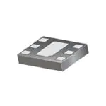
Package: 6 pin DFN/MLP (suffix EW)
Not to scale
Continued on the next page…
Functional Block Diagram
VDD
Clock / Logic Sample and Hold and Averaging Dynamic Offset Cancellation Low-Pass Filter Latch Logic
VOUTPS
Amp
Latch
VOUTPN
GND
1171-DS
SELECT
�A1171
Description (continued)
Micropower Ultrasensitive Hall Effect Switch
silicon chip, a Hall-voltage generator, a small-signal amplifier, chopper stabilization, a latch, and a MOSFET output. The A1171 device offers a magnetically optimized solution, suitable for most applications. Package type EW (0.40 mm maximum height) offers a leadless surface mount solution. It is lead (Pb) free, with NiPdAu leadframe plating.
providing superior reliability and ease of manufacturing while eliminating the requirement for signal conditioning. Improved stability is made possible through dynamic offset cancellation using chopper stabilization, which reduces the residual offset voltage normally caused by device overmolding, temperature dependencies, and thermal stress. This device includes, on a single
Selection Guide
Part Number
A1171EEWLT-P DFN/MLP 1.5� mm; 0.40 mm maximum height *Contact Allegro for additional packing options.
Package
3000 pieces per 7 inch reel
Packing*
Absolute Maximum Ratings
Characteristic Supply Voltage Reverse Supply Voltage Magnetic Flux Density Output Off Voltage Reverse Output Voltage Output Current Operating Ambient Temperature Maximum Junction Temperature Storage Temperature Symbol VDD VRDD B VOUTPx VROUTPx IOUTPx(Source) IOUTPx(Sink) TA TJ(max) Tstg Range E Notes Rating 5 –0.3 Unlimited 5 –0.3 1 –1 –40 to 85 165 –65 to 170 Units V V G V V mA mA ºC ºC ºC
Terminal List Table Pin-out Diagram
VOUTPS 1 VOUTPN 2 SELECT 3 PAD 6 VDD 5 NC 4 GND
Name VOUTPS VOUTPN SELECT GND NC VDD PAD Number 1 � 3 4 5 6 – Function Push-pull output (selectable omnipolar activation or unipolar south pole activation) Push-pull output (selectable inverted omnipolar activation or unipolar north pole activation) Sets activation mode for VOUTPx outputs; omnipolar output when tied to VDD or floating, unipolar output when grounded Ground No connection Connects power supply to chip Exposed pad for enhanced thermal dissipation
Allegro MicroSystems, Inc. 115 Northeast Cutoff Worcester, Massachusetts 01615-0036 U.S.A. 1.508.853.5000; www.allegromicro.com
�
�A1171
Micropower Ultrasensitive Hall Effect Switch
ELECTRICAL CHARACTERISTICS valid over operating voltage and temperature range (unless otherwise specified)
Characteristic Electrical Characteristics
Supply Voltage Range� Output Voltage Mode Cycle Period Chopping Frequency VDD VOUT(HIGH) tPeriod fC VOUT(SAT) Operating, TA= �5°C 1.65 1.8 – – – Device in awake mode (enabled) Device in sleep mode (disabled) VDD = 1.8 V, TA = �5°C VDD = 3.5 V, TA = �5°C – – – – 0 0
�/ V 3 DD
Symbol
Test Conditions
Min.
Typ.1
– 100 50 – – 3.5 7.1 1 – –
Max.
3.5 300 – 100 – �.0 8.0 8 1� �
1/ V 3 DD
Units
V mV mV ms kHz mA µA µA µA µA V V
Operating, over full ambient temperature range NMOS on, ISINK = 1 mA, VDD = 3.5 V PMOS on, ISOURCE = –1 mA, VDD = 3.5 V
VDD–300 VDD–100 �00
Supply Current SELECT Current3 SELECT Voltage3
1Typical
IDD(DIS) IDD(AV) VSELECT(LOW) ISELECT
IDD(EN)
VSELECT(HIGH)
VDD
data are for initial design estimations only, and assume optimum manufacturing and application conditions, such as TA = �5°C. Performance may vary for individual units, within the specified maximum and minimum limits. �Operate points, B OPX, and release points, BRPX, vary with supply voltage. 3Maximum V , minimum 0 V. DD
MAGNETIC CHARACTERISTICS valid at 1.8 V ≤ VDD ≤ 3.5 V and TA = �5°C
Characteristic Symbol
BOPN BRPN BHYS BRPS BOPS
Test Conditions
Min.
– –55 6 –
Typ.1
3� –3� �6 –�6 6
Max.
55 – – –6 –
Units2
G G G G G
Operate Point3 Release Point3 Hysteresis
1Typical
|BOPX - BRPX|
–
data are for initial design estimations only, and assume optimum manufacturing and application conditions, such as TA = �5°C. Performance may vary for individual units, within the specified maximum and minimum limits. �1 gauss (G) is exactly equal to 0.1 millitesla (mT). 3Operate points, B OPX, and release points, BRPX, vary with supply voltage.
Allegro MicroSystems, Inc. 115 Northeast Cutoff Worcester, Massachusetts 01615-0036 U.S.A. 1.508.853.5000; www.allegromicro.com
3
�A1171
Micropower Ultrasensitive Hall Effect Switch
THERMAL CHARACTERISTICS may require derating at maximum conditions, see application information
Characteristic Package Thermal Resistance Symbol RθJA �-layer PCB, with 0.�3 Test Conditions* in.� copper area each side 4-layer PCB, based on JEDEC standard Value 1�5 64 Units ºC/W ºC/W
*Additional thermal information available on Allegro Web site.
Power Dissipation versus Ambient Temperature Power Dissipation versus Ambient Temperature
3000 2750 2500 2250
Power Dissipation, PD (mW)
2000 1750 1500 1250 1000 750 500 250 0 20 40 60
EW package 2-layer PCB (RθJA = 125 ºC/W)
EW package 4-layer PCB (RθJA = 64 ºC/W)
80 100 120 Temperature (°C)
140
160
180
Output Polarity Diagram
+B (South)
Magnetic Field
0
–B (North)
(Omnipolar configuration)
VOUTPS VOUTPN
Output Pin (Activation Polarity)
(Unipolar configuration)
(South) VOUTPS (North) VOUTPN
Allegro MicroSystems, Inc. 115 Northeast Cutoff Worcester, Massachusetts 01615-0036 U.S.A. 1.508.853.5000; www.allegromicro.com
4
�A1171
Micropower Ultrasensitive Hall Effect Switch
Functional Description
Low Average Power Internal timing circuitry activates the sensor for a short period of time, tAwake, and deactivates it for the remainder of the period (tPeriod). A short awake state duration allows stabilization prior to the sensor sampling and data-latching on the falling edge of the timing pulse. The output during the sleep state is latched in the last sampled state. The supply current is not affected by the output state.
tPeriod tAwake
Operation The VOUTPS output switches low (turns on) when the magnetic field sensed at the Hall element in the A1171 exceeds the operate point, BOPS (or is less than BOPN). After turn-on, the output voltage is VOUT(SAT). The output transistor is capable of sinking current up to the short circuit current limit, IOM. When the magnetic field is reduced below the release point, BRPS (or increased above BRPN), the device output switches high (turns off). The pull-up transistor brings the output voltage to VOUT(HIGH). VOUTPN operates with the opposite output polarity. That is, the output is low (on) in the absence of a magnetic field. The output goes high (turns off) when sufficient field, or either north or south polarity, is presented to the device. The difference between the magnetic operate and release points is the hysteresis, BHYS , of the device. This built-in hysteresis allows clean switching of the output even in the presence of external mechanical vibration and electrical noise. Powering-on the device in a hysteresis region, between BOPX and BRPX, allows an indeterminate output state. The correct state is attained after the first excursion beyond BOPX or BRPX.
I DD(EN)
Sleep state
I DD(DIS) 0
Sample and Output Latched
(A) VOUTPS
V+ Switch to High Switch to High Switch to Low Switch to Low VOUT(HIGH)
V+ Switch to High
(B) VOUTPN
VOUT(HIGH) Switch to High Switch to Low Switch to Low
VOUT
0
VOUT(SAT) BRPN BRPS
BRPN BRPS
VOUT
B–
0
B+
0
VOUT(SAT) B– 0 B+ BOPN BOPS
Figure 1. Switching Behavior of Omnipolar Switches. On the horizontal axis, the B+ direction indicates increasing south polarity magnetic field strength, and the B– direction indicates decreasing south polarity field strength (including the case of increasing north polarity). This output switching profile applies when the SELECT line is allowed to float, selecting omnipolar operation.
BOPN BHYS
BHYS
BOPS
BHYS
BHYS
Allegro MicroSystems, Inc. 115 Northeast Cutoff Worcester, Massachusetts 01615-0036 U.S.A. 1.508.853.5000; www.allegromicro.com
5
�A1171
Micropower Ultrasensitive Hall Effect Switch
(A) VOUTPN
V+ Switch to High Switch to Low VOUT(HIGH) V+
(B) VOUTPS
VOUT(HIGH) Switch to High Switch to Low
VOUT
0
VOUT(SAT) BRPN B– 0 B+ BOPN BHYS
VOUT
0
VOUT(SAT) BRPS B– 0 B+ BOPS BHYS
Figure �. Operation with Unipolar Mode Selected (SELECT Pin Grounded)
SELECT Pin Settings Effect on Output
Output Pin Number Name SELECT Pin Configuration Tied to VDD or floating 1 VOUTPS Tied to ground Tied to VDD or floating � VOUTPN Tied to ground Output Description Omnipolar output; ON with magnetic field of sufficient strength (B < BOPN or B > BOPS); OFF with low-strength or no magnetic field (BRPN < B < BRPS) Unipolar output; ON with south polarity magnetic field of sufficient strength (B > BOPS) Omnipolar output; OFF with magnetic field of sufficient strength (B < BOPN or B > BOPS); ON with low-strength or no magnetic field (BRPN < B < BRPS) Unipolar output; ON with north polarity magnetic field of sufficient strength (B < BOPN)
Allegro MicroSystems, Inc. 115 Northeast Cutoff Worcester, Massachusetts 01615-0036 U.S.A. 1.508.853.5000; www.allegromicro.com
6
�A1171
Micropower Ultrasensitive Hall Effect Switch
Applications
It is strongly recommended that an external bypass capacitor be connected (in close proximity to the Hall sensor) between the supply and ground of the device to reduce both external noise and noise generated by the chopper stabilization technique. As is shown in figure 3, a 0.1 μF capacitor is typical. Extensive applications information on magnets and Hall-effect sensors is available in the following notes:
• Hall-Effect IC Applications Guide, AN27701 • Hall-Effect Devices: Gluing, Potting, Encapsulating, Lead Welding and Lead Forming AN27703.1 • Soldering Methods for Allegro Products (SMD and ThroughHole), AN26009 All are provided in Allegro Electronic Data Book, AMS-702, and on the Allegro Web site, www.allegromicro.com.
VS
VS
VOUTPS CBYP 0.1 µF Sensor Outputs
A1171
VDD CBYP NC GND 0.1 µF Sensor Outputs
VOUTPS
A1171
VDD NC GND
VOUTPN SELECT
VOUTPN SELECT
(a) Figure 3. Typical Application Circuits: (a) Omnipolar operation, and (b) Unipolar Operation
(b)
Allegro MicroSystems, Inc. 115 Northeast Cutoff Worcester, Massachusetts 01615-0036 U.S.A. 1.508.853.5000; www.allegromicro.com
7
�A1171
Micropower Ultrasensitive Hall Effect Switch
Chopper Stabilization Technique When using Hall-effect technology, a limiting factor for switchpoint accuracy is the small signal voltage developed across the Hall element. This voltage is disproportionally small relative to the offset that can be produced at the output of the Hall sensor. This makes it difficult to process the signal while maintaining an accurate, reliable output over the specified operating temperature and voltage ranges. Chopper stabilization is a unique approach used to minimize Hall offset on the chip. The patented Allegro technique, namely Dynamic Quadrature Offset Cancellation, removes key sources of the output drift induced by thermal and mechanical stresses. This offset reduction technique is based on a signal modulationdemodulation process. The undesired offset signal is separated from the magnetic field-induced signal in the frequency domain, through modulation. The subsequent demodulation acts as a modulation process for the offset, causing the magnetic field induced signal to recover its original spectrum at baseband, while the dc offset becomes a high-frequency signal. The magnetic sourced signal then can pass through a low-pass filter,
while the modulated dc offset is suppressed. This configuration is illustrated in figure 4. The chopper stabilization technique uses a high frequency clock. For demodulation process, a sample and hold technique is used, where the sampling is performed at twice the chopper frequency. This high-frequency operation allows a greater sampling rate, which results in higher accuracy and faster signal-processing capability. This approach desensitizes the chip to the effects of thermal and mechanical stresses, and produces devices that have extremely stable quiescent Hall output voltages and precise recoverability after temperature cycling. The repeatability of magnetic field-induced switching is affected slightly by a chopper technique. However, the Allegro high frequency chopping approach minimizes the affect of jitter and makes it imperceptible in most applications. Applications that are more likely to be sensitive to such degradation are those requiring precise sensing of alternating magnetic fields; for example, speed sensing of ring-magnet targets. For such applications, Allegro recommends its digital sensor families with lower sensitivity to jitter. For more information on those devices, contact your Allegro sales representative.
Regulator
Clock/Logic Hall Element Amp
Sample and Hold
Figure 4. Chopper Stabilization Circuit (Dynamic Quadrature Offset Cancellation)
Low-Pass Filter
Allegro MicroSystems, Inc. 115 Northeast Cutoff Worcester, Massachusetts 01615-0036 U.S.A. 1.508.853.5000; www.allegromicro.com
8
�A1171
Micropower Ultrasensitive Hall Effect Switch
Package EW, 6-pin DFN/MLP
1.50
E
6
0.75 F
0.15
0.50
6
0.30
1.00 F 2.00 A 1 7X D 0.08 C
F
0.70
1.575
0.325 SEATING PLANE 0.38
1 1.10
C
PCB Layout Reference View
0.50 1
0.25
All dimensions nominal, not for tooling use (similar to JEDEC Type 1, MO-229”X2”BCD) Dimensions in millimeters Exact case and lead configuration at supplier discretion within limits shown 1.25 A Terminal #1 mark area B Exposed thermal pad (reference only, terminal #1 identifier appearance at supplier discretion) C Reference land pattern layout (reference IPC7351 SON50P200X200X100-9M); All pads a minimum of 0.20 mm from all adjacent pads; adjust as necessary to meet application process requirements and PCB layout tolerances; when mounting on a multilayer PCB, thermal vias at the exposed thermal pad land can improve thermal dissipation (reference EIA/JEDEC Standard JESD51-5) D Coplanarity includes exposed thermal pad and terminals E Active Area Depth
F Hall Element (not to scale)
B
0.70
0.325
6 1.10
Copyright ©2005-2007, Allegro MicroSystems, Inc. The products described herein are manufactured under one or more of the following U.S. patents: 5,045,920; 5,264,783; 5,442,283; 5,389,889; 5,581,179; 5,517,112; 5,619,137; 5,621,319; 5,650,719; 5,686,894; 5,694,038; 5,729,130; 5,917,320; and other patents pending. Allegro MicroSystems, Inc. reserves the right to make, from time to time, such departures from the detail specifications as may be required to permit improvements in the performance, reliability, or manufacturability of its products. Before placing an order, the user is cautioned to verify that the information being relied upon is current. Allegro’s products are not to be used in life support devices or systems, if a failure of an Allegro product can reasonably be expected to cause the failure of that life support device or system, or to affect the safety or effectiveness of that device or system. The information included herein is believed to be accurate and reliable. However, Allegro MicroSystems, Inc. assumes no responsibility for its use; nor for any infringement of patents or other rights of third parties which may result from its use. For the latest version of this document, visit our website: www.allegromicro.com
Allegro MicroSystems, Inc. 115 Northeast Cutoff Worcester, Massachusetts 01615-0036 U.S.A. 1.508.853.5000; www.allegromicro.com
�
�