A1220, A1221, A1222, and A1223
Chopper-Stabilized Precision Hall-Effect Latches
2
-
FEATURES AND BENEFITS
DESCRIPTION
▪
▪
▪
▪
▪
▪
▪
▪
▪
▪
The A1220, A1221, A1222, and A1223 Hall-effect sensor ICs
are extremely temperature-stable and stress-resistant devices
especially suited for operation over extended temperature ranges
to 150°C. Superior high-temperature performance is made
possible through dynamic offset cancellation, which reduces the
residual offset voltage normally caused by device overmolding,
temperature dependencies, and thermal stress. Each device
includes on a single silicon chip a voltage regulator, Hallvoltage generator, small-signal amplifier, chopper stabilization,
Schmitt trigger, and a short-circuit protected open-drain output
to sink up to 25 mA. A south pole of sufficient strength turns
the output on. A north pole of sufficient strength is necessary
to turn the output off.
AEC-Q100 automotive qualified
Quality Managed (QM), ISO 26262 compliant
Symmetrical latch switchpoints
Resistant to physical stress
Superior temperature stability
Output short-circuit protection
Operation from unregulated supply down to 3 V
Reverse-battery protection
Solid-state reliability
Small package sizes
PACKAGES:
Not to scale
An onboard regulator permits operation with supply voltages
of 3 to 24 V. The advantage of operating down to 3 V is that
the device can be used in 3 V applications or with additional
external resistance in series with the supply pin for greater
protection against high voltage transient events.
NOT FOR
NEW DESIGN
3-pin SOT23W
(suffix LH)
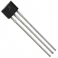
3-pin SIP,
matrix HD style
(suffix UA)
3-pin SIP,
chopper style
(suffix UA)
Two package styles provide magnetically optimized packages
for most applications. Package type LH is a modified 3-pin
SOT23W surface-mount package, while UA is a three-pin
ultra-mini SIP for through-hole mounting. Both packages are
lead (Pb) free, with 100% matte-tin-plated leadframes.
FUNCTIONAL BLOCK DIAGRAM
VCC
Amp
Sample and Hold
Dynamic Offset
Cancellation
Regulator
Low-Pass
Filter
To All Subcircuits
VOUT
Control
Current Limit
GND
A1220-DS, Rev. 19
MCO-0000309
September 22, 2017
�A1220, A1221,
A1222, and A1223
Chopper-Stabilized Precision Hall-Effect Latches
SELECTION GUIDE
Part Number
Packing [1]
Mounting
A1220ELHLX-T
13-in. reel, 10000 pieces/reel
A1220ELHLT-T [2]
7-in. reel, 3000 pieces/reel
3-pin SOT23W surface mount
A1220EUA-T [3]
Bulk, 500 pieces/bag
3-pin SIP through hole
A1220LLHLX-T
13-in. reel, 10000 pieces/reel
3-pin SOT23W surface mount
A1220LLHLT-T [2]
7-in. reel, 3000 pieces/reel
3-pin SOT23W surface mount
A1220LUA-T [3]
Bulk, 500 pieces/bag
3-pin SIP through hole
A1221ELHLX-T
13-in. reel, 10000 pieces/reel
3-pin SOT23W surface mount
A1221ELHLT-T
7-in. reel, 3000 pieces/reel
3-pin SOT23W surface mount
A1221EUA-T [3]
Bulk, 500 pieces/bag
3-pin SIP through hole
A1221LLHLX-T
13-in. reel, 10000 pieces/reel
3-pin SOT23W surface mount
A1221LLHLT-T [2]
7-in. reel, 3000 pieces/reel
3-pin SOT23W surface mount
A1221LUA-T [3]
Bulk, 500 pieces/bag
3-pin SIP through hole
[2]
Ambient, TA
BRP (Min)
BOP (Max)
–40 G
40 G
–90 G
90 G
–150 G
150 G
–180 G
180 G
3-pin SOT23W surface mount
A1222ELHLT-T
7-in. reel, 3000 pieces/reel
3-pin SOT23W surface mount
A1222ELHLX-T [2]
13-in. reel, 10000 pieces/reel
3-pin SOT23W surface mount
A1222EUA-T
Bulk, 500 pieces/bag
3-pin SIP through hole
A1222LLHLT-T
7-in. reel, 3000 pieces/reel
3-pin SOT23W surface mount
A1222LLHLX-T [2]
13-in. reel, 10000 pieces/reel
3-pin SOT23W surface mount
A1222LUA-T
Bulk, 500 pieces/bag
3-pin SIP through hole
A1223ELHLT-T
7-in. reel, 3000 pieces/reel
3-pin SOT23W surface mount
A1223ELHLX-T [2]
13-in. reel, 10000 pieces/reel
3-pin SOT23W surface mount
A1223EUA-T
Bulk, 500 pieces/bag
3-pin SIP through hole
A1223LLHLT-T
7-in. reel, 3000 pieces/reel
3-pin SOT23W surface mount
A1223LLHLX-T [2]
13-in. reel, 10000 pieces/reel
3-pin SOT23W surface mount
A1223LUA-T
Bulk, 500 pieces/bag
3-pin SIP through hole
–40°C to 85°C
–40°C to 150°C
–40°C to 85°C
–40°C to 150°C
–40°C to 85°C
–40°C to 150°C
–40°C to 85°C
–40°C to 150°C
[1] Contact Allegro
for additional packing options.
through authorized Allegro distributors only.
[3] The chopper-style UA package is not for new design; the matrix HD style UA package is recommended for new designs.
[2] Available
RoHS
COMPLIANT
Allegro MicroSystems, LLC
115 Northeast Cutoff
Worcester, Massachusetts 01615-0036 U.S.A.
1.508.853.5000; www.allegromicro.com
2
�A1220, A1221,
A1222, and A1223
Chopper-Stabilized Precision Hall-Effect Latches
ABSOLUTE MAXIMUM RATINGS
Characteristic
Forward Supply Voltage
Symbol
Notes
Rating
Units
VCC
26.5
V
Reverse Supply Voltage [1]
VRCC
–30
V
Output Off Voltage [1]
VOUT
26
V
Continuous Output Current
IOUT
25
mA
Reverse Output Current
IROUT
[1]
Operating Ambient Temperature
TA
Maximum Junction Temperature
TJ(max)
Storage Temperature
–50
mA
Range E
–40 to 85
°C
Range L
–40 to 150
°C
165
°C
175
°C
–65 to 170
°C
For 500 hours
Tstg
[1] This
rating does not apply to extremely short voltage transients such as Load Dump and/or ESD. Those events have individual
ratings, specific to the respective transient voltage event.
GND
PINOUT DIAGRAMS AND TERMINAL LIST TABLE
3
1
2
3
GND
VOUT
2
VCC
1
VOUT
Package UA
VCC
Package LH
Terminal List
Name
Description
Number
Package LH
Package UA
Connects power supply to chip
1
1
VOUT
Output from circuit
2
3
GND
Ground
3
2
VCC
Allegro MicroSystems, LLC
115 Northeast Cutoff
Worcester, Massachusetts 01615-0036 U.S.A.
1.508.853.5000; www.allegromicro.com
3
�A1220, A1221,
A1222, and A1223
Chopper-Stabilized Precision Hall-Effect Latches
ELECTRICAL CHARACTERISTICS: Valid over full operating voltage and ambient temperature ranges, unless otherwise noted
Characteristics
Symbol
Test Conditions
Min.
Typ. [1]
Max.
Unit [2]
ELECTRICAL CHARACTERISTICS
Forward Supply Voltage
VCC
Operating, TJ < 165°C
3
–
24
V
Output Leakage Current
IOUTOFF
VOUT = 24 V, B < BRP
–
–
10
µA
VOUT(SAT)
Output Saturation Voltage
IOUT = 20 mA, B > BOP
–
185
500
mV
Output Current Limit
IOM
B > BOP
30
–
60
mA
Power-On Time [3]
tPO
VCC > 3.0 V, B < BRP(min) – 10 G,
B > BOP(max) + 10 G
–
–
25
µs
Chopping Frequency
fC
–
800
–
kHz
Output Rise Time [3][4]
tr
RL = 820 Ω, CL = 20 pF
–
0.2
2
µs
tf
Output Fall Time [3][4]
Supply Current
Reverse Supply Current
RL = 820 Ω, CL = 20 pF
–
0.1
2
µs
ICC(ON)
B > BOP, VCC = 12 V
–
–
4
mA
ICC(OFF)
B < BRP, VCC = 12 V
–
–
4
mA
VRCC = –20 V
–
–
–5
mA
IRCC
Supply Zener Clamp Voltage
VZ
ICC = 5 mA; TA = 25°C
28
–
–
V
Zener Impedance
IZ
ICC = 5 mA; TA = 25°C
–
50
–
Ω
MAGNETIC CHARACTERISTICS
Operate Point
Release Point
Hysteresis
BOP
BRP
BHYS
A1220
5
22
40
G
A1221
15
50
90
G
A1222
70
110
150
G
A1223
100
150
180
G
A1220
–40
–23
–5
G
A1221
–90
–50
–15
G
A1222
–150
–110
–70
G
A1223
–180
–150
–100
G
A1220
10
45
80
G
A1221
30
100
180
G
A1222
(BOP – BRP)
A1223
140
220
300
G
200
300
360
G
[1] Typical
data are are at TA = 25°C and VCC = 12 V, and are for initial design estimations only.
G (gauss) = 0.1 mT (millitesla).
[3] Guaranteed by device design and characterization.
[4] C = oscilloscope probe capacitance.
L
[2] 1
Allegro MicroSystems, LLC
115 Northeast Cutoff
Worcester, Massachusetts 01615-0036 U.S.A.
1.508.853.5000; www.allegromicro.com
4
�A1220, A1221,
A1222, and A1223
Chopper-Stabilized Precision Hall-Effect Latches
THERMAL CHARACTERISTICS: May require derating at maximum conditions; see application information
Characteristic
Symbol
Test Conditions
Package LH, 1-layer PCB with copper limited to solder pads
Package LH, 2-layer PCB with 0.463
connected by thermal vias
RθJA
Package Thermal Resistance
in.2
of copper area each side
Maximum Allowable VCC (V)
Package UA, 1-layer PCB with copper limited to solder pads
Value
Units
228
°C/W
110
°C/W
165
°C/W
Power Derating Curve
TJ(max) = 165ºC; ICC = ICC(max)
25
24
23
22
21
20
19
18
17
16
15
14
13
12
11
10
9
8
7
6
5
4
3
2
VCC(max)
Package LH, 2-layer PCB
(RθJA = 110 ºC/W)
Package UA, 1-layer PCB
(RθJA = 165 ºC/W)
Package LH, 1-layer PCB
(RθJA = 228 ºC/W)
VCC(min)
20
40
60
80
100
120
140
160
180
Power Dissipation, PD (mW)
Temperature (ºC)
Power Dissipation versus Ambient Temperature
1900
1800
1700
1600
1500
1400
1300
1200
1100
1000
900
800
700
600
500
400
300
200
100
0
Pa
(R cka
ge
θJ
A =
L
11 H, 2
0 º -la
Pac
C/ ye
W
(R kage
) r PC
UA
θJA =
B
165 , 1-la
ºC/ yer
W)
PC
B
Pac
k
(R age LH
,
θJA =
228 1-laye
ºC/W r PC
B
)
20
40
60
80
100
120
Temperature (°C)
140
160
180
Allegro MicroSystems, LLC
115 Northeast Cutoff
Worcester, Massachusetts 01615-0036 U.S.A.
1.508.853.5000; www.allegromicro.com
5
�A1220, A1221,
A1222, and A1223
Chopper-Stabilized Precision Hall-Effect Latches
CHARACTERISTIC PERFORMANCE
6.0
5.5
5.0
4.5
4.0
3.5
3.0
2.5
2.0
1.5
1.0
0.5
0.0
Average Supply Current (On) versus Temperature
Average Supply Current (On) versus Supply Voltage
6.0
5.5
5.0
3.0V
3.8V
4.2V
12V
24V
4.5
Icc(AV)(mA)
ICC(AV) (mA)
A1220, A1221, A1222, and A1223 Electrical Characteristics
4.0
150°C
25°C
-40°C
3.5
3.0
2.5
2.0
1.5
1.0
0.5
0.0
-60
-40
-20
0
20
40
60
80
2
100 120 140 160
6
10
14
6.0
5.5
5.0
4.5
4.0
3.5
3.0
2.5
2.0
1.5
1.0
0.5
0.0
22
26
Average Supply Current (Off) versus Supply Voltage
6.0
5.5
5.0
4.5
3.0V
3.8V
4.2V
12V
24V
Icc(AV)(mA)
ICC(AV) (mA)
Average Supply Current (Off) versus Temperature
4.0
150°C
25°C
-40°C
3.5
3.0
2.5
2.0
1.5
1.0
0.5
0.0
-60 -40 -20
0
20
40
60
80
2
100 120 140 160
6
10
14
18
22
26
VCC (V)
TA (°C)
Saturation Voltage versus Temperature
Saturation Voltage versus Supply Voltage
300
300
250
250
2.6V
3.0V
3.8V
4.2V
12V
24V
200
150
100
50
VOUT(SAT) (mV)
VOUT(SAT) (mV)
18
VCC (V)
TA (°C)
200
150°C
25°C
-40°C
150
100
50
0
0
-60
-40
-20
0
20
40
60
TA (°C)
80
100 120 140 160
0
2
4
6
8
10
12
14
16
18
20
22
24
26
VCC (V)
Allegro MicroSystems, LLC
115 Northeast Cutoff
Worcester, Massachusetts 01615-0036 U.S.A.
1.508.853.5000; www.allegromicro.com
6
�A1220, A1221,
A1222, and A1223
Chopper-Stabilized Precision Hall-Effect Latches
A1220 Magnetic Characteristics
Operate Point versus Supply Voltage
Operate Point versus Temperature
40
40
35
35
BOP (G)
30
25
20
15
30
BOP (G)
(V)
3.0
3.8
4.2
12
24
(°C)
-40
25
150
25
20
15
10
10
5
5
0
0
-60
-40
-20
0
20
40
60
80
2
100 120 140 160
6
10
0
-5
-5
(V)
3.0
3.8
4.2
12
24
-15
-20
-25
-30
BRP (G)
BRP (G)
22
26
-10
-10
-15
(°C)
-40
25
150
-20
-25
-30
-35
-35
-60
-40
-20
0
20
40 60
TA (°C)
80
-40
100 120 140 160
2
Switchpoint Hysteresis versus Temperature
80
75
70
65
60
55
50
45
40
35
30
25
20
15
10
5
0
(V)
3.0
3.8
4.2
12
24
-60
-40
-20
0
20
40
60
TA (°C)
80
100 120 140 160
6
10
14
VCC (V)
18
22
26
Switchpoint Hysteresis versus Supply Voltage
BHYS (G)
BHYS (G)
18
Release Point versus Supply Voltage
Release Point versus Temperature
0
-40
14
VCC (V)
TA (°C)
80
75
70
65
60
55
50
45
40
35
30
25
20
15
10
5
0
(°C)
-40
25
150
2
6
10
14
18
22
26
VCC (V)
Allegro MicroSystems, LLC
115 Northeast Cutoff
Worcester, Massachusetts 01615-0036 U.S.A.
1.508.853.5000; www.allegromicro.com
7
�A1220, A1221,
A1222, and A1223
Chopper-Stabilized Precision Hall-Effect Latches
A1221 Magnetic Characteristics
Operate Point versus Supply Voltage
Operate Point versus Temperature
90
90
80
80
70
70
(V)
2.6
12
24
50
40
30
60
BOP (G)
BOP (G)
60
(°C)
-40
25
150
50
40
30
20
20
10
10
0
0
-60
-40
-20
0
20
40
60
80
2
100 120 140 160
6
10
18
22
26
Release Point versus Supply Voltage
Release Point versus Temperature
0
0
-10
-10
-20
-20
(V)
2.6
12
24
-40
-50
-60
-30
BRP (G)
-30
BRP (G)
14
VCC (V)
TA (°C)
-50
-60
-70
-70
-80
-80
-90
(°C)
-40
25
150
-40
-90
-60
-40
-20
0
20
40 60
TA (°C)
80
100 120 140 160
2
Switchpoint Hysteresis versus Temperature
BHYS (G)
(V)
2.6
12
24
-60
-40
-20
0
20
40
60
TA (°C)
80
100 120 140 160
10
14
VCC (V)
18
22
26
Switchpoint Hysteresis versus Supply Voltage
180
170
160
150
140
130
120
110
100
90
80
70
60
50
40
30
(°C)
-40
25
150
BHYS (G)
180
170
160
150
140
130
120
110
100
90
80
70
60
50
40
30
6
2
6
10
14
18
22
26
VCC (V)
Allegro MicroSystems, LLC
115 Northeast Cutoff
Worcester, Massachusetts 01615-0036 U.S.A.
1.508.853.5000; www.allegromicro.com
8
�A1220, A1221,
A1222, and A1223
Chopper-Stabilized Precision Hall-Effect Latches
A1222 Magnetic Characteristics
Operate Point versus Supply Voltage
Operate Point versus Temperature
150
180
140
170
160
150
120
(V)
2.6
24
110
100
140
130
120
110
100
90
90
80
70
-60
(°C)
-40
25
150
BOP (G)
BOP (G)
130
80
70
-40
-20
0
20
40
60
80
2
100 120 140 160
6
10
-70
-70
-80
-80
-120
-110
(°C)
-40
25
150
BRP (G)
(V)
2.6
24
-110
-120
-130
-140
-130
-150
-140
-170
-160
-180
-150
-40
-20
0
20
40 60
TA (°C)
80
100 120 140 160
2
Switchpoint Hysteresis versus Temperature
280
260
260
240
BHYS (G)
(V)
2.6
24
220
200
160
140
20
40
60
TA (°C)
80
100 120 140 160
22
26
(°C)
-40
25
150
200
160
0
18
220
180
-20
14
VCC (V)
240
180
-40
10
Switchpoint Hysteresis versus Supply Voltage
300
280
6
BHYS (G)
BRP (G)
26
-100
-100
140
-60
22
-90
-90
300
18
Release Point versus Supply Voltage
Release Point versus Temperature
-60
14
VCC (V)
TA (°C)
2
6
10
14
18
22
26
VCC (V)
Allegro MicroSystems, LLC
115 Northeast Cutoff
Worcester, Massachusetts 01615-0036 U.S.A.
1.508.853.5000; www.allegromicro.com
9
�A1220, A1221,
A1222, and A1223
Chopper-Stabilized Precision Hall-Effect Latches
FUNCTIONAL DESCRIPTION
OPERATION
The output of these devices switches low (turns on) when a magnetic field perpendicular to the Hall element exceeds the operate
point threshold, BOP (see panel A of figure 1). After turn-on, the
output voltage is VOUT(SAT) . The output transistor is capable of
sinking current up to the short circuit current limit, IOM, which is
a minimum of 30 mA. When the magnetic field is reduced below
the release point, BRP , the device output goes high (turns off).
The difference in the magnetic operate and release points is the
hysteresis, BHYS , of the device. This built-in hysteresis allows
clean switching of the output even in the presence of external
mechanical vibration and electrical noise.
Removal of the magnetic field will leave the device output
latched on if the last crossed switchpoint is BOP, or latched off if
the last crossed switch point is BRP.
Powering-on the device in the hysteresis range (less than BOP and
higher than BRP) will give an indeterminate output state. The correct state is attained after the first excursion beyond BOP or BRP .
FUNCTIONAL SAFETY
2
-
The A1220, A1221, A1222, and A1223 comply
with the international standard for automotive
functional safety, ISO 26262, as Quality Managed (QM) products. The devices are each classified as a SEooC
APPLICATIONS
It is strongly recommended that an external bypass capacitor be
connected (in close proximity to the Hall element) between the
supply and ground of the device to reduce both external noise
and noise generated by the chopper stabilization technique. As is
shown in panel B of figure 1, a 0.1 µF capacitor is typical.
Extensive applications information for Hall effect devices is
available in:
• Hall-Effect IC Applications Guide, Application Note 27701
• Guidelines for Designing Subassemblies Using Hall-Effect
Devices, Application Note 27703.1
• Soldering Methods for Allegro’s Products – SMT and ThroughHole, Application Note 26009
All are provided in Allegro Electronic Data Book, AMS-702, and
the Allegro Web site, www.allegromicro.com.
VS
V+
VOUT
Switch to High
VCC
Switch to Low
VCC
CBYP
0.1 µF
VOUT(SAT)
0
BOP
B–
BRP
0
(Safety Element out of Context) and can be easily integrated into
safety-critical systems requiring higher ASIL ratings that incorporate external diagnostics or use measures such as redundancy.
Safety documentation will be provided to support and guide the
integration process. For further information, contact your local
Allegro field applications engineer or sales representative.
A122x
VOUT
RL
Output
GND
B+
BHYS
(A)
(B)
Figure 1. Switching behavior of latches. In panel A, on the horizontal axis, the B+ direction indicates increasing south polarity magnetic field strength,
and the B– direction indicates decreasing south polarity field strength (including the case of increasing north polarity). This behavior can be exhibited
when using a circuit such as that shown in panel B.
Allegro MicroSystems, LLC
115 Northeast Cutoff
Worcester, Massachusetts 01615-0036 U.S.A.
1.508.853.5000; www.allegromicro.com
10
�A1220, A1221,
A1222, and A1223
Chopper-Stabilized Precision Hall-Effect Latches
CHOPPER STABILIZATION TECHNIQUE
When using Hall effect technology, a limiting factor for
switchpoint accuracy is the small signal voltage developed across
the Hall element. This voltage is disproportionally small relative
to the offset that can be produced at the output of the Hall element. This makes it difficult to process the signal while maintaining an accurate, reliable output over the specified operating
temperature and voltage ranges.
Chopper stabilization is a unique approach used to minimize
Hall offset on the chip. The Allegro technique, namely Dynamic
Quadrature Offset Cancellation, removes key sources of the output drift induced by thermal and mechanical stresses. This offset
reduction technique is based on a signal modulation-demodulation process. The undesired offset signal is separated from the
magnetic field-induced signal in the frequency domain, through
modulation. The subsequent demodulation acts as a modulation
process for the offset, causing the magnetic field induced signal
to recover its original spectrum at baseband, while the dc offset
becomes a high-frequency signal. The magnetic sourced signal
then can pass through a low-pass filter, while the modulated DC
offset is suppressed. This configuration is illustrated in figure 2.
The chopper stabilization technique uses a 400 kHz high frequency clock. For demodulation process, a sample and hold
technique is used, where the sampling is performed at twice the
chopper frequency (800 kHz). This high-frequency operation
allows a greater sampling rate, which results in higher accuracy
and faster signal-processing capability. This approach desensitizes the chip to the effects of thermal and mechanical stresses,
and produces devices that have extremely stable quiescent Hall
output voltages and precise recoverability after temperature
cycling. This technique is made possible through the use of a
BiCMOS process, which allows the use of low-offset, low-noise
amplifiers in combination with high-density logic integration and
sample-and-hold circuits.
The repeatability of magnetic field-induced switching is affected
slightly by a chopper technique. However, the Allegro high
frequency chopping approach minimizes the affect of jitter and
makes it imperceptible in most applications. Applications that are
more likely to be sensitive to such degradation are those requiring
precise sensing of alternating magnetic fields; for example, speed
sensing of ring-magnet targets. For such applications, Allegro
recommends its digital device families with lower sensitivity
to jitter. For more information on those devices, contact your
Allegro sales representative.
Regulator
Hall Element
Amp
Sample and
Hold
Clock/Logic
Low-Pass
Filter
Figure 2. Model of chopper stabilization technique
Allegro MicroSystems, LLC
115 Northeast Cutoff
Worcester, Massachusetts 01615-0036 U.S.A.
1.508.853.5000; www.allegromicro.com
11
�A1220, A1221,
A1222, and A1223
Chopper-Stabilized Precision Hall-Effect Latches
POWER DERATING
The device must be operated below the maximum junction
temperature of the device, TJ(max). Under certain combinations of
peak conditions, reliable operation may require derating supplied
power or improving the heat dissipation properties of the application. This section presents a procedure for correlating factors
affecting operating TJ. (Thermal data is also available on the
Allegro MicroSystems website.)
The Package Thermal Resistance, RθJA, is a figure of merit summarizing the ability of the application and the device to dissipate
heat from the junction (die), through all paths to the ambient air.
Its primary component is the Effective Thermal Conductivity, K,
of the printed circuit board, including adjacent devices and traces.
Radiation from the die through the device case, RθJC, is relatively
small component of RθJA. Ambient air temperature, TA, and air
motion are significant external factors, damped by overmolding.
The effect of varying power levels (Power Dissipation, PD), can
be estimated. The following formulas represent the fundamental
relationships used to estimate TJ, at PD.
PD = VIN × IIN
(1)
ΔT = PD × RθJA
(2)
TJ = TA + ΔT
(3)
Example: Reliability for VCC at TA = 150°C, package LH, using a
minimum-K PCB.
Observe the worst-case ratings for the device, specifically:
RθJA = 228°C/W, TJ(max) = 165°C, VCC(max) = 24 V, and
ICC(max) = 4 mA.
Calculate the maximum allowable power level, PD(max). First,
invert equation 3:
ΔTmax = TJ(max) – TA = 165°C – 150°C = 15°C
This provides the allowable increase to TJ resulting from internal
power dissipation. Then, invert equation 2:
PD(max) = ΔTmax ÷ RθJA = 15°C ÷ 228°C/W = 66 mW
Finally, invert equation 1 with respect to voltage:
VCC(est) = PD(max) ÷ ICC(max) = 66 mW ÷ 4 mA = 16.4 V
The result indicates that, at TA, the application and device can
dissipate adequate amounts of heat at voltages ≤VCC(est).
Compare VCC(est) to VCC(max). If VCC(est) ≤ VCC(max), then reliable operation between VCC(est) and VCC(max) requires enhanced
RθJA. If VCC(est) ≥ VCC(max), then operation between VCC(est)
and VCC(max) is reliable under these conditions.
For example, given common conditions such as: TA= 25°C,
VCC = 12 V, ICC = 1.6 mA, and RθJA = 165°C/W, then:
PD = VCC × ICC = 12 V × 1.6 mA = 19 mW
ΔT = PD × RθJA = 19 mW × 165°C/W = 3°C
TJ = TA + ΔT = 25°C + 3°C = 28°C
A worst-case estimate, PD(max), represents the maximum allowable power level (VCC(max), ICC(max)), without exceeding TJ(max),
at a selected RθJA and TA.
Allegro MicroSystems, LLC
115 Northeast Cutoff
Worcester, Massachusetts 01615-0036 U.S.A.
1.508.853.5000; www.allegromicro.com
12
�A1220, A1221,
A1222, and A1223
Chopper-Stabilized Precision Hall-Effect Latches
Package LH, 3-Pin (SOT-23W)
+0.12
2.98 –0.08
1.49 D
4°±4°
3
A
+0.020
0.180–0.053
0.96 D
+0.10
2.90 –0.20
+0.19
1.91 –0.06
2.40
0.70
D
0.25 MIN
1.00
2
1
0.55 REF
0.25 BSC
0.95
Seating Plane
Gauge Plane
8 × 10°
B
PCB Layout Reference View
Branded Face
1.00 ±0.13
0.95 BSC
Active Area Depth, 0.28 mm REF
B
Reference land pattern layout
All pads a minimum of 0.20 mm from all adjacent pads; adjust as necessary
to meet application process requirements and PCB layout tolerances
Branding scale and appearance at supplier discretion
Hall element, not to scale
NNT
0.40 ±0.10
A
D
Standard Branding Reference View
+0.10
0.05 –0.05
For Reference Only; not for tooling use (reference dwg. 802840)
Dimensions in millimeters
Dimensions exclusive of mold flash, gate burrs, and dambar protrusions
Exact case and lead configuration at supplier discretion within limits shown
C
C
1
N = Last two digits of device part number
T = Temperature code (letter)
NNN
1
N = Last three digits of device part number
Allegro MicroSystems, LLC
115 Northeast Cutoff
Worcester, Massachusetts 01615-0036 U.S.A.
1.508.853.5000; www.allegromicro.com
13
�A1220, A1221,
A1222, and A1223
Chopper-Stabilized Precision Hall-Effect Latches
Package UA, 3-Pin SIP, Matrix HD Style
+0.08
4.09 –0.05
45°
B
E
C
2.04
1.52 ±0.05
+0.08
3.02 –0.05
1.44
E
10°
Mold Ejector
Pin Indent
E
Branded
Face
A
1.02
MAX
45°
0.79 REF
NNN
1
2
1
3
D Standard Branding Reference View
= Supplier emblem
N = Last three digits of device part number
+0.03
0.41 –0.06
14.99 ±0.25
+0.05
0.43 –0.07
For Reference Only; not for tooling use (reference DWG-9065)
Dimensions in millimeters
Dimensions exclusive of mold flash, gate burrs, and dambar protrusions
Exact case and lead configuration at supplier discretion within limits shown
A
Dambar removal protrusion (6X)
B
Gate and tie bar burr area
C
Active Area Depth, 0.50 mm REF
D
Branding scale and appearance at supplier discretion
E
Hall element (not to scale)
1.27 NOM
Allegro MicroSystems, LLC
115 Northeast Cutoff
Worcester, Massachusetts 01615-0036 U.S.A.
1.508.853.5000; www.allegromicro.com
14
�A1220, A1221,
A1222, and A1223
Chopper-Stabilized Precision Hall-Effect Latches
Package UA, 3-Pin SIP, Chopper Style
+0.08
4.09 –0.05
45°
B
C
E
2.04
1.52 ±0.05
1.44 E
Mold Ejector
Pin Indent
+0.08
3.02 –0.05
E
Branded
Face
45°
1
2.16
MAX
D Standard Branding Reference View
0.79 REF
0.51
REF
NNT
NOT FOR
NEW DESIGN
A
1
2
3
+0.03
0.41 –0.06
15.75 ±0.51
= Supplier emblem
N = Last two digits of device part number
T = Temperature code
For Reference Only; not for tooling use (reference DWG-9049)
Dimensions in millimeters
Dimensions exclusive of mold flash, gate burrs, and dambar protrusions
Exact case and lead configuration at supplier discretion within limits shown
A
Dambar removal protrusion (6X)
B Gate burr area
C Active Area Depth, 0.50 mm REF
+0.05
0.43 –0.07
D
Branding scale and appearance at supplier discretion
E
Hall element, not to scale
1.27 NOM
Allegro MicroSystems, LLC
115 Northeast Cutoff
Worcester, Massachusetts 01615-0036 U.S.A.
1.508.853.5000; www.allegromicro.com
15
�A1220, A1221,
A1222, and A1223
Chopper-Stabilized Precision Hall-Effect Latches
Revision History
Number
Date
Description
15
September 16, 2013
Update UA package drawing
16
September 21, 2015
Added AEC-Q100 qualification under Features and Benefits
17
January 12, 2016
18
October 20, 2016
19
September 22, 2017
Updated Reverse Supply Current test conditions in Electrical Characteristics table
Chopper-style UA package designated as not for new design
Updated Maximum Junction Temperature in Absolute Maximum Ratings table and
Figure 1B; added Functional Safety information
Copyright ©2017, Allegro MicroSystems, LLC
Allegro MicroSystems, LLC reserves the right to make, from time to time, such departures from the detail specifications as may be required to
permit improvements in the performance, reliability, or manufacturability of its products. Before placing an order, the user is cautioned to verify that
the information being relied upon is current.
Allegro’s products are not to be used in any devices or systems, including but not limited to life support devices or systems, in which a failure of
Allegro’s product can reasonably be expected to cause bodily harm.
The information included herein is believed to be accurate and reliable. However, Allegro MicroSystems, LLC assumes no responsibility for its
use; nor for any infringement of patents or other rights of third parties which may result from its use.
For the latest version of this document, visit our website:
www.allegromicro.com
Allegro MicroSystems, LLC
115 Northeast Cutoff
Worcester, Massachusetts 01615-0036 U.S.A.
1.508.853.5000; www.allegromicro.com
16
�