A1250
Hall-Effect Latch / Bipolar Switch
FEATURES AND BENEFITS
DESCRIPTION
Packages:
The A1250 includes the following on a single silicon chip:
a voltage regulator, Hall-voltage generator, small-signal
amplifier, chopper stabilization, Schmitt trigger, and a shortcircuit-protected open-drain output. Advanced BiCMOS
wafer fabrication processing takes advantage of low-voltage
requirements, component matching, very low input-offset
errors, and small component geometries.
•
•
•
•
•
•
AEC-Q100 automotive qualified
High-speed, 4-phase chopper stabilization
Low operating voltage down to 3 V
High sensitivity
Stable switchpoints
Robust EMC
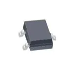
3-Pin SOT23W
(suffix LH)
The A1250 Hall-effect sensor IC is a temperature-stable,
stress-resistant bipolar switch. This device is the most sensitive
Hall-effect device in the Allegro™ bipolar switch family and is
intended for ring-magnet sensing. Superior high-temperature
performance is made possible through an Allegro patented
dynamic offset cancellation that utilizes chopper stabilization.
This method reduces the offset voltage normally caused by
device overmolding, temperature dependencies, and thermal
stress.
3-Pin SIP
(suffix UA)
The A1250 Hall-effect bipolar switch turns on in a south
polarity magnetic field of sufficient strength and switches
off in a north polarity magnetic field of sufficient strength.
Because the output state is not defined if the magnetic field
is diminished or removed, to ensure that the device switches,
Allegro recommends using magnets of both polarities and of
sufficient strength in the application.
Not to scale
The A1250 is rated for operation in the ambient temperature
Continued on the next page…
V+
Regulator
To All Subcircuits
VCC
Amp
Sample and Hold
Dynamic Offset
Cancellation
Clock / Logic
Low-Pass
Filter
VOUT
Control
Current
Limit
1Ω
GND
Functional Block Diagram
A1250-DS, Rev. 4
�A1250
Hall-Effect Latch / Bipolar Switch
Description (continued)
range L, –40°C to 150°C. Two package styles provide magnetically
optimized solutions for most applications. Each package is lead (Pb)
free version, with 100% matte-tin-plated leadframe.
SPECIFICATIONS
Selection Guide
Part Number
Packing*
Mounting
A1250LLHLT-T
7-in. reel, 3000 pieces/reel
Surface mount
A1250LLHLX-T
13-in. reel, 10 000 pieces/reel
Surface mount
A1250LUA-T
Bulk, 500 pieces/bag
SIP through hole
*Contact Allegro
Ambient, TA
(°C)
–40 to 150
for additional packing options.
Absolute Maximum Ratings
Characteristic
Symbol
Notes
Rating
Unit*
Forward Supply Voltage
VCC
28
V
Reverse Supply Voltage
VRCC
–18
V
Output Off Voltage
VOUT
28
V
Reverse Output Voltage
VROUT
–0.6
V
IOUTSINK
Internally limited
A
IROUT
–10
mA
Output Current
Reverse Output Current
Magnetic Flux Density
B
Operating Ambient Temperature
TA
Maximum Junction Temperature
Storage Temperature
Unlimited
G
–40 to 150
ºC
TJ(max)
165
ºC
Tstg
–65 to 170
ºC
Range L
*1 G (gauss) = 0.1 mT (millitesla).
Pin-Out Diagrams and Terminal List Table
GND
Terminal List Table
3
2
3
VOUT
VOUT
Package LH
1
GND
2
VCC
1
VCC
Number
Package UA
Name
Package
LH
Package
UA
Function
VCC
1
1
Device supply
VOUT
2
3
Device output
GND
3
2
Ground
Allegro MicroSystems, LLC
115 Northeast Cutoff
Worcester, Massachusetts 01615-0036 U.S.A.
1.508.853.5000; www.allegromicro.com
2
�A1250
Hall-Effect Latch / Bipolar Switch
OPERATING CHARACTERISTICS: valid at TA = –40°C to 150°C, CBYPASS = 0.1 µF, unless otherwise noted
Characteristic
Symbol
Test Conditions
Min.
Typ.
Max.
Unit
ELECTRICAL CHARACTERISTICS
Supply Voltage
Output Leakage Current
Output On Voltage
VCC
Operating TJ < 165°C
3.0
–
24
V
IOUTOFF
VOUT = 24 V, B < BRP
–
–
10
µA
VOUT(SAT)
IOUT = 20 mA, B > BOP
–
–
500
mV
Output Current Limit
IOM
B > BOP
30
–
60
mA
Power-On Time
tPO
VCC > 3.0 V
–
–
25
µs
Chopping Frequency
fc
–
160
–
kHz
Output Rise Time1
tr
RLOAD = 820 Ω, CS = 20 pF
–
–
2
µs
tf
Output Fall
Time1
Supply Current
Reverse Battery Current
RLOAD = 820 Ω, CS = 20 pF
–
–
2
µs
ICCON
B > BOP
–
–
4
mA
ICCOFF
B < BRP
–
–
4
mA
VRCC = –18 V
–
–
–2
mA
IRCC
Supply Zener Clamp Voltage
VZ
ICC = 6.5 mA, TA = 25°C
28
–
–
V
Supply Zener Current
IZ
VCC = 28 V
–
–
7
mA
MAGNETIC CHARACTERISTICS2: valid at TA = –40°C to 150°C, TJ ≤ TJ(max), unless otherwise noted
Operate Point
BOP
–10
5
25
G
Release Point
BRP
–25
–5
10
G
Hysteresis
BHYS
5
10
25
G
1Guaranteed
by design.
2Magnetic flux density, B, is indicated as negative value for north-polarity fields, and positive for south-polarity fields.
Allegro MicroSystems, LLC
115 Northeast Cutoff
Worcester, Massachusetts 01615-0036 U.S.A.
1.508.853.5000; www.allegromicro.com
3
�A1250
Hall-Effect Latch / Bipolar Switch
THERMAL CHARACTERISTICS: may require derating at maximum conditions; see application information
Characteristic
Symbol
Package Thermal Resistance
Test Conditions*
RθJA
Value
Units
Package LH, 1-layer PCB with copper limited to solder pads
228
ºC/W
Package LH, 2-layer PCB with 0.463 in.2 of copper area each side
connected by thermal vias
110
ºC/W
Package UA, 1-layer PCB with copper limited to solder pads
165
ºC/W
*Additional thermal information available on Allegro Web site.
Maximum Allowable VCC (V)
Power Derating Curve
25
24
23
22
21
20
19
18
17
16
15
14
13
12
11
10
9
8
7
6
5
4
3
2
VCC(max)
2-layer PCB, Package LH
(RθJA = 110 ºC/W)
1-layer PCB, Package UA
(RθJA = 165 ºC/W)
1-layer PCB, Package LH
(RθJA = 228 ºC/W)
VCC(min)
20
40
60
80
100
120
140
160
180
Temperature (ºC)
Power Dissipation, PD (m W)
Power Dissipation versus Ambient Temperature
1900
1800
1700
1600
1500
1400
1300
1200
1100
1000
900
800
700
600
500
400
300
200
100
0
2l
(R aye
rP
θJ
C
A =
11 B, P
0 º ac
1-la
C/ ka
W
(R yer P
) ge L
CB
θJA =
H
,
165 Pac
ºC/ kag
eU
W)
A
1-lay
er P
(R
CB,
θJA =
228 Packag
ºC/W
e LH
)
20
40
60
80
100
120
Temperature (°C)
140
160
180
Allegro MicroSystems, LLC
115 Northeast Cutoff
Worcester, Massachusetts 01615-0036 U.S.A.
1.508.853.5000; www.allegromicro.com
4
�A1250
Hall-Effect Latch / Bipolar Switch
CHARACTERISTIC PERFORMANCE DATA
Supply Current (On) versus Ambient Temperature
4.0
4.0
3.5
3.5
3.0
3.0
2.5
2.5
ICCON (mA)
ICCON (mA)
Supply Current (On) versus Supply Voltage
2.0
-40°C
1.5
2.0
1.0
1.0
150°C
0.5
0
Vcc: 24 V
Vcc: 3 V
1.5
25°C
0.5
0
5
10
15
20
0
25
-50
-25
0
25
VCC (V)
3.5
3.5
3.0
3.0
2.5
2.5
ICCOFF (mA)
4.0
2.0
1.5
-40°C
1.0
25°C
0.5
5
10
100
125
150
15
20
Vcc: 24 V
Vcc: 3 V
2.0
1.5
1.0
150°C
0
75
Supply Current (Off) versus Ambient Temperature
4.0
0.5
0
25
-50
-25
0
25
50
75
100
125
150
TA (°C)
VCC (V)
VOUT(SAT) versus Ambient Temperature
IOUT = 20 mA
500
Vcc: 3 V
Vcc: 24 V
450
400
VOUT(SAT)
ICCOFF (mA)
Supply Current (Off) versus Supply Voltage
0
50
TA (°C)
350
300
250
200
150
100
50
0
-50
-25
0
25
50
75
100
125
150
TA (°C)
Allegro MicroSystems, LLC
115 Northeast Cutoff
Worcester, Massachusetts 01615-0036 U.S.A.
1.508.853.5000; www.allegromicro.com
5
�A1250
Hall-Effect Latch / Bipolar Switch
Operate Point versus Ambient Temperature
Release Point versus Ambient Temperature
25
10
Vcc: 24 V
20
Vcc: 3 V
BRP (G)
0
10
5
-5
-10
0
-15
-5
-20
-50
-25
0
25
50
75
100
125
-25
150
-50
-25
0
TA (°C)
25
50
75
100
125
150
TA (°C)
Hysteresis versus Ambient Temperature
25
Vcc: 24 V
23
Vcc: 3 V
21
19
BOP (G)
BOP (G)
15
-10
Vcc: 24 V
5
Vcc: 3 V
17
15
13
11
9
7
5
-50
-25
0
25
50
75
100
125
150
TA (°C)
Allegro MicroSystems, LLC
115 Northeast Cutoff
Worcester, Massachusetts 01615-0036 U.S.A.
1.508.853.5000; www.allegromicro.com
6
�A1250
Hall-Effect Latch / Bipolar Switch
FUNCTIONAL DESCRIPTION
The output of this device switches low (turns on) when a magnetic
field perpendicular to the Hall sensor IC exceeds the operate point
threshold, BOP . After turn-on, the output voltage is VOUT(SAT) .
The output transistor is capable of sinking current up to the short
circuit current limit IOM , which is a minimum of 30 mA. When
the magnetic field is reduced below the release point, BRP , the
device output goes high (turns off). The difference in the magnetic
operate and release points is the hysteresis, BHYS , of the device.
This built-in hysteresis allows clean switching of the output even
in the presence of external mechanical vibration and electrical
noise.
Given the magnetic parameter specifications (refer to Magnetic
Characteristics table), bipolar switches will operate in one of three
modes, depending on switchpoints. For typical values of BOP and
BRP , the device will operate as a latch, as shown in figure 1a.
Note that, when the magnetic flux density exceeds a switchpoint,
the output will retain its state when the magnetic field is removed.
The other two modes of operation are the unipolar switch and the
(A)
negative switch, shown in panels 1b and 1c, respectively. The
unipolar switch type operates only in a south polarity field, and
will switch to the high state if the magnetic field is removed. The
negative switch operates only in a north polarity field, and will
switch to the low state if the magnetic field is removed.
Individual bipolar switch devices exhibit any one of the three
switching behaviors: latch, unipolar, or negative switch. Because
these devices are not guaranteed to behave as latches, magnetic
fields of sufficient magnitude and alternate polarity are required to
ensure output switching.
Powering up the device in the hysteresis band, that is in a magnetic field less than BOP and higher than BRP , allows an indeterminate output state. Note that this hysteresis band encompasses
zero magnetic field on devices that exhibit latch behaviors. The
correct state is determined after the first magnetic excursion
beyond BOP or BRP .
(B)
V+
(C)
V+
V+
VOUT
Switch to High
Switch to High
VOUT
B+
BHYS
B–
BRP
BRP
B– 0
VOUT(SAT)
0
BOP
BHYS
B+
VOUT(SAT)
0
BOP
0
BOP
B–
BRP
VOUT(SAT)
0
VCC
Switch to Low
Switch to Low
VOUT
VCC
Switch to Low
Switch to High
VCC
0
B+
BHYS
Figure 1: Bipolar Device Output Switching Modes
These behaviors can be exhibited when using a circuit such as that shown in figure 1. Panel A displays the hysteresis when a device exhibits
latch mode (note that the BHYS band incorporates B = 0), panel B shows unipolar switch behavior (the BHYS band is more positive than B = 0),
and panel C shows negative switch behavior (the BHYS band is more negative than B = 0). Bipolar devices, such as the A1250, can operate in
any of the three modes.
Allegro MicroSystems, LLC
115 Northeast Cutoff
Worcester, Massachusetts 01615-0036 U.S.A.
1.508.853.5000; www.allegromicro.com
7
�A1250
Hall-Effect Latch / Bipolar Switch
APPLICATION INFORMATION
V+
VCC
RLOAD
A1250
CBYPASS
0.1 µF
IC Output
VOUT
GND
Figure 2: Typical Application Circuit
Chopper Stabilization Technique
When using Hall-effect technology, a limiting factor for
switchpoint accuracy is the small signal voltage developed across
the Hall element. This voltage is disproportionally small relative
to the offset that can be produced at the output of the Hall sensor
IC. This makes it difficult to process the signal while maintaining an accurate, reliable output over the specified operating
temperature and voltage ranges. Chopper stabilization is a unique
approach used to minimize Hall offset on the chip. Allegro
employs a patented technique to remove key sources of the output drift induced by thermal and mechanical stresses. This offset
reduction technique is based on a signal modulation-demodulation process. The undesired offset signal is separated from the
magnetic field-induced signal in the frequency domain, through
modulation. The subsequent demodulation acts as a modulation
process for the offset, causing the magnetic field-induced signal
to recover its original spectrum at base band, while the DC offset
becomes a high-frequency signal. The magnetic-sourced signal
then can pass through a low-pass filter, while the modulated DC
offset is suppressed. In addition to the removal of the thermal and
stress related offset, this novel technique also reduces the amount
of thermal noise in the Hall sensor IC while completely removing
the modulated residue resulting from the chopper operation. The
chopper stabilization technique uses a high frequency sampling
clock. For demodulation process, a sample and hold technique is
used. This high-frequency operation allows a greater sampling
rate, which results in higher accuracy and faster signal-processing
capability. This approach desensitizes the chip to the effects
of thermal and mechanical stresses, and produces devices that
have extremely stable quiescent Hall output voltages and precise
recoverability after temperature cycling. This technique is made
possible through the use of a BiCMOS process, which allows the
use of low-offset, low-noise amplifiers in combination with highdensity logic integration and sample-and-hold circuits.
Regulator
Clock/Logic
Hall Element
Amp
Anit-aliasing
LP Filter
Tuned
Filter
Figure 3: Concept of Chopper Stabilization Technique
Allegro MicroSystems, LLC
115 Northeast Cutoff
Worcester, Massachusetts 01615-0036 U.S.A.
1.508.853.5000; www.allegromicro.com
8
�A1250
Hall-Effect Latch / Bipolar Switch
POWER DERATING
The device must be operated below the maximum junction
temperature of the device, TJ(max) . Under certain combinations of peak conditions, reliable operation may require derating
supplied power or improving the heat dissipation properties of
the application. This section presents a procedure for correlating
factors affecting operating TJ. (Thermal data is also available on
the Allegro MicroSystems Web site.)
The Package Thermal Resistance, RθJA, is a figure of merit summarizing the ability of the application and the device to dissipate
heat from the junction (die), through all paths to the ambient air.
Its primary component is the Effective Thermal Conductivity,
K, of the printed circuit board, including adjacent devices and
traces. Radiation from the die through the device case, RθJC, is
relatively small component of RθJA. Ambient air temperature,
TA, and air motion are significant external factors, damped by
overmolding.
The effect of varying power levels (Power Dissipation, PD), can
be estimated. The following formulas represent the fundamental
relationships used to estimate TJ, at PD.
PD = VIN × IIN (1)
ΔT = PD × RθJA (2)
TJ = TA + ΔT
For example, given common conditions such as: TA= 25°C,
VIN = 12 V, IIN = 4 mA, and RθJA = 140 °C/W, then:
(3)
A worst-case estimate, PD(max) , represents the maximum allowable power level, without exceeding TJ(max) , at a selected RθJA
and TA.
Example: Reliability for VCC at TA = 150°C, package UA, using a
single-layer PCB.
Observe the worst-case ratings for the device, specifically:
RθJA = 165 °C/W, TJ(max) = 165°C, VCC(max) = 24 V, and
ICC(max) = 4 mA.
Calculate the maximum allowable power level, PD(max) . First,
invert equation 3:
ΔTmax = TJ(max) – TA = 165 °C – 150 °C = 15 °C
This provides the allowable increase to TJ resulting from internal
power dissipation. Then, invert equation 2:
PD(max) = ΔTmax ÷ RθJA = 15°C ÷ 165 °C/W = 91 mW
Finally, invert equation 1 with respect to voltage:
VCC(est) = PD(max) ÷ ICC(max) = 91 mW ÷ 4 mA = 23 V
The result indicates that, at TA, the application and device can
dissipate adequate amounts of heat at voltages ≤VCC(est) .
Compare VCC(est) to VCC(max) . If VCC(est) ≤ VCC(max) , then
reliable operation between VCC(est) and VCC(max) requires
enhanced RθJA. If VCC(est) ≥ VCC(max) , then operation
between VCC(est) and VCC(max) is reliable under these conditions.
PD = VIN × IIN = 12 V × 4 mA = 48 mW
ΔT = PD × RθJA = 48 mW × 140 °C/W = 7°C
TJ = TA + ΔT = 25°C + 7°C = 32°C
Allegro MicroSystems, LLC
115 Northeast Cutoff
Worcester, Massachusetts 01615-0036 U.S.A.
1.508.853.5000; www.allegromicro.com
9
�A1250
Hall-Effect Latch / Bipolar Switch
PACKAGE OUTLINE DRAWINGS
For Reference Only – Not for Tooling Use
(Reference DWG-2840)
Dimensions in millimeters – NOT TO SCALE
Dimensions exclusive of mold flash, gate burrs, and dambar protrusions
Exact case and lead configuration at supplier discretion within limits shown
+0.12
2.98 –0.08
D
1.49
4°±4°
A
3
0.180
+0.020
–0.053
0.96 D
+0.10
2.90
–0.20
1.91
+0.19
–0.06
2.40
0.70
D
0.25 MIN
1.00
2
1
0.55 REF
0.25 BSC
0.95
Seating Plane
B
Gauge Plane
8X 10° REF
PCB Layout Reference View
Branded Face
1.00 ±0.13
0.05
0.95 BSC
+0.10
–0.05
NNN
C
0.40 ±0.10
Standard Branding Reference View
N = Last three digits of device part number
A Active Area Depth, 0.28 ±0.04 mm
B Reference land pattern layout
All pads a minimum of 0.20 mm from all adjacent pads; adjust as necessary
to meet application process requirements and PCB layout tolerances
C Branding scale and appearance at supplier discretion
D Hall elements, not to scale
Figure 4: Package LH, 3-Pin SOT23W
Allegro MicroSystems, LLC
115 Northeast Cutoff
Worcester, Massachusetts 01615-0036 U.S.A.
1.508.853.5000; www.allegromicro.com
10
�A1250
Hall-Effect Latch / Bipolar Switch
For Reference Only – Not for Tooling Use
(Reference DWG-9013)
Dimensions in millimeters – NOT TO SCALE
Dimensions exclusive of mold flash, gate burrs, and dambar protrusions
Exact case and lead configuration at supplier discretion within limits shown
45°
B
4.09
+0.08
–0.05
1.52 ±0.05
E
2.04
C
2 X 10°
1.44 E
3.02
E
Mold Ejector
Pin Indent
+0.08
–0.05
45°
Branded
Face
A
1.02 MAX
0.79 REF
1
2
3
0.43
+0.05
–0.07
0.41
+0.03
–0.06
1.27 NOM
NNN
14.99 ±0.25
1
D
Standard Branding Reference View
= Supplier emblem
N = Last three digits of device part number
A
Dambar removal protrusion (6X)
B
Gate and tie bar burr area
C
Active Area Depth, 0.50 mm REF
D
Branding scale and appearance at supplier discretion
E
Hall element, not to scale
Figure 5: Package UA, 3-Pin SIP
Allegro MicroSystems, LLC
115 Northeast Cutoff
Worcester, Massachusetts 01615-0036 U.S.A.
1.508.853.5000; www.allegromicro.com
11
�A1250
Hall-Effect Latch / Bipolar Switch
Revision History
Revision
Revision Date
Description of Revision
1
March 22, 2012
2
October 29, 2014
Update product selection
Corrected tolerance on Package Outline Drawing
3
February 4, 2015
Corrected dimension on Package Drawing
4
September 21, 2015
Added AEC-Q100 qualification under Features and Benefits
Copyright ©2015, Allegro MicroSystems, LLC
Allegro MicroSystems, LLC reserves the right to make, from time to time, such departures from the detail specifications as may be required to
permit improvements in the performance, reliability, or manufacturability of its products. Before placing an order, the user is cautioned to verify that
the information being relied upon is current.
Allegro’s products are not to be used in any devices or systems, including but not limited to life support devices or systems, in which a failure of
Allegro’s product can reasonably be expected to cause bodily harm.
The information included herein is believed to be accurate and reliable. However, Allegro MicroSystems, LLC assumes no responsibility for its
use; nor for any infringement of patents or other rights of third parties which may result from its use.
For the latest version of this document, visit our website:
www.allegromicro.com
Allegro MicroSystems, LLC
115 Northeast Cutoff
Worcester, Massachusetts 01615-0036 U.S.A.
1.508.853.5000; www.allegromicro.com
12
�