A1262
2D Dual-Channel Ultrasensitive Hall-Effect Latch
FEATURES AND BENEFITS
DESCRIPTION
• 2 D magnetic sensing via planar and vertical Hall elements
□□ Quadrature outputs
□□ 90° phase separation between channels
• Dual-channel output allows independent use of
Z-axis planar Hall in conjunction with vertical Hall:
□□ Y-axis (default option)
□□ X-axis (with -X option)
• High sensitivity, BOP typically 17 G
• Automotive grade
□□ AEC-Q100 qualified for use in automotive
applications (L temperature range option)
□□ Output short-circuit protection
□□ Resistant to physical stress
□□ Reverse-battery protection
□□ Superior temperature stability
□□ Supply voltage Zener clamp
• Small size
The A1262 is a two channel, latching Hall-effect sensor IC
that features both vertical and planar Hall elements. The
vertical and planar Hall elements feature sensing axes that are
orthogonal to one another and provide 90° of phase separation
for ring magnets that is inherently independent of magnet pole
spacing and air gap.
TYPICAL APPLICATIONS
Continued on the next page…
• Automotive
□□ Blower fans
□□ Electric pumps
□□ Electronic power
steering
□□ Seat motors
□□ Trunk/liftgate motors
□□ Window/sunroof
motors
• Industrial, Commercial,
and Consumer
□□ Garage doors
□□ Industrial motors
□□ Motorized window
blinds
□□ Motorized gates
□□ Pumps
□□ White goods
The 2D architecture of the A1262 simplifies the design of
motors and magnetic encoders by providing quadrature output
signals in a very small footprint. The A1262 outputs allow the
speed and direction of a rotating ring magnet to be determined.
The A1262 is available in two sensing options that allow
flexibility in end-system magnetic design. Both options
feature a planar Hall plate that is sensitive to magnetic fields
perpendicular to the face of the package (Z). Two options of
vertical Hall plate orientation (X or Y) in both packages offer
flexibility in system design and magnet to sensor placement.
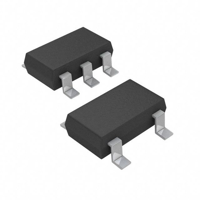
PACKAGES:
5-Pin SOT23W
(Suffix LH)
4-Pin SIP
(Suffix K)
Not to scale
VDD
Regulator
To All
Subcircuits
OUTPUTA
Z Hall
Low-Pass
Filter
Amp
Sample, Hold
& Averaging
Demultiplexer
X/Y Hall
Dynamic Offset
Cancellation &
Multiplexer
Current
Limit
OUTPUTB
Current
Limit
Functional Block Diagram
A1262-DS, Rev. 7
MCO-0000158
GND
November 18, 2020
�A1262
2D Dual-Channel Ultrasensitive Hall-Effect Latch
DESCRIPTION (continued)
On a single silicon chip, the A1262 includes: voltage regulator, reverse
battery protection, two Hall plates (one planar and one vertical), a
multiplexer, a small-signal amplifier, chopper stabilization, a Schmitt
trigger, and two short-circuit protected open-drain outputs that can
sink up to 20 mA continuously.
(E temperature range option) or –40°C to 150°C (L temperature
range option).
The A1262 is available in a 5-pin SOT23W surface-mount package
(LH) and a 4 pin SIP package (K). Each is offered in two options for
a variety of magnet to sensor orientations. The packages are RoHS
compliant and lead (Pb) free, with 100% matte-tin leadframe plating.
The A1262 is available in two temperature ranges: –40°C to 85°C
RoHS
COMPLIANT
SELECTION GUIDE
Part Number
Packing
Package
Temperature Range, TA (°C)
A1262ELHLT-T
7-in. reel, 3000 pieces/reel
5-pin SOT-23W surface mount
A1262ELHLX-T
13-in. reel, 10000 pieces/reel
5-pin SOT-23W surface mount
Description
–40 to 85
2 Outputs of Y and Z
A1262LK-Y-T
Bulk bag, 500 pieces/bag
4-pin SIP through-hole
A1262LLHLT-T
7-in. reel, 3000 pieces/reel
5-pin SOT-23W surface mount
A1262LLHLX-T
13-in. reel, 10000 pieces/reel
5-pin SOT-23W surface mount
A1262ELHLT-X-T
7-in. reel, 3000 pieces/reel
5-pin SOT-23W surface mount
A1262ELHLX-X-T
13-in. reel, 10000 pieces/reel
5-pin SOT-23W surface mount
A1262LK-X-T
Bulk bag, 500 pieces/bag
4-pin SIP through-hole
A1262LLHLT-X-T
7-in. reel, 3000 pieces/reel
5-pin SOT-23W surface mount
A1262LLHLX-X-T
13-in. reel, 10000 pieces/reel
5-pin SOT-23W surface mount
–40 to 150
–40 to 85
2 Outputs of X and Z
–40 to 150
Terminal List Table
Number
4
GND
3
OUTPUTB
VCC
2
OUTPUTA
1
Package K, 4-Pin SIP Pinout
4
GND
3
OUTPUTB
VDD
2
2
OUTPUTA
3
3
OUTPUTB
4
4
GND
Ground
–
5
GND
Ground
Connects power supply to chip
Output of Z magnetic field direction [1]
Default option: Output of Y magnetic field direction
With -X option: Output of X magnetic field direction
Z-axis recommended for use as the speed channel in a speed and direction application, due to better
repeatability.
ΔZ
ΔZ
OUTPUTA
2
Δ
X
Δ
X
1
GND
1
1
5
1
Y
Δ
1
Description
LH
Y
Δ
VDD
[1]
Symbol
K
Package LH, 5-Pin SOT23W Pinout
Allegro MicroSystems
955 Perimeter Road
Manchester, NH 03103-3353 U.S.A.
www.allegromicro.com
2
�A1262
2D Dual-Channel Ultrasensitive Hall-Effect Latch
ABSOLUTE MAXIMUM RATINGS
Characteristic
Symbol
Notes
Rating
Unit
26.5
V
Forward Supply Voltage
VDD
Reverse Supply Voltage
VRDD
–16
V
B
Unlimited
G
Magnetic Flux Density
Output Off Voltage
Output Sink Current
Maximum Junction Temperature
VOUT
26.5
V
IOUT(SINK)
Internally Limited
mA
165
°C
175
°C
–65 to 170
°C
TJ(MAX)
Storage Temperature
For 500 hours
Tstg
THERMAL CHARACTERISTICS: May require derating at maximum conditions; see application information
Characteristic
Symbol
Package Thermal Resistance
RθJA
Notes
Rating
Unit
Package K, single-sided PCB with copper limited to solder pads
177
°C/W
Package LH-5 4-layer board based on the JEDEC standard
124
°C/W
Power Dissipation, PD (mW)
* Additional thermal information available on the Allegro website.
1900
1800
1700
1600
1500
1400
1300
1200
1100
1000
900
800
700
600
500
400
300
200
100
0
4-L
ay
Sin
er
P
(R CB,
θJ
P
A=
12 ack
4ºC ag
/W e LH
)
-5
gle
-Sid
e
dP
(R
C
θJA =
177 B, Pa
ºC/
W) ckage
K
20
40
60
80
100
120
140
160
180
Temperature (°C)
Maximum Power Dissipation versus Ambient Temperature
Allegro MicroSystems
955 Perimeter Road
Manchester, NH 03103-3353 U.S.A.
www.allegromicro.com
3
�A1262
2D Dual-Channel Ultrasensitive Hall-Effect Latch
ELECTRICAL CHARACTERISTICS: Valid over full operating voltage and TA = –40°C to 85°C (Range E) or TA = –40°C to 150°C (Range L),
unless otherwise specified.
Characteristics
Symbol
Forward Supply Voltage
VDD
Output Leakage Current
IOUTOFF
Output On Voltage
VOUT(SAT)
Supply Current
IDD
Reverse-Battery Current
IRDD
Supply Zener Clamp Voltage
Output Current
VZ
Test Conditions
Min.
Typ. [1]
Max.
Unit
Operating, TJ < 165°C
4
–
24
V
B < BRP
–
–
10
µA
IOUT = 20 mA, B > BOP
–
180
500
mV
2
3
4.5
mA
VRDD = –16 V
–
–
–5
mA
ICC = 5 mA; TA = 25°C
28
34
–
V
–
–
20
mA
Output Short-Circuit Current Limit
IOUT(SINK)LIM
IOUT
TJ < TJ(max), VOUT = 12 V
30
–
60
mA
Output Sink Current, Peak
IOUT(SINK)PK
t < 3 seconds
–
–
110
mA
–
800
–
kHz
–
µs
Chopping Frequency
fC
Output Rise Time [2][3]
tr
RL = 820 Ω, CS = 20 pF
–
0.2
tf
RL = 820 Ω, CS = 20 pF
–
0.1
–
µs
Both channels, VDD > VDD(MIN)
–
32
48
µs
Output Fall Time
[2][3]
Power-On Time [2]
Power-On State
tON
POS
VDD > VDD(MIN), t< tON
Low
–
Typical data are at TA = 25°C and VDD = 4 V.
Power-on time, rise time, and fall time are guaranteed through device characterization.
[3] C = oscilloscope probe capacitance.
S
[1]
[2]
Allegro MicroSystems
955 Perimeter Road
Manchester, NH 03103-3353 U.S.A.
www.allegromicro.com
4
�A1262
2D Dual-Channel Ultrasensitive Hall-Effect Latch
MAGNETIC CHARACTERISTICS: Valid over full operating voltage and TA = –40°C to 85°C (Range E) or TA = –40°C to 150°C (Range L),
unless otherwise specified.
Characteristics
Operate Point
Symbol
[5]
BOP
Release Point [5]
BRP
Hysteresis
Min.
BOP – BRP
Typ.
Max.
Unit [4]
1
17
40
G
–40
–17
–1
G
15
34
68
G
Symmetry: Channel A, Channel B,
BOP(A) + BRP(A), BOP(B) + BRP(B)
BSYM(A),
BSYM(B)
–35
–
35
G
Operate Symmetry: BOP(A) – BOP(B)
BSYM(AB,OP)
–25
–
25
G
Release Symmetry: BRP(A) – BRP(B)
BSYM(AB,RP)
–25
–
25
G
[4] 1
BHYS
Test Conditions
G (gauss) = 0.1 mT (millitesla)
to all directions (X/Y and Z).
[5] Applicable
N
N
S
N
N
S
S
X
S
S
N
1
Y
Y
X
S
Z
Z
N
The A1262 output is turned on when presented with a south polarity magnetic field beyond BOP in the orientations illustrated above.
The X-axis field response is only applicable to the -X option; the Y-axis field response is only applicable to the default option. Note that
magnetic polarity between the LH and K X-axis options are opposite.
Allegro MicroSystems
955 Perimeter Road
Manchester, NH 03103-3353 U.S.A.
www.allegromicro.com
5
�A1262
2D Dual-Channel Ultrasensitive Hall-Effect Latch
CHARACTERISTIC DATA
Average Supply Current vs. Supply Voltage
8
8
7
7
6
4V
5
24 V
4
3
2
1
0
Supply Current, IDD (mA)
Supply Current, IDD (mA)
Average Supply Current vs. Ambient Temperature
-40°C
6
25°C
5
150°C
4
3
2
1
0
-60
-40
-20
0
20
40
60
80
100 120 140 160
2
6
10
Ambient Temperature, TA (°C)
VOUT(SAT)-B
0
20
40
60
80
100 120 140 160
Ambient Temperature, TA (°C)
Output Leakage Current, IOUTOFF (µA)
Output On Voltage, VOUT(SAT) (mV)
VOUT(SAT)-A
-60 -40 -20
Avg. OUTPUTA Operate Point vs. Ambient
Temperature
30
25
20
4V
24 V
5
26
0
10
8
IOUT(OFF)-A
6
IOUT(OFF)-B
4
2
0
-60
-40
-20
0
20
40
60
80
100 120 140 160
Ambient Temperature, TA (°C)
40
Operate Point, BOP (G)
Operate Point, BOP (G)
35
10
22
Avg. OUTPUTA Operate Point vs. Supply Voltage
40
15
18
Avg. Output Leakage Current vs. Ambient
Temperature
Avg. Output On Voltage vs. Ambient Temperature
500
450
400
350
300
250
200
150
100
50
0
14
Supply Voltage, VDD (V)
35
-40°C
30
25°C
25
150°C
20
15
10
5
0
-60
-40
-20
0
20
40
60
80
100 120 140 160
Ambient Temperature, TA (°C)
2
6
10
14
18
22
26
Supply Voltage, VDD (V)
Allegro MicroSystems
955 Perimeter Road
Manchester, NH 03103-3353 U.S.A.
www.allegromicro.com
6
�A1262
2D Dual-Channel Ultrasensitive Hall-Effect Latch
CHARACTERISTIC DATA (continued)
Avg. OUTPUTB Operate Point vs. Ambient
Temperature
Avg. OUTPUTB Operate Point vs. Supply Voltage
40
35
30
25
20
15
4V
10
24 V
5
Operate Point, BOP (G)
Operate Point, BOP (G)
40
0
-60
-40
-20
0
20
40
60
80
35
25°C
25
150°C
20
15
10
5
0
100 120 140 160
2
Ambient Temperature, TA (°C)
6
14
18
22
26
Avg. OUTPUTA Release Point vs. Supply Voltage
0
0
-5
-10
-15
-20
-25
4V
-30
24 V
-35
Release Point, BRP (G)
-5
-40
-10
-15
-20
-25
-40°C
-30
25°C
-35
150°C
-40
-60
-40
-20
0
20
40
60
80
100 120 140 160
2
6
Ambient Temperature, TA (°C)
10
14
18
22
26
Supply Voltage, VDD (V)
Avg. OUTPUTB Release Point vs. Supply Voltage
Avg. OUTPUTB Release Point vs. Ambient
Temperature
0
0
-5
-5
-10
-15
-20
-25
4V
-30
24 V
-35
Release Point, BRP (G)
Release Point, BRP (G)
10
Supply Voltage, VDD (V)
Avg. OUTPUTA Release Point vs. Ambient
Temperature
Release Point, BRP (G)
-40°C
30
-10
-15
-20
-25
-40°C
-30
25°C
-35
150°C
-40
-40
-60
-40
-20
0
20
40
60
80
100 120 140 160
Ambient Temperature, TA (°C)
2
6
10
14
18
22
26
Supply Voltage, VDD (V)
Allegro MicroSystems
955 Perimeter Road
Manchester, NH 03103-3353 U.S.A.
www.allegromicro.com
7
�A1262
2D Dual-Channel Ultrasensitive Hall-Effect Latch
CHARACTERISTIC DATA (continued)
Avg. OUTPUTA Hysteresis vs. Ambient
Temperature
Avg. OUTPUTA Hysteresis vs. Supply Voltage
70
60
4V
50
24 V
40
30
20
10
Hysteresis, BHYS (G)
Hysteresis, BHYS (G)
70
-40°C
60
25°C
50
150°C
40
30
20
10
-60
-40
-20
0
20
40
60
80
100 120 140 160
2
6
10
Ambient Temperature, TA (°C)
Avg. OUTPUTB Hysteresis vs. Ambient
Temperature
40
30
Hysteresis, BHYS (G)
Hysteresis, BHYS (G)
24 V
20
10
26
-40°C
60
25°C
50
150°C
40
30
20
10
-60
-40
-20
0
20
40
60
80
100 120 140 160
2
6
10
Ambient Temperature, TA (°C)
14
18
22
26
Supply Voltage, VDD (V)
Avg. BOP(A)+BRP(A) Symmetry vs. Ambient
Temperature
Avg. BOP(B)+BRP(B) Symmetry vs. Ambient
Temperature
15
10
4V
5
24 V
0
-5
-10
-15
Symmetry, BSYM(B) (G)
15
Symmetry, BSYM(A) (G)
22
70
4V
50
18
Avg. OUTPUTB Hysteresis vs. Supply Voltage
70
60
14
Supply Voltage, VDD (V)
10
4V
5
24 V
0
-5
-10
-15
-60
-40
-20
0
20
40
60
80
100 120 140 160
Ambient Temperature, TA (°C)
-60
-40
-20
0
20
40
60
80
100 120 140 160
Ambient Temperature, TA (°C)
Allegro MicroSystems
955 Perimeter Road
Manchester, NH 03103-3353 U.S.A.
www.allegromicro.com
8
�A1262
2D Dual-Channel Ultrasensitive Hall-Effect Latch
CHARACTERISTIC DATA (continued)
Avg. BOP(A)–BOP(B) Symmetry vs. Ambient
Temperature
Avg. BRP(A)–BRP(B) Symmetry vs. Ambient
Temperature
15
10
4V
5
24 V
0
-5
-10
-15
Symmetry, BSYM(AB,RP) (G)
Symmetry, BSYM(AB,OP) (G)
15
10
4V
5
24 V
0
-5
-10
-15
-60
-40
-20
0
20
40
60
80
100 120 140 160
Ambient Temperature, TA (°C)
-60
-40
-20
0
20
40
60
80
100 120 140 160
Ambient Temperature, TA (°C)
Allegro MicroSystems
955 Perimeter Road
Manchester, NH 03103-3353 U.S.A.
www.allegromicro.com
9
�A1262
2D Dual-Channel Ultrasensitive Hall-Effect Latch
FUNCTIONAL DESCRIPTION
Operation
V+
This built-in hysteresis allows clean switching of the output even
in the presence of external mechanical vibration and electrical
noise. The device will power-on in the low output state, even
when powering-on in the hysteresis region, between BOP and BRP.
Unlike dual-planar Hall-effect sensors, which have two planar
Hall-effect sensing elements spaced apart across the width of the
package, both the vertical and planar sensing elements on the
A1262 are located in essentially the same location on the IC.
dual
planar
Switch to High
VOUTPUT
B-
BRP
VOUT(ON)
0
BOP
Removal of the magnetic field will leave the device output
latched on if the last crossed switch point is BOP, or latched off if
the last crossed switch point is BRP.
VOUT(OFF)
Switch to Low
The outputs of the A1262 switch low (turn on) when the corresponding Hall element is presented with a perpendicular south
magnetic field of sufficient strength. OUTPUTA switches low if
the Z-axis direction exceeds the operate point (BOP), and OUTPUTB switches low if the Y-axis direction (A1262 with default
option) or X-axis direction (A1262 with -X option) exceeds BOP.
After turn-on, the output voltage is VOUT(SAT). The device outputs
switch high (turn off) when the strength of a perpendicular north
magnetic field exceeds the release point (BRP). The difference in
the magnetic operate and release points is the hysteresis (BHYS)
of the device. See Figure 1.
B+
BHYS
Figure 1: Switching Behavior of Latches
On the horizontal axis, the B+ direction indicates increasing
south polarity magnetic field strength, and the B– direction
indicates decreasing south polarity field strength (including
the case of increasing north polarity
With dual-planar Hall sensors, the ring magnet must be properly
designed and optimized for the physical Hall spacing (distance)
in order to have the outputs of the two latches to be in quadrature, or 90 degrees out of phase. With the A1262, which uses one
planar and one vertical Hall-effect sensing element, no target
optimization is required. When the face of the IC is facing the
ring magnet, the planar Hall senses the magnet poles and the
vertical Hall senses the transition between poles, therefore the
A1262
Dual-Planar
Sensor
A1262
Figure 2: Ring magnet optimized for a dual-planar Hall-effect sensor resulting in output
quadrature also results in quadrature for the A1262.
Allegro MicroSystems
955 Perimeter Road
Manchester, NH 03103-3353 U.S.A.
www.allegromicro.com
10
�A1262
2D Dual-Channel Ultrasensitive Hall-Effect Latch
two channels will inherently be in quadrature, irrespective of the
ring-magnet pole spacing.
Figure 2 above shows a ring magnet optimized for the E1-to-E2
spacing of a dual-planar sensor, resulting in quadrature, or 90
degrees phase separation between channels. This same target
also results in quadrature for the 2D sensing A1262. However
when a different ring magnet is used which is not optimized for
dual
planar
the E1-to-E2 spacing, the dual-planar sensor exhibits diminished
phase separation, making signal processing the outputs into speed
and direction less robust. Using a different ring-magnet geometry has no effect on the A1262, and the two channels remain in
quadrature (see Figure 3 below).
The relationship of the various signals and the typical system timing is shown in Figure 4.
A1262
Dual-Planar
Sensor
A1262
Figure 3: Ring magnet not optimized for a dual-planar Hall-effect sensor resulting in significantly reduced output phase separation, however still results in quadrature for the A1262.
Figure 4: Typical System Timing
The Planar (P) and Vertical (V) signals represent the magnetic input signal, which is converted to the device outputs,
OUTPUTA and OUTPUTB, respectively. While the A1262 does not process the signals into Speed and Direction, these
could be determined by the user based on the individual output signals.
Allegro MicroSystems
955 Perimeter Road
Manchester, NH 03103-3353 U.S.A.
www.allegromicro.com
11
�A1262
2D Dual-Channel Ultrasensitive Hall-Effect Latch
Output Response to a
Speed and Direction Part
2
Clockwise Rotation
1
Bx
Bz
Counterclockwise Rotation
Bz
Time
(s)
Bx
Vertical
Time
(s)
Planar
3
Bx
A1262
4
Time
(s)
Figure 5: Typical System Timing
The two active Hall signals represent the magnetic input signal,
which is converted to the device outputs, OUTPUTA and
OUTPUTB.
Allegro MicroSystems
955 Perimeter Road
Manchester, NH 03103-3353 U.S.A.
www.allegromicro.com
12
�A1262
2D Dual-Channel Ultrasensitive Hall-Effect Latch
Sampling
Cycle
Channel A
Channel B
Channel A
Channel B
Channel A
Channel B
Channel A
Channel B
Channel A
Channel B
t
BOP(A)
0
BRP(A)
t
BOP(B)
0
BRP(B)
t
Signal OUTPUTA
0
t
Signal OUTPUTB
0
Sampling
Cycle
Channel B
t
Channel A
Channel B
Sampling
Cycle
Channel A
Channel B
Channel A
Channel B
Channel A
t
t
BOP(A)
BOP(A)
0
BRP(A)
Signal
OUTPUTA
0
t
t
0
BRP(A)
t
Signal
OUTPUTA
0
Figure 6: Output signal updating with respect to the channel sampling
The two active channels are multiplexed with a typical 16 µs
sampling period per channel. If the magnetic signal crosses the
respective BOP or BRP of a particular channel, that channel’s
output will not be updated until the end of its sampling period.
If the signal crosses the thresholds while the alternate channel is
sampling, the update will occur at the end of the next sampling
period (as long as the signal does not cross back over the
t
thresholds). This is illustrated in Figure 6. The sampling error
introduced by the multiplexing increases with magnetic input
frequency, which can affect the output duty cycle and phase
separation between outputs. Contact your Allegro representative
for more information regarding suitability to high frequency
applications.
Allegro MicroSystems
955 Perimeter Road
Manchester, NH 03103-3353 U.S.A.
www.allegromicro.com
13
�A1262
2D Dual-Channel Ultrasensitive Hall-Effect Latch
A1262 Sensor and Relationship to Target
The A1262 is available in two sensing options: with Z-axis planar
Hall and the Y-axis vertical Hall active (default option), or with
the Z-axis planar Hall and the X-axis vertical Hall active (-X
option). This offers incredible flexibility for positioning the IC
within various applications.
Figure 7a: LH (-Y option)
The Z-Y option supports the traditional configuration with the
face of the package facing the ring magnet (Figure 7a or 7c), with
the axis of rotation going cross the leads, or opposide the leaded
side(s) of the package facing the ring magnet (Figure 7b or 7d).
Figure 7b: LH (-Y option)
Figure 7c: K (-Y option)
Figure 7d: K (-Y option)
Allegro MicroSystems
955 Perimeter Road
Manchester, NH 03103-3353 U.S.A.
www.allegromicro.com
14
�A1262
2D Dual-Channel Ultrasensitive Hall-Effect Latch
The Z-X option supports having the IC positioned with the face
of the package facing the ring magnet, and the axis of rotation
(Figure 8a or 8c) lengthwise along the package body, or with
either of the non-leaded sides of the package facing the ring mag-
net (Figure 8b or 8d). This latter configuration has the advantage
of being able to be mounted extremely close to the ring magnet,
since there are no leads or solder pads to accommodate for in that
dimension.
Figure 8a: LH (-X option)
Figure 8b: LH (-X option)
Figure 8c: K (-X option)
Figure 8d: K (-X option)
Allegro MicroSystems
955 Perimeter Road
Manchester, NH 03103-3353 U.S.A.
www.allegromicro.com
15
�A1262
2D Dual-Channel Ultrasensitive Hall-Effect Latch
Power-On Sequence and Timing
Applications
The states of OUTPUTA and OUTPUT B are only valid when the
supply voltage is within the specified operating range (VDD(MIN)
≤ VDD ≤ VDD(MAX)) and the power-on time has elapsed (t > tON).
Refer to Figure 9: Power-On Sequence and Timing for an illustration of the power-on sequence.
It is strongly recommended that an external capacitor be connected (in close proximity to the Hall sensor) between the supply
and ground of the device to reduce both external noise and noise
generated by the chopper stabilization technique. As shown in
Figure 10, a 0.1 µF capacitor is typical.
V
VS
VOUT(OFF)
Planar
(Z)
Output Undefined for
VDD < VDD(MIN)
VOUT(ON)
0
POS
V
Output Responds According
to Magnetic Field Input
B > BOP or B < BRP
t > tON(MAX)
time
Output Undefined for
VDD < VDD(MIN)
VOUT(ON)
0
POS
Output Responds According
to Magnetic Field Input
B > BOP or B < BRP
t > tON(MAX)
time
V
RLOAD
OUTPUTA
OUTPUTB
Sensor
Outputs
GND
Figure 10: Typical Application Circuit
Extensive applications information on magnets and Hall-effect
sensors is available in:
VDD(MIN)
• Hall-Effect IC Applications Guide, AN27701,
VDD
0
CBYP
0.1 µF
RLOAD
GND
VOUT(OFF)
Vertical
(X/Y)
VDD
A1262
t ON
time
Figure 9: Power-On Sequence and Timing
Once the supply voltage is within the operational range, the
outputs will be in the low state (power-on state), irrespective of
the magnetic field. The outputs will remain low until the sensor
is fully powered on (t > tON), at which point, both outputs will
respond to the corresponding magnetic field presented to the sensor (the vertical Hall channel typically responds before the planar
Hall channel).
• Hall-Effect Devices: Guidelines for Designing Subassemblies
Using Hall-Effect Devices, AN27703.1
• Soldering Methods for Allegro’s Products – SMD and
Through-Hole, AN26009
• Air-Gap-Independent Speed and Direction Sensing Using the
Allegro A1262, AN296124
• Improved Speed and Direction Sensing Using Vertical Hall
Technology, AN296130
All are provided on the Allegro website:
www.allegromicro.com
Allegro MicroSystems
955 Perimeter Road
Manchester, NH 03103-3353 U.S.A.
www.allegromicro.com
16
�A1262
2D Dual-Channel Ultrasensitive Hall-Effect Latch
Chopper Stabilization Technique
When using Hall-effect technology, a limiting factor for switchpoint accuracy is the small signal voltage developed across the
Hall element. This voltage is disproportionally small relative to
the offset that can be produced at the output of the Hall sensor.
This makes it difficult to process the signal while maintaining an
accurate, reliable output over the specified operating temperature
and voltage ranges.
Chopper stabilization is a proven approach used to minimize
Hall offset on the chip. The Allegro technique, namely Dynamic
Quadrature Offset Cancellation, removes key sources of output
drift induced by thermal and mechanical stresses. This technique
is based on a signal modulation-demodulation process. The
undesired offset signal is separated from the magnetic fieldinduced signal in the frequency domain, through modulation.
The subsequent demodulation acts as a modulation process for
the offset, causing the magnetic field induced signal to recover
its original spectrum at baseband, while the DC offset becomes a
high-frequency signal. The magnetic sourced signal then can pass
through a low-pass filter, while the modulated DC offset is suppressed. This configuration is illustrated in Figure 11.
The chopper stabilization technique uses a 400 kHz highfrequency clock. For demodulation process, a sample, hold, and
averaging technique is used, where the sampling is performed
at twice the chopper frequency (800 kHz). This high-frequency
operation allows a greater sampling rate, which results in higher
accuracy and faster signal-processing capability. This approach
desensitizes the chip to the effects of thermal and mechanical stresses, and produces devices that have extremely stable
quiescent Hall output voltages and precise recoverability after
temperature cycling. This technique is made possible through the
use of a BiCMOS process, which allows the use of low-offset,
low-noise amplifiers in combination with high-density logic and
sample-and-hold circuits.
Multiplexer
VDD
Low-Pass
Filter
Sample, Hold &
Averaging
Amp.
Figure 11: Model of Chopper Stabilization Technique
Allegro MicroSystems
955 Perimeter Road
Manchester, NH 03103-3353 U.S.A.
www.allegromicro.com
17
�A1262
2D Dual-Channel Ultrasensitive Hall-Effect Latch
POWER DERATING
The device must be operated below the maximum junction
temperature of the device, TJ(max). Under certain combinations of
peak conditions, reliable operation may require derating supplied
power or improving the heat dissipation properties of the application. This section presents a procedure for correlating factors
affecting operating TJ. (Thermal data is also available on the
Allegro MicroSystems website.)
The Package Thermal Resistance (RθJA) is a figure of merit summarizing the ability of the application and the device to dissipate
heat from the junction (die), through all paths to the ambient air.
Its primary component is the Effective Thermal Conductivity (K)
of the printed circuit board, including adjacent devices and traces.
Radiation from the die through the device case (RθJC) is relatively
small component of RθJA. Ambient air temperature (TA) and air
motion are significant external factors, damped by overmolding.
The effect of varying power levels (Power Dissipation, PD), can
be estimated. The following formulas represent the fundamental
relationships used to estimate TJ at PD.
A worst-case estimate (PD(max)) represents the maximum allowable power level (VDD(max), IDD(max)), without exceeding TJ(max),
at a selected RθJA and TA.
Example: Reliability for VDD at TA = 150°C, package LH5, using
low-K PCB.
Observe the worst-case ratings for the device, specifically:
RθJA = 124°C/W, TJ(max) = 165°C, VDD(max) = 24 V, and
IDD(max) = 7.5 mA.
Calculate the maximum allowable power level (PD(max)). First,
invert equation 3:
∆Tmax = TJ(max) – TA = 165°C – 150°C = 15°C
This provides the allowable increase to TJ resulting from internal
power dissipation. Then, invert equation 2:
PD(max) = ∆Tmax ÷ RθJA = 15°C ÷ 124°C/W = 121 mW
Finally, invert equation 1 with respect to voltage:
PD = VIN × IIN
(1)
VDD(est) = PD(max) ÷ IDD(max)
∆T = PD × RθJA (2)
VDD(est) = 121 mW ÷ 7.5 mA
TJ = TA + ∆T
(3)
For example, given common conditions such as: TA = 25°C,
VDD = 12 V, IDD = 3 mA, and RθJA = 124°C/W for the LH5 package, then:
PD = VDD × IDD = 12 V × 3.0 mA = 36.0 mW
∆T = PD × RθJA = 36.0 mW × 124°C/W = 4.5°C
VDD(est) = 16.1 V
The result indicates that, at TA, the application and device can
dissipate adequate amounts of heat at voltages ≤ VDD(est).
Compare VDD(est) to VDD(max). If VDD(est) ≤ VDD(max), then reliable operation between VDD(est) and VDD(max) requires enhanced
RθJA. If VDD(est) ≥ VDD(max), then operation between VDD(est) and
VDD(max) is reliable under these conditions.
TJ = TA + ∆T = 25°C + 4.5°C = 29.5°C
Allegro MicroSystems
955 Perimeter Road
Manchester, NH 03103-3353 U.S.A.
www.allegromicro.com
18
�A1262
2D Dual-Channel Ultrasensitive Hall-Effect Latch
PACKAGE OUTLINE DRAWINGS
E
+0.08
5.21 –0.05
E1
45°
E
B
E3
E2
2.60
0.11
1.32
+0.08
3.43 –0.05
E
E1
E
E2
D
E
0.17
E2 E
E3
1.55 ±0.05
2.16
MAX
E
E
Branded
Face
E1
E
E3
2
3
1
D Standard Branding Reference View
0.84 REF
N = Device part number
Y = Last two digits of year of manufacture
W = Week of manufacture
For Reference Only; not for tooling use (reference DWG-9010)
Dimensions in millimeters
Dimensions exclusive of mold flash, gate burrs, and dambar protrusions
Exact case and lead configuration at supplier discretion within limits shown
4
14.73 ±0.51
+0.06
0.38 –0.03
+0.07
0.41 –0.05
YYWW
45°
A
1
NNNN
Mold Ejector
Pin Indent
A
Dambar removal protrusion (8×)
B
Gate and tie bar burr area
C
Branding scale and appearance at supplier discretion
D Active Area Depth, 0.42 mm
E Hall Elements (E1, E2, and E3), not to scale;
E2 and E3 are active in the A1262LK-T;
E1 and E3 are active in the A1262LK-X-T
1.27 NOM
Figure 12: Package K, 4-Pin SIP
Allegro MicroSystems
955 Perimeter Road
Manchester, NH 03103-3353 U.S.A.
www.allegromicro.com
19
�A1262
2D Dual-Channel Ultrasensitive Hall-Effect Latch
For Reference Only – Not for Tooling Use
(Reference DWG-0000628)
Dimensions in millimeters – NOT TO SCALE
Dimensions exclusive of mold flash, gate burrs, and dambar protrusions
Exact case and lead configuration at supplier discretion within limits shown
AY
+0.12
2.98
–0.08
D
0.11
REF
2.90
4° ±4°
AZ
AX
5
+0.020
0.180
–0.053
D1 D
D1 D
+0.10
–0.20
1.91
+0.19
–0.06
D3 D
D D2
1
2
0.17
D REF
D2 D
0.25 MIN
D D3
0.55
REF
D3 D
0.25 BSC
Branded Face
SEATING PLANE
GAUGE PLANE
8× 10° ±5°
REF
1.00 ±0.13
D D2
+0.10
0.05
–0.05
0.40 ±0.10
0.95
BSC
D1 D
0.20 MIN
NNN
2.40
C
Standard Branding Reference View
AX Active Area Distance, X Axis, 1.49 nominally. AX is measured from the edge of the
package to the sensitive element; therefore, the tolerances are reflected in the body
length dimension.
1.00
0.70
AY Active Area Distance, Y Axis, 0.955 nominally. AY is measured from the edge of the
package to the sensitive element; therefore, the tolerances are reflected in the body
width dimension.
0.95
B PCB Reference Layout View
AZ Active Area Depth, Z Axis, 0.28 ±0.04
B
Reference land pattern layout; all pads a minimum of 0.20 mm from all adjacent pads;
adjust as necessary to meet application process requirements and PCB layout tolerances
C
Branding Scale and appearance at supplier discretion
D
Hall Elements (D1, D2, and D3), not to scale; D2 and D3 are active in the A1262LLH-T;
D1 and D3 are active in the A1262LLH-X-T
Figure 13: Package LH, 5-Pin SOT23-W
Allegro MicroSystems
955 Perimeter Road
Manchester, NH 03103-3353 U.S.A.
www.allegromicro.com
20
�A1262
2D Dual-Channel Ultrasensitive Hall-Effect Latch
Revision History
Number
Date
Description
–
September 21, 2015
Initial release
1
February 10, 2016
Added E temperature range option and magnetic switch point symmetry specifications
2
February 10, 2017
Updated Features and Benefits (page 1), Description (pages 1-2), Absolute Maximum Ratings table
(page 3), Electrical Characteristics table (page 4), Figure 5 (page 12), Figure 6 (page 13), Figure
7 and 8 labels (pages 14-15), Chopper Stabilization section (page 17); added Typical Applications;
added K package option; expanded Functional Description section.
3
May 19, 2017
Corrected Pinout Diagrams (page 2).
4
July 31, 2017
Updated Selection Guide table (page 2).
5
August 8, 2018
Minor editorial updates.
6
August 22, 2019
Minor editorial updates.
7
November 18, 2020
Update Package Outline Drawing active area distances (page 20).
Copyright 2020, Allegro MicroSystems.
Allegro MicroSystems reserves the right to make, from time to time, such departures from the detail specifications as may be required to permit
improvements in the performance, reliability, or manufacturability of its products. Before placing an order, the user is cautioned to verify that the
information being relied upon is current.
Allegro’s products are not to be used in any devices or systems, including but not limited to life support devices or systems, in which a failure of
Allegro’s product can reasonably be expected to cause bodily harm.
The information included herein is believed to be accurate and reliable. However, Allegro MicroSystems assumes no responsibility for its use; nor
for any infringement of patents or other rights of third parties which may result from its use.
Copies of this document are considered uncontrolled documents.
For the latest version of this document, visit our website:
www.allegromicro.com
Allegro MicroSystems
955 Perimeter Road
Manchester, NH 03103-3353 U.S.A.
www.allegromicro.com
21
�