A1377
Highly Programmable Linear Hall-Effect Sensor IC
DESCRIPTION
FEATURES AND BENEFITS
• On-board diagnostics
□□ Broken ground detection
□□ VCC undervoltage detection
□□ VCC overvoltage detection
• Customer-programmable offset, sensitivity, polarity, and
output clamps
• Integrated power supply and output bypass capacitors
• Customer and factory access code for enhanced
reliability
□□ Factory code required for write access to TC trim and
other factory registers
□□ Customer code required for write access to customer
registers
The Allegro™ A1377 programmable linear Hall-effect sensor
IC is designed for applications that require high accuracy
and high resolution without compromising bandwidth. The
A1377 employs segmented, linearly interpolated temperature
compensation technology. This improvement greatly reduces
the total error of the device across the whole temperature
range. As a result, the device is ideally suited for sensing in
numerous automotive applications, such as linear and rotary
position sensors in actuators and valves.
Available in a through-hole, small form factor, single in-line
package (SIP), the A1377 Hall-effect sensor IC has a broad
range of sensitivity and offset operating bandwidth. The
accuracy and flexibility of this device is enhanced with user
programmability, via the VCC and output pins, which allows
the device to be optimized in the application.
Continued on the next page…
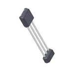
PACKAGE: 3-pin SIP (suffix UC)
This ratiometric Hall-effect sensor IC provides a voltage output
that is proportional to the applied magnetic field. The quiescent
voltage output (QVO) is user-adjustable from approximately
5% to 95% of the supply voltage. The device sensitivity is
adjustable within the range of 1 to 14 mV/G.
The features of this linear device make it ideal for use in
automotive and industrial applications requiring high accuracy,
and apply across an extended temperature range, from –40°C
to 150°C.
Not to scale
Continued on the next page…
A1377
IC
VCC
(Programming)
100 nF
Undervoltage
and Overvoltage
Detection
Regulator
Pulse
Generator
Level
Detector
EEPROM
Broken
Ground
Detection
To all
subcircuits
Temperature
Sensor
Dynamic Offset
Cncellation
Sensitivity
Control
Control Logic
Active
Temperature
Compensation
Offset
Control
Signal Recovery
PushPull
Address
Decoding
Output
Clamps
Transmit and
Receive Control
VOUT
(Programming)
100 nF
GND
Functional Block Diagram
A1377-DS, Rev. 2
MCO-0000607
February 22, 2019
�A1377
Highly Programmable Linear Hall-Effect Sensor IC
FEATURES AND BENEFITS (continued)
• Temperature-stable quiescent voltage output and sensitivity:
sensitivity temperature coefficient (TC) and QVO temperature
coefficient programmed at Allegro for improved accuracy
• Optional output voltage clamps provide short-circuit
diagnostic capabilities
• Wide ambient temperature range: –40°C to 150°C
• Enhanced EMC performance for stringent automotive
applications
DESCRIPTION (continued)
Each BiCMOS monolithic circuit integrates a Hall element,
temperature-compensating circuitry to reduce the intrinsic sensitivity
drift of the Hall element, a small-signal high-gain amplifier, a
clamped low-impedance output stage and a proprietary dynamic
offset cancellation technique.
The A1377 sensor is provided in a 3-pin single in-line package (UC
suffix) with bypass capacitors integrated into the package. It is lead
(PB) free, with 100% matte-tin leadframe plating.
SELECTION GUIDE
Part Number
Packing*
A1377LUCTN–TC[N]–T
4000 pieces per 13-inch reel
*Contact Allegro™ for additional packing options.
Configuration Option
A1377LUCTN - TCN - T
Leadframe plating – T : 100% matte tin
Temperature Compensation (%/°C)
TC1: 0.12 (Default; for NdFeB)
TC3: 0.035 (For SmCo)
Allegro Identifier and Device Type – A1377
Operating Temperature Range, TA – L: –40°C to 150°C
Package Designator – UC
Instructions (Packing) – TN: Tape and reel, 4000 pieces per 13-inch reel
Specifications
Pinout Diagram and Terminal List
Operating Characteristics
Characteristic Definitions
Functional Description
Diagnostic Conditions
Undervoltage Detection
Overvoltage Detection
Broken Ground Detection
EEPROM Diagnostics
EEPROM Margin Checking
3
3
4
8
12
12
12
12
12
12
12
Table of Contents
Application Information
Programming Guidelines
Serial Communication
Memory Address Map
Programmable Parameter Reference
Package Outline Drawing
14
15
15
19
21
24
Allegro MicroSystems, LLC
955 Perimeter Road
Manchester, NH 03103-3353 U.S.A.
www.allegromicro.com
2
�A1377
Highly Programmable Linear Hall-Effect Sensor IC
SPECIFICATIONS
ABSOLUTE MAXIMUM RATINGS
Rating
Unit
Forward Supply Voltage
Characteristic
Symbol
VCC
Notes
16
V
Reverse Supply Voltage
VRCC
–16
V
Forward Output Voltage
VOUT
VOUT < VCC + 2
16
V
Reverse Output Voltage
VROUT
TJ(max) not exceeded
–5
V
Output Source Current
IOUT(SOURCE)
VOUT to GND
10
mA
IOUT(SINK)
VCC to VOUT
–10
mA
At absolute maximum conditions, the device sinks not more
than 50 mA
–50
mA
–40 to 150
ºC
Output Sink Current
Reverse Supply Current
IRCC
Operating Ambient Temperature
TA
Maximum Junction Temperature
TJ(max)
165
ºC
Tstg
–65 to 170
ºC
Storage Temperature
L temperature range
THERMAL CHARACTERISTICS: May require derating at maximum conditions; see application information
Characteristic
Symbol
Package Thermal Resistance
RθJA
Test Conditions*
Estimated, on single-layer PCB with copper limited to solder
pads
Value
Unit
201
ºC/W
*Additional thermal information available on the Allegro website.
1
2
3
VCC
GND
VOUT
Terminal List Table
Number
Name
Function
1
VCC
Device power supply, also used for
programming
2
GND
Device ground
3
VOUT
Output signal, also used for programming
UC Package Pinout Diagram
Allegro MicroSystems, LLC
955 Perimeter Road
Manchester, NH 03103-3353 U.S.A.
www.allegromicro.com
3
�A1377
Highly Programmable Linear Hall-Effect Sensor IC
OPERATING CHARACTERISTICS: Valid across full TA range, CBYPASS = 0.1 µF (internal), VCC = 5 V, unless otherwise specified
Characteristic
Symbol
Test Conditions
Min.
Typ.
Max.
Unit 1
4.5
5
5.5
V
ELECTRICAL CHARACTERISTICS
Supply Voltage
VCC
Supply Current
ICC
No load on VOUT
Reverse Supply Current
IRCC
VCC = –15 V, TA = 25°C
Power-On Time 2
tPO
Delay to Clamp 2
tCLP
Internal Bandwidth
BWi
–
7.5
10
mA
–10
–
–
mA
TA = 25°C, CLOAD(PROBE) = 10 pF
–
400
2000
µs
TA = 25°C, CLI = 100 nF
–
30
–
µs
Large signal –3 dB
–
2.5
–
kHz
fC
TA = 25°C
–
125
–
kHz
VN
TA = 25°C, CBYPASS = open, Sens = 2.5 mV/G,
no load on VOUT
–
2.1
6
mVRMS
Input-Referred RMS Noise Density 11
VNRMS
TA = 25°C, CBYPASS = open, no load on VOUT,
magnetic input signal frequency
很抱歉,暂时无法提供与“A1377LUCTN-TC3-T”相匹配的价格&库存,您可以联系我们找货
免费人工找货