A1688
Two-Wire, True Zero-Speed, High Accuracy Sensor IC
Not for New Design
These parts are in production but have been determined to be NOT FOR
NEW DESIGN. This classification indicates that sale of this device is
currently restricted to existing customer applications. The device should
not be purchased for new design applications because obsolescence in
the near future is probable. Samples are no longer available.
Date of status change: October 1, 2022
Recommended Substitutions:
For existing customer transition, and for new customers or new applications, refer to the A19200LUBATN-L, A19200LUBATN-H, or
A19250LUBATN.
NOTE: For detailed information on purchasing options, contact your
local Allegro field applications engineer or sales representative.
Allegro MicroSystems reserves the right to make, from time to time, revisions to the anticipated product life cycle plan for a
product to accommodate changes in production capabilities, alternative product availabilities, or market demand. The information included herein is believed to be accurate and reliable. However, Allegro MicroSystems assumes no responsibility for
its use; nor for any infringements of patents or other rights of third parties which may result from its use.
�A1688
Two-Wire, True Zero-Speed, High Accuracy Sensor IC
FEATURES AND BENEFITS
• Integrated capacitor reduces need for external EMI
protection components
• Wide leads facilitate ease of assembly
• True zero-speed operation
• Automatic Gain Control (AGC) for air gap independent
switch points
• Automatic Offset Adjustment (AOA) for signal
processing optimization
• Large operating air gap range
• Internal current regulator for two-wire operation
• Undervoltage lockout
• Single chip sensing IC for high reliability
• On-chip voltage regulator with wide operating voltage
range and stability in the presence of a variety of
complex load impedances
• Fully synchronous digital logic with Scan and IDDQ
testing
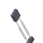
PACKAGE: 2-pin SIP (suffix UB)
DESCRIPTION
The A1688 is a Hall-effect-based integrated circuit (IC) that
provides a user-friendly solution for true zero-speed digital
ring magnet and gear tooth sensing in two-wire applications.
The A1688 is offered in the UB package, which integrates
the IC and a high temperature ceramic capacitor in a single
overmolded SIP package. The integrated capacitor provides
enhanced EMC performance with reduced external components.
The integrated circuit incorporates a dual-element Hall-effect
circuit and signal processing that switches in response to
differential magnetic signals created by magnetic encoders, or,
when properly back-biased with a magnet, from ferromagnetic
targets. The device contains a sophisticated digital circuit that
reduces magnet and system offsets, calibrates the gain for air
gap independent switch points, and provides true zero-speed
operation.
Signal optimization occurs at power-up through the combination
of offset and gain-adjust and is maintained throughout operation
with the use of a running-mode calibration scheme. Runningmode calibration provides immunity from environmental effects
such as micro-oscillations of the sensed target or sudden air
gap changes.
The regulated current output is configured for two-wire interface
circuitry and is ideally suited for obtaining speed information in
wheel speed applications. The Hall element spacing is optimized
for high resolution, small diameter targets. The package is lead
(Pb) free, with 100% matte-tin leadframe plating.
Not to scale
VCC
Internal Regulator
Amp
Offset
Adjust
AGC
Analog to
Digital
Converter
Digital
Controller
Output
Control
GND
Chopper
Stabilization
Functional Block Diagram
A1688-DS, Rev. 10
MCO-0000633
October 1, 2022
�A1688
Two-Wire, True Zero-Speed, High Accuracy Sensor IC
SPECIFICATIONS
SELECTION GUIDE
Part Number
Packing*
Power-On State
A1688LUBTN–L–T
4000 pieces per 13-in. reel
ICC(LOW)
A1688LUBTN–H–T
4000 pieces per 13-in. reel
ICC(HIGH)
*Contact Allegro™ for additional packing options.
ABSOLUTE MAXIMUM RATINGS
Characteristic
Symbol
Notes
Rating
Unit
Supply Voltage
VCC
28
V
Reverse Supply Voltage
VRCC
–18
V
Operating Ambient Temperature
TA
–40 to 150
ºC
Maximum Junction Temperature
TJ(max)
165
ºC
Tstg
–65 to 170
ºC
Value
(Typ.)
Unit
2200
pF
Storage Temperature
L temperature range
Internal Discrete Capacitor Ratings
Characteristic
Symbol
Nominal Capacitance
CSUPPLY
Test Conditions*
Connected between VCC and GND
Terminal List Table
1
2
Name
Number
Function
VCC
1
Supply Voltage
GND
2
Ground
UB Package, 2-Pin SIP Pinout Diagram
Allegro MicroSystems
955 Perimeter Road
Manchester, NH 03103-3353 U.S.A.
www.allegromicro.com
2
�A1688
Two-Wire, True Zero-Speed, High Accuracy Sensor IC
OPERATING CHARACTERISTICS: Valid throughout full operating and temperature ranges; unless otherwise specified
Characteristic
Symbol
Test Conditions
Min.
Typ.1
Max.
Unit
Operating, TJ < TJ(max)
4
–
24
V
VCC transitioning from 0 → 5 V or 5 → 0 V
–
3.6
3.95
V
VCC = VRCC(max)
–
–
–10
mA
ELECTRICAL CHARACTERISTICS
Supply Voltage2
Undervoltage Lockout
Reverse Supply Current3
VCC
VCC(UV)
IRCC
Supply Zener Clamp Voltage
VZSUPPLY
ICC = ICC(max) + 3 mA, TA = 25ºC
28
–
–
V
Supply Zener Current
IZSUPPLY
TA = 25°C, VCC = 28 V
–
–
19
mA
-H variant
–
ICC(HIGH)
–
–
OUTPUT
Power-On State
Supply Current
POS
–
ICC(LOW)
–
–
ICC(LOW)
-L variant
Low-current state
5.9
–
8.4
mA
ICC(HIGH)
High-current state
12
–
16
mA
ICC(HIGH) /
ICC(LOW)
Measured as ratio of high current to low current
(isothermal)
1.9
–
–
–
Output Rise Time
tr
Corresponds to measured output slew rate with
CSUPPLY; RLOAD = 100 Ω
0
–
1.5
μs
Output Fall Time
tf
Corresponds to measured output slew rate with
CSUPPLY; RLOAD = 100 Ω
0
–
1.5
μs
Supply Current Ratio
OPERATING CHARACTERISTICS
Operate Point
BOP
% of peak-to-peak IC-processed magnetic
signal
–
60
–
%
Release Point
BRP
% of peak-to-peak IC-processed magnetic
signal
–
40
–
%
Operating Frequency
fFWD
0
–
5
kHz
Continued on the next page…
VCC
1
VCC
A1688
GND
4
RLOAD
100 Ω
CLOAD
Figure 1: Typical Application Circuit
Allegro MicroSystems
955 Perimeter Road
Manchester, NH 03103-3353 U.S.A.
www.allegromicro.com
3
�A1688
Two-Wire, True Zero-Speed, High Accuracy Sensor IC
OPERATING CHARACTERISTICS (continued): Valid throughout full operating and temperature ranges; unless otherwise
specified
Characteristic
Symbol
Test Conditions
Min.
Typ.1
Max.
Unit
20
–
1200
G
–300
–
300
G
–
+0.2
–
%/°C
OPERATING CHARACTERISTICS (continued)
Input Signal
BSIG
Allowable User-Induced Differential
Offset
BSIGEXT
Sensitivity Temperature Coefficient4
TC
Differential signal, measured peak-to-peak
External differential signal bias (DC), operating
within specification
Total Pitch Deviation
For constant BSIG, sine wave
–
–
±2
%
Maximum Sudden Signal Amplitude
Change
BSEQ(n+1)
/ BSEQ(n)
No missed output edge. Instantaneous
symmetric magnetic signal amplitude change,
measured as a percentage of peak-to-peak BSIG
(see figure 2)
–
0.6
–
–
Maximum Total Signal Amplitude
Change
BSEQ(max)
/ BSEQ(min)
Overall symmetric magnetic signal amplitude
change, measured as a percentage of peak-topeak BSIG
–
0.2
–
–
–
400
–
kHz
Front-End Chopping Frequency
1 Typical
values are at TA = 25°C and VCC = 12 V. Performance may vary for individual units, within the specified maximum and minimum limits.
voltage must be adjusted for power dissipation and junction temperature; see representative discussions in Power Derating section.
current is defined as conventional current coming out of (sourced from) the specified device terminal.
4 Ring magnets decrease strength with rising temperature. Device compensates. Note that B
SIG requirement is not influenced by this.
2 Maximum
3 Negative
BSEQ(n)
BSEQ(n+1)
Figure 2: Differential Signal Variation
Allegro MicroSystems
955 Perimeter Road
Manchester, NH 03103-3353 U.S.A.
www.allegromicro.com
4
�A1688
Two-Wire, True Zero-Speed, High Accuracy Sensor IC
THERMAL CHARACTERISTICS
Characteristic
Symbol
Package Thermal Resistance
RθJA
Test Conditions*
Single-layer PCB with copper limited to solder pads
Value
Unit
213
ºC/W
*Additional thermal information is available on the Allegro website.
Maximum Allowable VCC (V)
Power Derating Curve
25
24
23
22
21
20
19
18
17
16
15
14
13
12
11
10
9
8
7
6
5
4
3
2
VCC(max)
VCC(min)
20
40
60
80
100
120
140
160
180
Temperature (ºC)
Power Dissipation PD (mW)
Power Dissipation versus Ambient Temperature
1900
1800
1700
1600
1500
1400
1300
1200
1100
1000
900
800
700
600
500
400
300
200
100
0
20
40
60
80
100
120
140
160
180
Temperature (ºC)
Allegro MicroSystems
955 Perimeter Road
Manchester, NH 03103-3353 U.S.A.
www.allegromicro.com
5
�A1688
Two-Wire, True Zero-Speed, High Accuracy Sensor IC
FUNCTIONAL DESCRIPTION
Hall Technology
Determining Output Signal Polarity
This single-chip differential Hall-effect sensor IC contains two
Hall elements as shown in Figure 5, which simultaneously sense
the magnetic profile of the ring magnet or gear target. The magnetic fields are sensed at different points (spaced at a 1.75 mm
pitch), generating a differential internal analog voltage, VPROC ,
that is processed for precise switching of the digital output signal.
In Figure 5, the top panel, labeled Mechanical Position, represents the mechanical features of the ring magnet or gear target
and orientation to the device. The bottom panel, labeled Device
Output Signal, displays the square waveform corresponding
to the digital output signal that results from a rotating target
configured as shown in Figure 4. That direction of rotation (of
the target side adjacent to the package face) is: perpendicular to
the leads, across the face of the device, from the pin 1 side to the
pin 2 side. This results in the device output switching from high
to low output state as a north magnetic pole passes the device
face. In this configuration, the device output voltage switches to
its high polarity when a south pole is the target feature nearest to
the device. If the direction of rotation is reversed or if a part of
type A1688LUBxx-L-x is used, then the output polarity inverts
(see Table 1).
The Hall IC is self-calibrating and also possesses a temperaturecompensated amplifier and offset cancellation circuitry. Its
voltage regulator provides supply noise rejection throughout the
operating voltage range. Changes in temperature do not greatly
affect this device due to the stable amplifier design and the offset
rejection circuitry. The Hall transducers and signal processing
electronics are integrated on the same silicon substrate, using a
proprietary BiCMOS process.
Target Profiling During Operation
An operating device is capable of providing digital information
that is representative of the mechanical features of a rotating
gear or ring magnet. The waveform diagram in Figure 5 presents
the automatic translation of the mechanical profile, through the
magnetic profile that it induces, to the digital output signal of
the A1688. No additional optimization is needed, and minimal
processing circuitry is required. This ease of use reduces design
time and incremental assembly costs for most applications.
Ring Magnet
Target
S
N
S
Ferromagnetic
Target
N
Tooth
Pin 2
Side
Back-Biasing Magnet
(Externally applied for
ferromagnetic target)
IC
Table 1: Output Polarity when a South Pole Passes
the Package Face in the Indicated Rotation Direction
Part Type
Rotation Direction
A1688LUBxx-H-x
Pin 1 (Top View of
Side Package Case)
South Pole
North Pole
A1688LUBxx-L-x
Pin 1 → Pin 2
ICC(HIGH)
ICC(LOW)
Pin 2 → Pin 1
ICC(LOW)
ICC(HIGH)
Rotating Target
(Ring magnet or
ferromagnetic)
Branded Face
of Package
S
N
S N
S
SN
N
Pin 1
Valley
Element Pitch
Hall Element 1
Hall Element 2
Package Case Branded Face
Pin 2
Rotation from pin 1 to pin 2
Branded Face
of Package
Rotating Target
(Ring magnet or
ferromagnetic)
S
N
S N
S
S N
Pin 1
N
Pin 2
Rotation from pin 2 to pin 1
Figure 3: Relative Motion of the Target
Relative Motion of the Target is detected by the dual Hall elements
mounted on the Hall IC.
Figure 4: Target Orientation Relative to Device (ring
magnet shown).
Allegro MicroSystems
955 Perimeter Road
Manchester, NH 03103-3353 U.S.A.
www.allegromicro.com
6
�A1688
Two-Wire, True Zero-Speed, High Accuracy Sensor IC
N
Element Pitch
Device Orientation to Target
(Pin 2 Side)
E2
Package Case Branded Face
IC
E1
(Pin 1 Side)
(Top View of
Package Case)
Mechanical Position (Target moves past device pin 1 to pin 2)
Target
(Radial Ring Magnet)
N
Target Magnetic Profile
+B
This pole
sensed later
N
S
(Pin 2 Side)
Package Case
Branded Face
E2
IC
(Pin 1 Side)
E1
North Pole
Mechanical Position (Target moves past device pin 1 to pin 2)
Target
(Ferromagnetic)
This tooth
sensed earlier
Target Magnetic Profile
Element Pitch
(Top View of
Package Case)
South Pole
External
Back-Biasing Magnet
Element Pitch
This pole
sensed earlier
Device Orientation to Target
This tooth
sensed later
Speed Channel
Element Pitch
+B
–B
IC Internal Differential Analog Signals, VPROC
Speed
Channel
BOP(#1)
IC Internal Differential Analog Signals, VPROC
BOP(#2)
BOP(#1)
BRP(#1)
BOP(#2)
BRP(#1)
Device Output Signal,IOUT
Device Output Signal,IOUT
+t
+t
Figure 5: Basic Operation
Allegro MicroSystems
955 Perimeter Road
Manchester, NH 03103-3353 U.S.A.
www.allegromicro.com
7
�A1688
Two-Wire, True Zero-Speed, High Accuracy Sensor IC
POWER DERATING
The device must be operated below the maximum junction
temperature of the device, TJ(max). Under certain combinations
of peak conditions, reliable operation may require derating
supplied power or improving the heat dissipation properties of
the application. This section presents a procedure for correlating
factors affecting operating TJ. (Thermal data is also available on
the Allegro MicroSystems website.)
The Package Thermal Resistance, RθJA, is a figure of merit summarizing the ability of the application and the device to dissipate
heat from the junction (die), through all paths to the ambient air.
Its primary component is the Effective Thermal Conductivity, K,
of the printed circuit board, including adjacent devices and traces.
Radiation from the die through the device case, RθJC, is relatively
small component of RθJA. Ambient air temperature, TA, and air
motion are significant external factors, damped by overmolding.
The effect of varying power levels (Power Dissipation, PD), can
be estimated. The following formulas represent the fundamental
relationships used to estimate TJ, at PD.
A worst-case estimate, PD(max), represents the maximum allowable power level (VCC(max), ICC(max)), without exceeding TJ(max),
at a selected RθJA and TA.
Example: Reliability for VCC at TA = 150°C, package UB, using
minimum-K PCB.
Observe the worst-case ratings for the device, specifically:
RθJA = 213°C/W, TJ(max) = 165°C, VCC(max) = 24 V, and
ICC(max) = 16 mA.
Calculate the maximum allowable power level, PD(max). First,
invert equation 3:
ΔTmax = TJ(max) – TA = 165 °C – 150 °C = 15 °C
This provides the allowable increase to TJ resulting from internal
power dissipation. Then, invert equation 2:
PD(max) = ΔTmax ÷ RθJA = 15°C ÷ 213 °C/W = 64.9 mW
Finally, invert equation 1 with respect to voltage:
PD = VIN × IIN
(1)
VCC(est) = PD(max) ÷ ICC(max) = 64.9 mW ÷ 16.0 mA = 4.05 V
ΔT = PD × RθJA
(2)
TJ = TA + ΔT (3)
The result indicates that, at TA, the application and device can
dissipate adequate amounts of heat at voltages ≤VCC(est).
For example, given common conditions such as: TA= 25°C,
VCC = 12 V, ICC = 14 mA, and RθJA = 213 °C/W, then:
Compare VCC(est) to VCC(max). If VCC(est) ≤ VCC(max), then reliable
operation between VCC(est) and VCC(max) requires enhanced
RθJA. If VCC(est) ≥ VCC(max), then operation between VCC(est) and
VCC(max) is reliable under these conditions.
PD = VCC × ICC = 12 V × 14 mA = 168 mW
ΔT = PD × RθJA = 168 mW × 213 °C/W = 38.8°C
TJ = TA + ΔT = 25°C + 38.8°C = 63.8°C
Allegro MicroSystems
955 Perimeter Road
Manchester, NH 03103-3353 U.S.A.
www.allegromicro.com
8
�A1688
Two-Wire, True Zero-Speed, High Accuracy Sensor IC
PACKAGE OUTLINE DRAWING
For Reference Only – Not for Tooling Use
(Reference DWG-0000408, Rev. 3)
Dimensions in millimeters
Dimensions exclusive of mold flash, gate burrs, and dambar protrusions
Exact case and lead configuration at supplier discretion within limits shown
+0.06
4.00 –0.05
B
4 × 10°
E
1.75
1.50 ±0.05
E
1.125
C
1.45 E
4.00
+0.06
–0.07
E E1
Mold Ejector
Pin Indent
E2 E
Branded
Face
A
4 × 2.50 REF
0.25 REF
0.30 REF
NNN
YYWW
LLLL
45°
0.85 ±0.05
0.42 ±0.10
D Standard Branding Reference View
2.54 REF
N
Y
W
L
4 × 0.85 REF
1
18.00 ±0.10
2
1.00 ±0.10
12.20 ±0.10
+0.07
0.25 –0.03
4 × 7.37 REF
1.80
±0.10
= Supplier emblem
= Last three digits of device part number
= Last 2 digits of year of manufacture
= Week of manufacture
= Lot number
A
Dambar removal protrusion (8×)
B
Gate and tie bar burr area
C
Active Area Depth, 0.38 mm ±0.03
D
Branding scale and appearance at supplier discretion
E
Hall elements (E1 and E2); not to scale
F
Molded Lead Bar for preventing damage to leads during shipment
0.38 REF
0.25 REF
4 × 0.85 REF
0.85 ±0.05
1.80
+0.06
–0.07
F
4.00
+0.06
–0.05
1.50 ±0.05
Figure 6: Package UB, 2-Pin SIP
Allegro MicroSystems
955 Perimeter Road
Manchester, NH 03103-3353 U.S.A.
www.allegromicro.com
9
�A1688
Two-Wire, True Zero-Speed, High Accuracy Sensor IC
Revision History
Number
Date
–
March 18, 2014
Initial release. No change from Preliminary Rev. 2.6
Description
1
October 1, 2014
Revised Package Outline Drawing and reformatted datasheet
2
November 10, 2014
Deleted redundant Thermal Characteristics table from page 2
3
December 15, 2014
Corrected error on Package Outline Drawing
4
March 24, 2015
5
July 10, 2015
Removed bulk options from Selection Guide on page 2
6
March 1, 2016
Updated Internal Discrete Capacitor Ratings table and Package Outline Drawing
7
March 29, 2019
Minor editorial updates
8
April 9, 2020
Minor editorial updates
9
April 30, 2021
Updated Package Outline Drawing (page 9)
10
October 1, 2022
Change product status: Not for new design
Updated branding on Package Outline Drawing
Copyright 2022, Allegro MicroSystems.
Allegro MicroSystems reserves the right to make, from time to time, such departures from the detail specifications as may be required to permit
improvements in the performance, reliability, or manufacturability of its products. Before placing an order, the user is cautioned to verify that the
information being relied upon is current.
Allegro’s products are not to be used in any devices or systems, including but not limited to life support devices or systems, in which a failure of
Allegro’s product can reasonably be expected to cause bodily harm.
The information included herein is believed to be accurate and reliable. However, Allegro MicroSystems assumes no responsibility for its use; nor
for any infringement of patents or other rights of third parties which may result from its use.
Copies of this document are considered uncontrolled documents.
For the latest version of this document, visit our website:
www.allegromicro.com
Allegro MicroSystems
955 Perimeter Road
Manchester, NH 03103-3353 U.S.A.
www.allegromicro.com
10
�


 工商网监
湘ICP备2023018690号
工商网监
湘ICP备2023018690号