A1699
Two-Wire, Differential, Vibration-Resistant
Sensor IC with Speed and Direction Output
FEATURES AND BENEFITS
DESCRIPTION
• Integrated IC and capacitor, single overmolded package
to reduce external EMI-protection requirements
• Two-wire, pulse-width output protocol
• Highly configurable output protocol options
• Digital output representing target profile
• Speed and direction information of target
• Vibration tolerance
□□ Small-signal lockout for small amplitude vibration
□□ Proprietary vibration detection algorithms for large
amplitude vibration
• Air-gap-independent switchpoints
• Large operating air gap capability
• Undervoltage lockout
• True zero-speed operation
• Wide operating voltage range
• AEC-Q100 automotive qualified
• Robust test-coverage capability with Scan Path and
IDDQ measurement
The A1699 is an optimized Hall-effect integrated circuit (IC)
that provides a user-friendly solution for direction detection
and true zero-speed, digital ring-magnet sensing. The small
package can be easily assembled and used in conjunction with
a wide variety of target sensing applications.
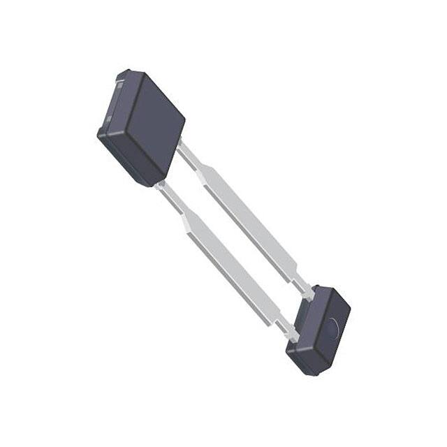
Package: 2-Pin SIP (Suffix UB)
The A1699 is provided in a 2-pin miniature SIP package
(suffix UB) that is lead (Pb) free, with tin leadframe plating.
The UB package includes an IC and capacitor integrated into a
single overmolded package to reduce external EMI protection
requirements.
The IC employs patented algorithms for the special operational
requirements of automotive transmission applications. The
speed and direction of the target are communicated through a
variable pulse-width output protocol. The A1699 is particularly
adept at handling vibration without sacrificing maximum air
gap capability or creating any erroneous direction information.
The advanced vibration detection algorithm will systematically
calibrate the sensor IC on the initial magnetic poles of true
target rotation and not on vibration, always guaranteeing an
accurate signal in running mode.
Advanced signal processing and innovative algorithms make
the A1699 an ideal solution for a wide range of speed- and
direction-sensing needs.
Not to scale
VCC
Regulator
(Analog)
Regulator
(Digital)
Hall Amp
Offset
Adjust
AGC
Filter
ADC
Synchronous
Digital Controller
Hall Amp
Offset
Adjust
AGC
Filter
Output
Control
ADC
GND
Functional Block Diagram
A1699-DS, Rev. 8
MCO-0000636
April 3, 2019
�Two-Wire, Differential, Vibration-Resistant
Sensor IC with Speed and Direction Output
A1699
Complete Part
Number Format
Configuration
A1699 L UB TN -X X X X X -T
Allegro Identifier and Device Type
Operating Temperature Range
Package Designation
Instructions (Packing)
Leadframe Plating
Allegro Identifier and Device Type
[A1699]
Operating Temperature Range
[L]
Package Designation
[UB] 2-pin plastic SIP
Instructions (Packing)
[TN] Tape and reel
Configuration
Rotation Direction
[-F] pin 1-to-2 forward or
[-R] pin 2-to-1 forward
Number of Pulses
[S] single, one pulse per magnetic pole pair or
[D] dual, one pulse for each north and south pole
Reverse Pulse
Width
[N] 90 µs (narrow) or
[W] 180 µs (wide)
Calibration Pulses
[B] Blanked, no output during Calibration or
[P] Pulses during Calibration
Vibration Immunity
/ Direction Change
[L] Low vibration immunity with immediate
direction change detection or
[H] High vibration immunity with non-direction
pulses
Leadframe Plating
[T] Lead (Pb) free
For example: A1699LUBTN-RSNPL-T
Where a configuration character is unspecified, “x” will be used. For example, -xSNPL applies to both
Rotation Direction configuration variants.
Allegro MicroSystems
955 Perimeter Road
Manchester, NH 03103-3353 U.S.A.
www.allegromicro.com
2
�Two-Wire, Differential, Vibration-Resistant
Sensor IC with Speed and Direction Output
A1699
SELECTION GUIDE
Part Number
Packing*
A1699LUBTN–xxxxx–T
4000 pieces per 13-in. reel
*Contact Allegro™ for additional packing options.
ABSOLUTE MAXIMUM RATINGS*
Characteristic
Symbol
Supply Voltage
VCC
Reverse Supply Voltage
VRCC
Rating
Unit
28
V
–18
V
–40 to 150
ºC
TJ(max)
165
ºC
Tstg
–65 to 170
ºC
Value (Typ.)
Unit
10000
pF
Operating Ambient Temperature
TA
Maximum Junction Temperature
Storage Temperature
Notes
Refer to Power Derating Section
L temperature range
INTERNAL DISCRETE CAPACITOR RATINGS
Characteristic
Symbol
Nominal Capacitance
CSUPPLY
Test Conditions
Connected between VCC and GND
Terminal List Table
1
Name
Number
Function
VCC
1
Supply Voltage
GND
2
Ground
2
Package UB, 2-Pin SIP Pinout Diagram
Allegro MicroSystems
955 Perimeter Road
Manchester, NH 03103-3353 U.S.A.
www.allegromicro.com
3
�Two-Wire, Differential, Vibration-Resistant
Sensor IC with Speed and Direction Output
A1699
OPERATING CHARACTERISTICS: Valid throughout full operating and temperature ranges, unless otherwise specified
Characteristic
Symbol
Test Conditions
Min.
Typ.1
Max.
Unit
ELECTRICAL CHARACTERISTICS
Supply Voltage2
Undervoltage Lockout
VCC
Operating, TJ < TJ(max)
4
–
24
V
VCC transitioning from 0 → 5 V or 5 → 0 V
–
3.6
3.95
V
VCC = VRCC(max)
–
–
–10
mA3
VZSUPPLY
ICC = ICC(max) + 3 mA, TA = 25ºC
28
–
–
V
ICC(LOW)
Low-current state (running mode)
5
–
8
mA
ICC(HIGH)
High-current state (running mode)
12
–
16
mA
Low-current level (calibration) and Power-on
mode
5
–
8.5
mA
1.9
–
–
–
VCC(UV)
Reverse Supply Current3
Supply Zener Clamp Voltage
Supply Current
IRCC
ICC(SU)
(LOW)
Supply Current Ratio
ICC(HIGH)/
ICC(LOW)
Measured as a ratio of high current to low
current
OUTPUT
Output Rise Time
tr
ΔI/Δt from 10% to 90% ICC level; Corresponds to
measured output slew rate with CSUPPLY
–
2
4
μs
Output Fall Time
tf
ΔI/Δt from 90% to 10% ICC; Corresponds to
measured output slew rate with CSUPPLY
–
2
4
μs
OUTPUT PULSE CHARACTERISTICS4
Pulse Width, Forward Rotation
Pulse Width, Reverse Rotation
Pulse Width, Non-Direction
tw(FWD)
tw(REV)
tw(ND)
38
45
52
μs
-xxNxx variant
76
90
104
μs
-xxWxx variant
153
180
207
μs
-xxNPx and -xxNxH variants
153
180
207
μs
-xxWPx and -xxWxH variants
306
360
414
μs
Continued on the next page…
VS
1 VCC
CSUPPLY
A1699
2 GND
VOUT
CL
RL
Figure 1: Typical Application Circuit
Allegro MicroSystems
955 Perimeter Road
Manchester, NH 03103-3353 U.S.A.
www.allegromicro.com
4
�Two-Wire, Differential, Vibration-Resistant
Sensor IC with Speed and Direction Output
A1699
OPERATING CHARACTERISTICS (continued): Valid throughout full operating and temperature ranges, unless otherwise
specified
Characteristic
Symbol
Test Conditions
Min.
Typ.1
Max.
Unit
Operate Point
BOP
% of peak-to-peak IC-processed magnetic signal
–
69
–
%
Release Point
BRP
% of peak-to-peak IC-processed magnetic signal
–
31
–
%
-xSxxx variant
0
–
12
kHz
-xDxxx variant
0
–
6
kHz
-xSNxx variant
0
–
7
kHz
-xDNxx variant
0
–
3.5
kHz
OPERATING CHARACTERISTICS
Operating Frequency, Forward
Rotation
fFWD
Operating Frequency, Reverse
Rotation5
fREV
Operating Frquency, Non-Direction
Pulses5
fND
-xSWxx variant
0
–
4
kHz
-xDWxx variant
0
–
2
kHz
-xSNxx variant
0
–
4
kHz
-xDNxx variant
0
–
2
kHz
-xSWxx variant
0
–
2.2
kHz
-xDWxx variant
0
–
1.1
kHz
Magnitude valid for both differential magnetic
channels
–300
–
300
G
Peak to peak differential signal; valid for each
magnetic channel.
30
–
1200
G
-xxxxL variant
TTARGET
–
–
deg.
-xxxxH variant
TTARGET
–
–
deg.
-xxxxL variant
0.12 ×
TTARGET
–
–
deg.
-xxxxH variant
TTARGET
–
–
deg.
–
–0.2
–
%/°C
DAC CHARACTERISTICS
Allowable User-Induced Offset
PERFORMANCE CHARACTERISTICS
Operational Magnetic Range
BIN
Vibration Immunity (Startup)
ErrVIB(SU)
See Figure 2
Vibration Immunity (Running Mode)
ErrVIB
See Figure 2
Magnetic Temperature Coefficient
TCMAG
Optimized value, for ring magnet
1 Typical
values are at TA = 25°C and VCC = 12 V. Performance may vary for individual units, within the specified maximum and minimum limits.
voltage must be adjusted for power dissipation and junction temperature; see representative discussions in Power Derating section.
3 Negative current is defined as conventional current coming out of (sourced from) the specified device terminal.
4 Load circuit is RL = 100 Ω and CL = 10 pF. Pulse duration measured at threshold of ( (I
CC(HIGH) + ICC(LOW)) /2).
5 Maximum Operating Frequency is determined by satisfactory separation of output pulses: I
CC(LOW) of tw(FWD)(MIN). If the customer can resolve shorter low-state durations,
maximum fREV and fND may be increased.
2 Maximum
Target
S
N
S
360º (degrees prime)
N
VSP
T TARGET
VPROC
VPROC(BOP)
TVPROC
VPROC(pk-pk)
VPROC = the processed analog signal of the sinusoidal magnetic input (per channel)
TTARGET = the period between successive sensed target magnetic edges of the same
polarity (either both north-to-south or both south-to-north)
(BOP)
(BRP)
VPROC(BRP)
VSP
VSP(sep) =
VSP
VPROC(pk-pk)
Figure 2: Definition of TTARGET
Allegro MicroSystems
955 Perimeter Road
Manchester, NH 03103-3353 U.S.A.
www.allegromicro.com
5
�Two-Wire, Differential, Vibration-Resistant
Sensor IC with Speed and Direction Output
A1699
OPERATING CHARACTERISTICS (continued): Valid throughout full operating and temperature ranges, unless otherwise
specified
Characteristic
Symbol
Test Conditions
Min.
Typ.1
Max.
Unit
INPUT MAGNETIC CHARACTERISTICS
Allowable Differential Sequential
Signal Variation
BSEQ(n+1) /
BSEQ(n)
Signal cycle-to-cycle variation (see Figure 3)
0.6
–
–
–
BSEQ(n+i) /
BSEQ(n)
Overall signal variation (see Figure 3)
0.4
–
–
–
BIN > 60 GPP
BIN ≤ 1200 GPP
–
2×
TTARGET
很抱歉,暂时无法提供与“A1699LUBTN-FSWPH-T”相匹配的价格&库存,您可以联系我们找货
免费人工找货