A17301
Three-Wire Zero-Speed Differential Peak-Detecting
Sensor IC with Continuous Calibration
FEATURES AND BENEFITS
DESCRIPTION
• Immune to common external magnetic disturbance
• Operates down to 20 Gpk-pk differential input field for
large air gaps or small back-biasing fields
• Running mode recalibration after start-up vibration
ensures immunity to possible target anomalies
• Accurate duty cycle on output signal throughout
operating temperature range and air gaps
• Integrated capacitors for EMC performance
The A17301 integrates a single IC and EMC components into
a small SIP package, providing a robust and cost-effective
solution for digital ring-magnet sensing or ferromagnetic target
sensing when coupled with a back-biasing magnet. The device
can be used in two-wheeled vehicle applications where a wide
variety of target shapes and sizes are used.
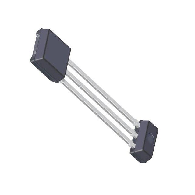
PACKAGE:
3-pin SIP (suffix UC)
The integrated circuit incorporates dual Hall-effect elements
with 2.2 mm spacing and signal processing that switches in
response to differential magnetic signals created by ringmagnet poles. The circuitry contains a sophisticated digital
circuit to reduce system offsets, to calibrate the gain for airgap-independent switchpoints, and to achieve true zero-speed
operation. Running mode recalibration provides immunity to
environmental effects such as micro-oscillations of the target
or sudden air gap changes. Use of a digital peak detector for
output switching control ensures the input signal is never lost,
regardless of the amount of signal shift between output edges.
The A17301 is ideally suited to obtain speed and duty cycle
information for position and timing applications, such as in
speedometers/tachometers.
The A17301 is available in a 3-pin SIP (suffix UC). The package
is lead (Pb) free, with 100% matte-tin leadframe plating.
Not to scale
VCC
E1
Hall
Amplifier
∑
Internal
Regulator
Gain
E2
Automatic Offset
Adjustment (AOA)
Control
AOA DAC
Automatic Gain
Control (AGC)
AGC DAC
Tracking DAC
Peak Hold
OUT
+
–
Current
Limit
GND
Figure 1: Functional Block Diagram
A17301-DS, Rev. 1
MCO-0000513
October 25, 2019
�Three-Wire Zero-Speed Differential Peak-Detecting
Sensor IC with Continuous Calibration
A17301
SELECTION GUIDE
[1]
Part Number
Package
Packing [1]
Operating Ambient
Temperature Range, TA (°C)
A17301PUCFTN
3-pin SIP
13-inch tape and reel, 4000 pieces per reel
–40 to 160
Contact Allegro™ for additional packing options.
ABSOLUTE MAXIMUM RATINGS
Characteristic
Symbol
Forward Supply Voltage
VCC
Reverse Supply Voltage
VRCC
Notes
Rating
Refer to Power Derating Curves chart
Unit
38
V
–18
V
Output Current
IOUT
30
mA
Reverse Output Current
IROUT
–50
mA
Reverse Output Voltage
VROUT
–0.5
V
Output Off Voltage
VOUT
28
V
Operating Ambient Temperature
TA
–40 to 160
°C
Maximum Junction Temperature
TJ(max)
175
°C
Tstg
–65 to 170
°C
Storage Temperature
P temperature range
VSUPPLY*
UC Package, 3-Pin SIP
Pinout Diagram
Branded
Face
RPULLUP
A17301
3
OUT
1
VCC
Sensor
Output
COUT
CBYP
1
2
3
2 GND
*As shown, VSUPPLY = VPULLUP; device allows
for independent VPULLUP voltage if desired.
Figure 2: Typical Application Circuit
TERMINAL LIST
INTERNAL COMPONENT LIST
Number
Name
Description
1
VCC
Supply voltage
Name
Reference
Nominal Value
Bypass Capacitor
CBYP
100 nF
2
GND
Ground
Output Capacitor
COUT
1.8 nF
3
OUT
Open drain output
Allegro MicroSystems
955 Perimeter Road
Manchester, NH 03103-3353 U.S.A.
www.allegromicro.com
2
�Three-Wire Zero-Speed Differential Peak-Detecting
Sensor IC with Continuous Calibration
A17301
OPERATING CHARACTERISTICS: Valid throughout operating voltage and ambient temperature ranges, typical data
applies at VCC = 12 V and TA = 25°C, unless otherwise specified
Characteristics
Symbol
Test Conditions
Min.
Typ.
Max.
Unit [1]
Operating, TJ ≤ TJ(max)
4
–
26.5
V
VCC = 0 → VCC(min) + 1 V and
VCC(min) + 1 V → 0 V
–
–
4
V
VCC > VCC(min)
3
5
7.5
mA
VOUT, connected as in Figure 2
–
High
–
V
VCC > VCC(min)
–
–
2.3
ms
ELECTRICAL CHARACTERISTICS
Supply Voltage [2]
VCC
Undervoltage Lockout
VCC(uv)
Supply Current
ICC
POWER-ON CHARACTERISTICS
Power-On State
POS
Power-On Time [3]
tPO
TRANSIENT PROTECTION CHARACTERISTICS
Supply Zener Clamp Voltage
VZ(supply)
ICC = ICC(max) + 3 mA, TA = 25 °C
38
–
–
V
Supply Zener Current
IZ(supply)
VCC = 38 V
–
–
ICC(max) + 3
mA
Reverse Supply Current
IRCC
VRCC = –18 V, TJ < TJ(max)
–1
–
–
mA
VZ(output)
IOUT = 3 mA, TA = 25°C
28
–
–
V
Output Zener Current
IZ(output)
VOUT = 28 V
Output Current Limit
IOUT(lim)
Output Zener Clamp Voltage
–
–
3
mA
30
–
85
mA
IOUT(sink) = 20 mA
–
220
400
mV
VOUT = 24 V, output off
–
–
10
µA
90% → 10%, VPULLUP = 12 V, RPULLUP = 1 kΩ
–
1.7
–
µs
20
–
1200
G
–
120
–
mV
3
–
10
G
–
120
–
mV
3
–
10
G
OUTPUT STAGE CHARACTERISTICS
Output Saturation Voltage
VOUT(sat)
Output Leakage Current
IOFF
Output Fall Time
tf
PERFORMANCE CHARACTERISTICS
Operating Magnetic Signal Range
BDIFF
Peak-to-peak of differential signal; operation
within specification
Operate Point [4]
BOP
See Figure 8
Release Point [4]
BRP
See Figure 8
Operating Frequency
fOP
0
–
10
kHz
Analog Signal Bandwidth
BW
Equivalent to f = –3 dB
20
–
–
kHz
Initial Calibration Cycle [5]
ncal
Output rising edges before calibration is
completed, 0 G offset, fOP ≤ 200 Hz
–
–
3
edge
Output Duty Cycle Precision
DOUT
Using a pure sine magnetic signal, with fOP and
BDIFF within specification
–
–
±15
%
Output Period Precision
TOUT
Using pure sine magnetic signal with
BDIFF = 50 Gpk-pk and fOP = 1 kHz
–
0.3
–
%
Output switching only
–
–
±100
G
Allowable User-Induced Differential
Offset
BDIFFEXT
[1] 1 G
(gauss) = 0.1 mT (millitesla).
voltage operation must not exceed maximum junction temperature. Refer to Power Derating Curves chart.
[3] Time required to initialize device. Power-On Time includes the time required to complete the internal automatic offset adjust. The DAC is then ready for peak acquisition.
[4] Values in G are based on device in maximum gain setting.
[5] Non-uniform magnetic profiles may require additional output pulses before calibration is complete.
[2] Maximum
Allegro MicroSystems
955 Perimeter Road
Manchester, NH 03103-3353 U.S.A.
www.allegromicro.com
3
�Three-Wire Zero-Speed Differential Peak-Detecting
Sensor IC with Continuous Calibration
A17301
THERMAL CHARACTERISTICS: May require derating at maximum conditions; see application information
Characteristic
Package Thermal Resistance
Test Conditions [1]
Value
Unit
270
°C/W
On single-layer PCB with copper limited to solder pads
RθJA
thermal information available on the Allegro website.
Power Derating Curve
28
26
VCC(max)
Maximum Allowable VCC (V)
24
22
20
18
16
14
1-layer PCB, Package UC
(RθJA = 270°C/W)
12
10
8
6
VCC(min)
4
2
20
40
60
80
100
120
140
160
180
Temperature (°C)
Power Dissipation versus Ambient Temperature
800
700
Power Dissipation, PD (mW)
[1] Additional
Symbol
600
1-layer PCB, Package UC
(RθJA = 270°C/W)
500
400
300
200
100
0
20
40
60
80
100
120
140
160
180
Temperature (°C)
Allegro MicroSystems
955 Perimeter Road
Manchester, NH 03103-3353 U.S.A.
www.allegromicro.com
4
�Three-Wire Zero-Speed Differential Peak-Detecting
Sensor IC with Continuous Calibration
A17301
CHARACTERISTIC PERFORMANCE
Supply Current Over VCC and Temperature
Output On (VOUT = Low)
7
6
5
VCC (V)
4
4
3
12
2
26
1
0
-50
0
50
100
150
Supply Current, ICC (mA)
Supply Current, ICC (mA)
Supply Current Over Temperature and VCC
Output On (VOUT = Low)
7
6
5
T A (°C)
4
-40
3
25
2
160
1
0
200
0
5
10
7
6
VCC (V)
4
4
3
12
2
26
1
0
-50
0
50
100
150
200
30
6
5
T A (°C)
4
-40
3
25
2
160
1
0
0
5
10
15
20
25
30
Supply Voltage (VCC )
Output Saturation Voltage Over Temperature
Output Fall Time Over Temperature
500
3
450
2.5
400
350
300
IOUT (mA)
250
200
20
150
100
Fall Time (µs)
Saturation Voltage (mV)
25
7
Ambient Temperature (°C)
2
1.5
VPULLUP, RPULLUP
12 V, 1 kΩ
1
0.5
50
0
20
Supply Current Over VCC and Temperature
Output Off (VOUT = High)
Supply Current, ICC (mA)
Supply Current, ICC (mA)
Supply Current Over Temperature and VCC
Output Off (VOUT = High)
5
15
Supply Voltage (VCC )
Ambient Temperature (°C)
-50
0
50
100
Ambient Temperature (°C)
150
200
0
-50
0
50
100
150
200
Ambient Temperature (°C)
Allegro MicroSystems
955 Perimeter Road
Manchester, NH 03103-3353 U.S.A.
www.allegromicro.com
5
�Three-Wire Zero-Speed Differential Peak-Detecting
Sensor IC with Continuous Calibration
A17301
CHARACTERISTIC PERFORMANCE (continued)
Duty Cycle Error Over Temperature
At 1 mm Air Gap*
16
16
14
14
12
10
T A (°C)
8
-40
6
25
4
160
2
0
0
0.5
1
1.5
2
Duty Cycle Error (%)
Duty Cycle Error (%)
Duty Cycle Error Over Operating Frequency
At 1 mm Air Gap*
12
0.5
8
1
6
1.5
4
2
2
0
2.5
fOP (kHz)
10
-50
0
Opearating Frequency (kHz)
16
14
14
12
10
T A (°C)
8
-40
6
25
4
160
2
0.5
1
1.5
2
Air Gap* (mm)
2.5
3
3.5
Duty Cycle Error (%)
Duty Cycle Error (%)
16
0
100
150
200
Duty Cycle Error Over Temperature
At 1 kHz Operating Frequency
Duty Cycle Error Over Air Gap
At 1 kHz Operating Frequency
0
50
Ambient Temperature (°C)
Air Gap* (mm)
12
0.5
10
1
8
1.5
6
2
4
2.5
2
0
3
-50
0
50
100
150
200
Ambient Temperature (°C)
*Air gap defined as the distance between the front face of the A17301 package to the ring magnet target.
Allegro MicroSystems
955 Perimeter Road
Manchester, NH 03103-3353 U.S.A.
www.allegromicro.com
6
�Three-Wire Zero-Speed Differential Peak-Detecting
Sensor IC with Continuous Calibration
A17301
CHARACTERISTIC ALLOWABLE AIR GAP MOVEMENT
Allowable Air Gap Movement from TEAGCAL*
2.0
∆TEAGOUT (mm)
1.5
1.0
0.5
0
-0.5
-1.0
0
0.5
1.0
1.5
2.0
∆TEAGIN (mm)
2.5
3.0
3.5
*Data based on study performed using Allegro Reference
ring magnet target, and applicable to ring magnet targets
with similar magnetic characteristics.
The colored area in the chart above shows the region of allowable air gap movement within which the device will continue
output switching. The output duty cycle is wholly dependent on
the target’s magnetic signature across the air gap range of movement and may not always be within specification throughout the
entire operating region (to AG(OPmax)).
The axis parameters for the chart are defined in Figure 3. As
an example, assume the case where the air gap is allowed to
vary from the nominal installed air gap (TEAGCAL , Figure 3,
(a)
panel a) within the range defined by an increase of ΔTEAGOUT =
0.35 mm (Figure 3, panel b), and a decrease of ΔTEAGIN =
0.65 mm (Figure 3, panel c). This case is plotted with an “x” in
the chart above.
Note that after extreme cases of decrease in air gap, the device
may not switch when the air gap resumes the nominal value. For
example, if ΔTEAGIN = 2.75 mm, the chart shows ΔTEAGOUT
= –0.5 mm, meaning that the device can now switch only in the
air gap range of 0.5 to 2.75 mm inward from the nominal air gap.
(b)
(c)
TEAGCAL
TEAG OUT
TEAG IN
Figure 3
Allegro MicroSystems
955 Perimeter Road
Manchester, NH 03103-3353 U.S.A.
www.allegromicro.com
7
�A17301
Three-Wire Zero-Speed Differential Peak-Detecting
Sensor IC with Continuous Calibration
FUNCTIONAL DESCRIPTION
Sensing Technology
The single-chip differential Hall-effect sensor IC possesses two
Hall elements that sense the magnetic profile of the ring magnet
simultaneously but at different points (spaced at a 2.2 mm pitch),
generating a differential internal analog voltage, VPROC , that is
processed for precise switching of the digital output signal, as
shown in Figure 4.
The Hall IC is self-calibrating and also possesses a temperaturecompensated amplifier and offset compensation circuitry. Its
voltage regulator provides supply noise rejection throughout the
operating voltage range. Changes in temperature do not greatly
affect this device due to the stable amplifier design and the offset
compensation circuitry. The Hall transducers and signal processing electronics are integrated on the same silicon substrate, using
a proprietary BiCMOS process.
Target
(Ring Magnet)
S
S
N
N
Element Pitch
Hall Element 2
Hall Element 1
Hall IC
(Pin 3 Side)
(Pin 1 Side)
Figure 4: Relative Motion of the Target
The relative motion of the target is detected by the dual Hall elements
mounted on the Hall IC.
Target Profiling
An operating device is capable of providing digital information
that is representative of the magnetic features on a rotating target.
The waveform diagram shown in Figure 6 presents the automatic
translation of the magnetic profile to the digital output signal of
the device.
Output Polarity
Figure 6 shows the output polarity for the orientation of target
and device shown in Figure 5. The target direction of rotation
shown is: perpendicular to the leads, across the face of the device,
from the pin 1 side to the pin 3 side. This results in the device
output switching from low to high as the leading edge of a north
magnetic pole passes the device face. In this configuration, the
device output voltage switches to its high polarity when a north
pole is the target feature nearest to the device. If the direction of
rotation is reversed, then the output polarity inverts.
Forward Rotation
S
Rotating Target
(Ring magnet or
ferromagnetic)
Reverse Rotation
Branded Face
of UC Package
N
S N
S NS
N
Pin 1
Pin 3
Figure 5: Target Rotation
Branded Face
of UC Package
This left-to-right (pin 1 to pin 3) direction of target rotation
results
in a high output signal when a target north pole is nearest the face
N
S
of the device (see
Figure 6). A right-to-left
(pin 3 to pin 1) rotation
S
N S
N
S N
Rotating Target inverts the output signal polarity.
(Ring magnet or
ferromagnetic)
Pin 1
Pin 3
Allegro MicroSystems
955 Perimeter Road
Manchester, NH 03103-3353 U.S.A.
www.allegromicro.com
8
�Three-Wire Zero-Speed Differential Peak-Detecting
Sensor IC with Continuous Calibration
A17301
S
N
VPROC = LEFT-RIGHT
S
Left
Right
pin 3
pin 1
OUTPUT
TIME
S
N
VPROC = LEFT-RIGHT
S
Left
Right
pin 3
pin 1
OUTPUT
TIME
S
N
VPROC = LEFT-RIGHT
S
Left
Right
pin 3
pin 1
OUTPUT
TIME
VPROC = LEFT-RIGHT
S
N
Left
pin 1
S
Right
pin 3
OUTPUT
TIME
Figure 6: Output Profile of a Ring Magnet Target from Pin 1 to Pin 3 (as indicated in Figure 5)
Allegro MicroSystems
955 Perimeter Road
Manchester, NH 03103-3353 U.S.A.
www.allegromicro.com
9
�A17301
Three-Wire Zero-Speed Differential Peak-Detecting
Sensor IC with Continuous Calibration
Automatic Gain Control (AGC)
This feature allows the device to operate with an optimal internal
electrical signal, regardless of the differential signal amplitude
(within the BDIFF and BDIFFEXT specifications). During calibration, the device determines the peak-to-peak amplitude of the
signal generated by the target. The gain of the device is then automatically adjusted. Figure 7 illustrates the effect of this feature.
During running mode, the AGC continues to monitor the system
amplitude, reducing the gain if necessary; see the Device Operation section for more details.
Target
Ring Magnet
Digital Peak Detection
A DAC tracks the internal analog voltage signal, VPROC, and is
used for holding the peak value of the internal analog signal. In
the example shown in Figure 8, the DAC would first track up
with the signal and hold the upper peak’s value. When VPROC
drops below this peak value by BOP , the device hysteresis, the
output would switch and the DAC would begin tracking the signal downward toward the negative VPROC peak. After the DAC
acquires the negative peak, the output will again switch states
when VPROC is greater than the peak by the value BRP . At this
point, the DAC tracks up again and the cycle repeats. The digital
tracking of the differential analog signal allows the device to
achieve true zero-speed operation.
S
N
S
Internal Differential
Analog Signal
Response, without AGC
AGLarge
AGSmall
V+
Automatic Offset Adjust (AOA)
The AOA is patented circuitry that automatically compensates for
the effects of chip, magnet, and installation offsets. This circuitry
is continuously active, including both during calibration mode
and running mode, compensating for offset drift. Continuous
operation also allows it to compensate for offsets induced by
temperature variations over time.
N
V+
Internal Differential
Analog Signal
Response, with AGC
AGSmall
AGLarge
Figure 7: Automatic Gain Control (AGC)
The AGC function corrects for variances in the air gap. Differences in
the air gap affect the magnetic gradient, but AGC prevents that from
affecting device performance, as shown in the lowest panel.
V+
Internal
Differential
Analog Signal,
VPROC
0
BOP
BOP
BRP
BRP
V–
VCC
Device Output,
VOUT
VOUT(sat)
Figure 8: Differential Signal Peaks
The peaks in the resulting differential signal are used to set the
operate (BOP ) and release (BRP ) switchpoints.
Allegro MicroSystems
955 Perimeter Road
Manchester, NH 03103-3353 U.S.A.
www.allegromicro.com
10
�A17301
Three-Wire Zero-Speed Differential Peak-Detecting
Sensor IC with Continuous Calibration
Power Supply Protection
The device contains an on-chip regulator and can operate
throughout a wide VCC range. For devices that must be operated
from an unregulated power supply, transient protection must be
added externally. For applications using a regulated line, EMI/
RFI protection may still be required. Contact Allegro for information on the circuitry required for compliance with various
EMC specifications. Refer to Figure 2 for an example of a basic
application circuit.
Undervoltage Lockout
When the supply voltage falls below the undervoltage lockout
voltage, VCC(uv) , the device enters Reset, where the output state
returns to the Power-On State (POS) until sufficient VCC
is supplied.
Assembly Description
This device is integrally molded into a plastic body that has been
optimized for size, ease of assembly, and manufacturability. High
operating temperature materials are used in all aspects of construction.
Device Operation
Each operating mode is described in detail below.
POWER-ON
When power (VCC > VCC(min)) is applied to the device, a short
period of time is required to power the various portions of the IC.
During this period, the A17301 powers-on in the high-voltage
state, VOUT = VPULLUP , and the digital tracking DAC gets ready
to track the VPROC signal. After power-on, there are conditions
that could induce a change in the output state. Such an event
could be caused by thermal transients, but would require a static
applied magnetic field, proper signal polarity, and particular
direction and magnitude of internal signal drift.
INITIAL OFFSET ADJUST
The device initially cancels the effects of chip, magnet, and
installation offsets. After offsets have been cancelled, the device
is ready to provide the first output switch. The period of time
required for both Power-On and Initial Offset Adjust is defined as
the Power-On Time.
CALIBRATION MODE
The calibration mode allows the device to automatically select
the proper signal gain and continue to adjust for offsets. The
AGC is active and selects the optimal signal gain based on the
amplitude of the VPROC signal. Following each adjustment to the
AGC DAC, the Offset DAC is also adjusted to ensure the internal
analog signal is properly centered.
During this mode, the tracking DAC is active and output switching occurs, but the duty cycle is not guaranteed to be within
specification.
RUNNING MODE
After the Initial Calibration period, the device establishes a signal
gain and then transitions into running mode. During running
mode, the device tracks the input signal and gives an output edge
for every peak of the signal. AOA remains active to compensate
for any offset drift over time.
Allegro MicroSystems
955 Perimeter Road
Manchester, NH 03103-3353 U.S.A.
www.allegromicro.com
11
�Three-Wire Zero-Speed Differential Peak-Detecting
Sensor IC with Continuous Calibration
A17301
The A17301 incorporates an algorithm for adjusting the signal
gain during running mode. This algorithm is designed to optimize
the VPROC signal amplitude in instances where the magnetic
signal “seen” during the calibration period is not representative
of the amplitude of the magnetic signal for the installed device
1
2
air gap (see Figure 9). Note that in this mode, the gain can be
reduced but not increased, so this algorithm applies only to
instances in which the magnetic signal amplitude during running
is higher than that during calibration.
3
4
5
BOP
Internal Differential
Signal, VPROC
BOP
BRP
BRP
Device Electrical
Output, VOUT
Figure 9: Operation of Running Mode Gain Adjust
• Position1: The device is initially powered-on. Self-calibration occurs.
• Position 2: Small amplitude oscillation of the target sends an erroneously small differential signal to the device. The amplitude of VPROC is greater than
the switching hysteresis (BOP and BRP), and the device output switches.
• Position 3: The calibration period completes on the third rising output edge, and the device enters running mode.
• Position 4: True target rotation occurs and the correct magnetic signal is generated for the installation air gap. The established signal gain is too large
for the target rotational magnetic signal at the given air gap.
• Position 5: Running mode calibration corrects the signal gain to an optimal level for the installation air gap.
Allegro MicroSystems
955 Perimeter Road
Manchester, NH 03103-3353 U.S.A.
www.allegromicro.com
12
�Three-Wire Zero-Speed Differential Peak-Detecting
Sensor IC with Continuous Calibration
A17301
POWER DERATING
The device must be operated below the maximum junction
temperature of the device, TJ(max). Under certain combinations of
peak conditions, reliable operation may require derating supplied
power or improving the heat dissipation properties of the application. This section presents a procedure for correlating factors
affecting operating TJ. (Thermal data is also available on the
Allegro MicroSystems website.)
The Package Thermal Resistance, RθJA, is a figure of merit summarizing the ability of the application and the device to dissipate
heat from the junction (die), through all paths to the ambient air.
Its primary component is the Effective Thermal Conductivity, K,
of the printed circuit board, including adjacent devices and traces.
Radiation from the die through the device case, RθJC, is relatively
small component of RθJA. Ambient air temperature, TA, and air
motion are significant external factors, damped by overmolding.
The effect of varying power levels (Power Dissipation, PD), can
be estimated. The following formulas represent the fundamental
relationships used to estimate TJ, at PD.
PD = VIN × IIN
ΔT = PD × RθJA
Example: Reliability for VCC at TA = 160°C, package UC, using
single-layer PCB.
Observe the worst-case ratings for the device, specifically:
RθJA = 270°C/W, TJ(max) = 175°C, VCC(max) = 26.5 V, and
ICC(max) = 7.5 mA.
Calculate the maximum allowable power level, PD(max). First,
invert equation 3:
ΔTmax = TJ(max) – TA = 175°C – 160 °C = 15 °C
This provides the allowable increase to TJ resulting from internal
power dissipation. Then, invert equation 2:
PD(max) = ΔTmax ÷ RθJA = 15°C ÷ 270°C/W = 55.6 mW
Finally, invert equation 1 with respect to voltage:
(1)
VCC(est) = PD(max) ÷ ICC(max) = 55.6 mW ÷ 7.5 mA = 7.41 V
(2)
The result indicates that, at TA, the application and device can
dissipate adequate amounts of heat at voltages ≤VCC(est).
TJ = TA + ΔT (3)
For example, given common conditions such as: TA= 25°C,
VCC = 12 V, ICC = 5 mA, and RθJA = 270°C/W, then:
A worst-case estimate, PD(max), represents the maximum allowable power level (VCC(max) , ICC(max)), without exceeding TJ(max),
at a selected RθJA and TA.
Compare VCC(est) to VCC(max). If VCC(est) ≤ VCC(max), then reliable operation between VCC(est) and VCC(max) requires enhanced
RθJA. If VCC(est) ≥ VCC(max), then operation between VCC(est) and
VCC(max) is reliable under these conditions.
PD = VCC × ICC = 12 V × 5 mA = 60 mW
ΔT = PD × RθJA = 60 mW × 270°C/W = 16.2°C
TJ = TA + ΔT = 25°C + 16.2°C = 41.2°C
Allegro MicroSystems
955 Perimeter Road
Manchester, NH 03103-3353 U.S.A.
www.allegromicro.com
13
�Three-Wire Zero-Speed Differential Peak-Detecting
Sensor IC with Continuous Calibration
A17301
PACKAGE OUTLINE DIAGRAM
For Reference Only – Not for Tooling Use
(Reference DWG-0000409, Rev. 3)
Dimensions in millimeters – NOT TO SCALE
Dimensions exclusive of mold flash, gate burrs, and dambar protrusions
Exact case and lead configuration at supplier discretion within limits shown
0.545 REF× 2
1.36 REF
B
+0.05
0.10
–0.10
0.15 REF
4×10°
+0.06
4.00
–0.05
0.25 REF × 4
Detail A
1.50 ±0.05
2.20
C
Detail A
2.00
4.00
+0.06
–0.07
E E1
Mold Ejector
Pin Indent
E E2
Branded
Face
45°
R 0.20 All Corners
A
0.25 REF
0.85 ±0.05
0.42 ±0.05
0.30 REF
XXXXX
Date Code
Lot Number
1.27 REF × 2
1
18.00 ±0.10
2
F
3
Standard Branding Reference View
Line 1 = Five digit part number
Line 2 = Four digit date code
Line 3 = Characters 5 through 8 of Assembly Lot Number
12.20 ±0.10
0.25
+0.07
–0.03
Plating Included
0.38 REF
A Dambar removal protrusion (12×)
0.25 REF
B
0.85 ±0.05
1.80
C Active Area Depth, 0.38 mm ±0.05 mm
+0.06
–0.07
D
4.00 +0.06
–0.05
Gate and tie burr area
R 0.30 All Corners
1.50 ±0.05
D
Molded Lead Bar to prevent damage to leads during shipment
E
Hall elements, E1 and E2 (not to scale)
F
Branding scale and appearance at supplier discretion
Figure 8: Package UC, 3-Pin SIP
Allegro MicroSystems
955 Perimeter Road
Manchester, NH 03103-3353 U.S.A.
www.allegromicro.com
14
�Three-Wire Zero-Speed Differential Peak-Detecting
Sensor IC with Continuous Calibration
A17301
REVISION HISTORY
Number
Date
–
October 16, 2018
Initial release
Description
1
October 25, 2019
Minor editorial updates
Copyright 2019, Allegro MicroSystems.
Allegro MicroSystems reserves the right to make, from time to time, such departures from the detail specifications as may be required to permit
improvements in the performance, reliability, or manufacturability of its products. Before placing an order, the user is cautioned to verify that the
information being relied upon is current.
Allegro’s products are not to be used in any devices or systems, including but not limited to life support devices or systems, in which a failure of
Allegro’s product can reasonably be expected to cause bodily harm.
The information included herein is believed to be accurate and reliable. However, Allegro MicroSystems assumes no responsibility for its use; nor
for any infringement of patents or other rights of third parties which may result from its use.
Copies of this document are considered uncontrolled documents.
For the latest version of this document, visit our website:
www.allegromicro.com
Allegro MicroSystems
955 Perimeter Road
Manchester, NH 03103-3353 U.S.A.
www.allegromicro.com
15
�