A3282
Chopper-Stabilized Hall-Effect Latch
Discontinued Product
This device is no longer in production. The device should not be
purchased for new design applications. Samples are no longer
available.
Date of status change: July 30, 2010
Recommended Substitutions:
Our next generation recommended substitutes are:
• For the A3282ELHLT-T, we recommend the A1222ELHLX-T.
• For the A3282LLHLT-T, we recommend the A1222LLHLX-T.
• For the A3282LUA-T, we recommend the A1222LUA-T.
NOTE: For detailed information on purchasing options, contact your
local Allegro field applications engineer or sales representative.
Allegro MicroSystems, Inc. reserves the right to make, from time to time, revisions to the anticipated product life cycle plan
for a product to accommodate changes in production capabilities, alternative product availabilities, or market demand. The
information included herein is believed to be accurate and reliable. However, Allegro MicroSystems, Inc. assumes no responsibility for its use; nor for any infringements of patents or other rights of third parties which may result from its use.
�A3282
Chopper-Stabilized Hall-Effect Latch
Features and Benefits
Description
▪ Chopper stabilization
▫ Superior temperature stability
▫ Extremely low switchpoint drift
▫ Insensitive to physical stress
▪ Reverse battery protection
▪ Output short circuit protection
▪ Solid state reliability
▪ Small size
▪ Robust EMC capability
▪ High ESD ratings (HBM)
The A3282 Hall-effect sensor IC is a temperature stable,
stress-resistant latch. Superior high-temperature performance
is made possible through an Allegro® dynamic offset
cancellation that utilizes chopper-stabilization. This
method reduces the offset voltage normally caused by device
overmolding, temperature dependencies, and thermal stress.
The A3282 complements the current Allegro family of chopperstabilized latching devices.
The A3282 includes the following on a single silicon chip:
voltage regulator, Hall-voltage generator, small-signal
amplifier, chopper stabilization, Schmitt trigger, and a short
circuit protected open-drain output. Advanced BiCMOS wafer
fabrication processing is used to take advantage of low-voltage
requirements, component matching, very low input-offset
errors, and small component geometries.
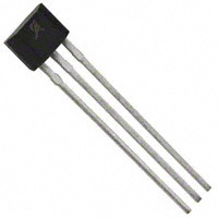
Packages: 3 pin SOT23W (suffix LH), and
3 pin SIP (suffix UA)
This device requires the presence of both south and north
polarity magnetic fields for operation. In the presence of a
south polarity field of sufficient strength, the device output
latches on, and only switches off when a north polarity field
of sufficient strength is present.
Continued on the next page…
Not to scale
Functional Block Diagram
VCC
Regulator
Low-Pass
Filter
Amp
Sample and Hold
Dynamic Offset
Cancellation
To All Subcircuits
VOUT
Control
Current Limit
BOP
–
250
500
mV
Output Current Limit
IOM
B > BOP
30
–
60
mA
Power-On Time
tPO
VCC > 3.6 V
Output On Voltage
–
8
50
μs
–
200
–
kHz
RLOAD = 820 Ω, CS = 20 pF
–
0.2
1
μs
RLOAD = 820 Ω, CS = 20 pF
–
0.2
1
μs
ICCON
B > BOP
–
1.6
3.5
mA
ICCOFF
B < BRP
–
1.6
3.5
mA
VRCC = –18 V
–
–
–2
mA
VZ
ICC = 6.5 mA; TA = 25°C
28
–
–
V
IZ
VS = 28 V
–
–
6.5
mA
BOP
South pole adjacent to branded face of device
70
110
150
G
Release Point
BRP
North pole adjacent to branded face of device
–150
–110
–70
G
Hysteresis
BHYS
BOP – BRP
140
220
300
G
Chopping Frequency
fc
Output Rise Time2
tr
Output Fall Time2
tf
Supply Current
Reverse Battery Current
Supply Zener Clamp Voltage
Supply Zener
Current3
IRCC
Magnetic Characteristics4
Operate Point
1
Maximum voltage must be adjusted for power dissipation and junction temperature, see Power Derating section.
2 C = oscilloscope probe capacitance.
S
3 Maximum current limit is equal to the maximum I
CC(MAX) + 3 mA.
4 Magnetic flux density, B, is indicated as a negative value for north-polarity magnetic fields, and as a positive value for south-polarity magnetic fields.
This so-called algebraic convention supports arithmetic comparison of north and south polarity values, where the relative strength of the field is indicated
by the absolute value of B, and the sign indicates the polarity of the field (for example, a –100 G field and a 100 G field have equivalent strength, but
opposite polarity).
DEVICE QUALIFICATION PROGRAM
Contact Allegro for information.
EMC (Electromagnetic Compatibility) REQUIREMENTS
Contact Allegro for information.
Allegro MicroSystems, Inc.
115 Northeast Cutoff
Worcester, Massachusetts 01615-0036 U.S.A.
1.508.853.5000; www.allegromicro.com
3
�Chopper-Stabilized Hall Effect Latch
A3282
Electrical Characteristic Data
Supply Current (On) versus Ambient Temperature
Supply Current (On) versus Supply Voltage
5.0
5.0
4.0
VCC (V)
3.0
24
3.6
2.0
ICCON (mA)
ICCON (mA)
4.0
1.0
3.0
–40
25
150
2.0
1.0
0
–50
TA (°C)
0
0
50
TA (°C)
100
150
0
25
4.0
VCC (V)
3.0
24
3.6
2.0
ICCOFF (mA)
ICCOFF (mA)
20
5.0
4.0
TA (°C)
–40
25
150
3.0
2.0
1.0
1.0
0
0
0
50
TA (°C)
100
0
150
5
10
15
20
25
VCC (V)
Output Voltage (On) versus Ambient Temperature
Output Voltage (On) versus Supply Voltage
500
500
450
450
400
400
350
350
300
VCC (V)
250
24
3.6
200
150
VOUT(SAT) (mV)
VOUT(SAT) (mV)
15
Supply Current (Off) versus Supply Voltage
5.0
TA (°C)
300
–40
25
150
250
200
150
100
100
50
50
0
–50
10
VCC (V)
Supply Current (Off) versus Ambient Temperature
–50
5
0
0
50
TA (°C)
100
150
0
5
10
15
20
25
VCC (V)
Allegro MicroSystems, Inc.
115 Northeast Cutoff
Worcester, Massachusetts 01615-0036 U.S.A.
1.508.853.5000; www.allegromicro.com
4
�Chopper-Stabilized Hall Effect Latch
A3282
Magnetic Characteristic Data
Operate Point versus Ambient Temperature
150
150
140
140
130
130
VCC (V)
110
24
3.8
100
120
TA (°C)
–40
25
150
BOP (G)
120
BOP (G)
Operate Point versus Supply Voltage
110
100
90
90
80
80
79
79
–50
0
50
TA (°C)
100
150
0
20
25
-80
-80
-90
-90
-100
-100
VCC (V)
-110
24
3.8
-120
TA (°C)
–40
25
150
BRP (G)
BRP (G)
-70
-110
-120
-130
-130
-140
-140
-150
-150
0
50
TA (°C)
100
0
150
5
10
15
20
25
VCC (V)
Hysteresis versus Ambient Temperature
Hysteresis versus Supply Voltage
300
300
280
280
260
260
240
VCC (V)
220
24
3.8
200
BHYS (G)
BHYS (G)
15
Release Point versus Supply Voltage
-70
TA (°C)
240
–40
25
150
220
200
180
180
160
160
140
–50
10
VCC (V)
Release Point versus Ambient Temperature
–50
5
140
0
50
TA (°C)
100
150
0
5
10
15
20
25
VCC (V)
Allegro MicroSystems, Inc.
115 Northeast Cutoff
Worcester, Massachusetts 01615-0036 U.S.A.
1.508.853.5000; www.allegromicro.com
5
�Chopper-Stabilized Hall Effect Latch
A3282
THERMAL CHARACTERISTICS may require derating at maximum conditions, see application information
Characteristic
Symbol
Test Conditions*
RθJA
Package Thermal Resistance
Value Units
Package LH, 1-layer PCB with copper limited to solder pads
228
ºC/W
Package LH, 2-layer PCB with 0.463 in.2 of copper area each side
connected by thermal vias
110
ºC/W
Package UA, 1-layer PCB with copper limited to solder pads
165
ºC/W
*Additional thermal information available on Allegro Web site.
Maximum Allowable VCC (V)
Power Derating Curve
25
24
23
22
21
20
19
18
17
16
15
14
13
12
11
10
9
8
7
6
5
4
3
2
VCC(max)
2-layer PCB, Package LH
(RθJA = 110 ºC/W)
1-layer PCB, Package UA
(RθJA = 165 ºC/W)
1-layer PCB, Package LH
(RθJA = 228 ºC/W)
20
40
60
80
100
VCC(min)
120
140
160
180
Temperature (ºC)
Power Dissipation, PD (m W)
Power Dissipation versus Ambient Temperature
1900
1800
1700
1600
1500
1400
1300
1200
1100
1000
900
800
700
600
500
400
300
200
100
0
2l
(R aye
rP
θJ
C
A =
11 B, P
0 º ac
1-la
C/ ka
W
(R yer PC
) ge L
θJA =
B
H
165 , Pac
ºC/ kage
W)
UA
1-lay
er P
(R
CB,
θJA =
228 Packag
ºC/W
e LH
)
20
40
60
80
100
120
Temperature (°C)
140
160
180
Allegro MicroSystems, Inc.
115 Northeast Cutoff
Worcester, Massachusetts 01615-0036 U.S.A.
1.508.853.5000; www.allegromicro.com
6
�Chopper-Stabilized Hall Effect Latch
A3282
Functional Description
Operation
The output of these devices switches low (turns on) when a
magnetic field perpendicular to the Hall element exceeds the
operate point threshold, BOP. After turn-on, the output voltage
is VOUT(SAT). The output transistor is capable of sinking current
up to the short circuit current limit, IOM, which is a minimum of
30 mA. Note that the device latches, that is, a south pole of sufficient strength towards the branded surface of the device turns the
device on. The device remains on if the south pole is removed.
When the magnetic field is reduced below the release point, BRP ,
the device output turns off (goes high). The difference in the
magnetic operate and release points is the hysteresis, BHYS , of
the device. This built-in hysteresis allows clean switching of the
output even in the presence of external mechanical vibration and
electrical noise.
Powering-on the device in the hysteresis region (less than BOP and
higher than BRP) allows an indeterminate output state. The correct
state is attained after the first excursion beyond BOP or BRP .
Applications
It is strongly recommended that an external bypass capacitor be
connected (in close proximity to the Hall element) between the
supply and ground of the device to reduce both external noise
and noise generated by the chopper stabilization technique. As is
shown in Panel B of figure 1, a 0.1μF capacitor is typical.
Extensive applications information on magnets and Hall-effect
devices is available in:
• Hall-Effect IC Applications Guide, AN27701,
• Hall-Effect Devices: Gluing, Potting, Encapsulating, Lead
Welding and Lead Forming, AN27703.1
• Soldering Methods for Allegro’s Products – SMT and ThroughHole, AN26009
All are provided in Allegro Electronic Data Book, AMS-702 and
the Allegro Web site: www.allegromicro.com
(B)
(A)
VS
V+
VOUT
VCC
Switch to Low
Switch to High
VCC
CBYP
0.1 µF
VOUT(SAT)
0
BOP
B–
BRP
0
A3282
RLOAD
VOUT
Output
GND
B+
BHYS
Figure 1: Switching Behavior of Latches. In Panel A, on the horizontal axis, the B+ direction indicates increasing south polarity magnetic
field strength, and the B– direction indicates decreasing south polarity field strength (including the case of increasing north polarity). This
behavior can be exhibited when using a circuit such as that shown in panel B.
Allegro MicroSystems, Inc.
115 Northeast Cutoff
Worcester, Massachusetts 01615-0036 U.S.A.
1.508.853.5000; www.allegromicro.com
7
�Chopper-Stabilized Hall Effect Latch
A3282
Chopper Stabilization Technique
When using Hall-effect technology, a limiting factor for
switchpoint accuracy is the small signal voltage developed
across the Hall element. This voltage is disproportionally small
relative to the offset that can be produced at the output of the
Hall element. This makes it difficult to process the signal while
maintaining an accurate, reliable output over the specified operating temperature and voltage ranges.
Chopper stabilization is a unique approach used to minimize
Hall offset on the chip. The Allegro technique, namely Dynamic
Quadrature Offset Cancellation, removes key sources of the
output drift induced by thermal and mechanical stresses. This
offset reduction technique is based on a signal modulationdemodulation process. The undesired offset signal is separated
from the magnetic-field-induced signal in the frequency domain,
through modulation. The subsequent demodulation acts as a
modulation process for the offset, causing the magnetic-fieldinduced signal to recover its original spectrum at baseband,
while the dc offset becomes a high-frequency signal. The
magnetic-field-induced signal then can pass through a low-pass
filter, while the modulated dc offset is suppressed. This configuration is illustrated in figure 2.
The chopper stabilization technique uses a 200 kHz highfrequency clock. For demodulation process, a sample and hold
technique is used, where the sampling is performed at twice the
chopper frequency (400 kHz). This high-frequency operation
allows a greater sampling rate, which results in higher accuracy
and faster signal-processing capability. This approach desensitizes the chip to the effects of thermal and mechanical stresses,
and produces devices that have extremely stable quiescent Hall
output voltages and precise recoverability after temperature
cycling. This technique is made possible through the use of a
BiCMOS process, which allows the use of low-offset, low-noise
amplifiers in combination with high-density logic integration and
sample-and-hold circuits.
The repeatability of magnetic-field-induced switching is affected
slightly by a chopper technique. However, the Allegro highfrequency chopping approach minimizes the affect of jitter and
makes it imperceptible in most applications. Applications that
are more likely to be sensitive to such degradation are those
requiring precise sensing of alternating magnetic fields; for
example, speed sensing of ring-magnet targets. For such applications, Allegro recommends its digital device families with lower
sensitivity to jitter. For more information on those devices,
contact your Allegro sales representative.
Regulator
Amp
Low-Pass
Filter
Hall Element
Sample and
Hold
Clock/Logic
Figure 2. Chopper Stabilization Circuit (Dynamic Quadrature Offset Cancellation)
Allegro MicroSystems, Inc.
115 Northeast Cutoff
Worcester, Massachusetts 01615-0036 U.S.A.
1.508.853.5000; www.allegromicro.com
8
�Chopper-Stabilized Hall Effect Latch
A3282
Power Derating
The device must be operated below the maximum junction
temperature of the device, TJ(max). Under certain combinations of
peak conditions, reliable operation may require derating supplied power or improving the heat dissipation properties of the
application. This section presents a procedure for correlating
factors affecting operating TJ. (Thermal data is also available on
the Allegro MicroSystems Web site.)
The Package Thermal Resistance, RJA, is a figure of merit summarizing the ability of the application and the device to dissipate
heat from the junction (die), through all paths to the ambient air.
Its primary component is the Effective Thermal Conductivity,
K, of the printed circuit board, including adjacent devices and
traces. Radiation from the die through the device case, RJC, is
relatively small component of RJA. Ambient air temperature,
TA, and air motion are significant external factors, damped by
overmolding.
The effect of varying power levels (Power Dissipation, PD), can
be estimated. The following formulas represent the fundamental
relationships used to estimate TJ, at PD.
PD = VIN × IIN
(1)
T = PD × RJA (2)
TJ = TA + ΔT
Example: Reliability for VCC at TA = 150°C, package LH, using a
low-K PCB.
Observe the worst-case ratings for the device, specifically:
RJA = 228 °C/W, TJ(max) = 165°C, VCC(max) = 24 V, and
ICC(max) = 5 mA.
Calculate the maximum allowable power level, PD(max). First,
invert equation 3:
Tmax = TJ(max) – TA = 165 °C – 150 °C = 15 °C
This provides the allowable increase to TJ resulting from internal
power dissipation. Then, invert equation 2:
PD(max) = Tmax ÷ RJA = 15°C ÷ 228 °C/W = 66 mW
Finally, invert equation 1 with respect to voltage:
VCC(est) = PD(max) ÷ ICC(max) = 66 mW ÷ 5 mA = 13 V
The result indicates that, at TA, the application and device can
dissipate adequate amounts of heat at voltages ≤VCC(est).
Compare VCC(est) to VCC(max). If VCC(est) ≤ VCC(max), then reliable operation between VCC(est) and VCC(max) requires enhanced
RJA. If VCC(est) ≥ VCC(max), then operation between VCC(est) and
VCC(max) is reliable under these conditions.
(3)
For example, given common conditions such as: TA= 25°C,
VCC = 12 V, ICC = 1.5 mA, and RJA = 165 °C/W, then:
PD = VCC × ICC = 12 V × 1.5 mA = 18 mW
T = PD × RJA = 18 mW × 165 °C/W = 3°C
TJ = TA + T = 25°C + 3°C = 28°C
A worst-case estimate, PD(max), represents the maximum allowable power level (VCC(max), ICC(max)), without exceeding TJ(max),
at a selected RJA and TA.
Allegro MicroSystems, Inc.
115 Northeast Cutoff
Worcester, Massachusetts 01615-0036 U.S.A.
1.508.853.5000; www.allegromicro.com
9
�Chopper-Stabilized Hall Effect Latch
A3282
Package LH, 3-Pin SOT23-W
+0.12
2.98 –0.08
1.49 D
4°±4°
3
A
+0.020
0.180–0.053
0.96 D
+0.10
2.90 –0.20
+0.19
1.91 –0.06
2.40
0.70
D
0.25 MIN
1.00
2
1
0.55 REF
0.25
0.95
Seating Plane
Gauge Plane
B
PCB Layout Reference View
Branded Face
8X 10° REF
1.00 ±0.13
+0.10
0.05 –0.05
0.95
0.40 ±0.10
NNT
1
C
N = Last two digits of device part number
T = Temperature code
For Reference Only; not for tooling use (reference dwg. 802840)
Dimensions in millimeters
Dimensions exclusive of mold flash, gate burrs, and dambar protrusions
Exact case and lead configuration at supplier discretion within limits shown
A
Active Area Depth, 0.28 mm REF
B
Reference land pattern layout
All pads a minimum of 0.20 mm from all adjacent pads; adjust as necessary
to meet application process requirements and PCB layout tolerances
C
Branding scale and appearance at supplier discretion
D
Hall element, not to scale
Standard Branding Reference View
Pin-out Drawings
Package LH
Package UA
3
1
2
1
2
3
Terminal List
Name
Description
Number
Package LH
Package UA
Connects power supply to chip
1
1
VOUT
Output from circuit
2
3
GND
Ground
3
2
VCC
Allegro MicroSystems, Inc.
115 Northeast Cutoff
Worcester, Massachusetts 01615-0036 U.S.A.
1.508.853.5000; www.allegromicro.com
10
�Chopper-Stabilized Hall Effect Latch
A3282
Package UA, 3-Pin SIP
+0.08
4.09 –0.05
45°
B
C
E
2.04
1.52 ±0.5
1.44 E
Mold Ejector
Pin Indent
+0.08
3.02 –0.05
E
Branded
Face
45°
1
2.16
MAX
D Standard Branding Reference View
= Supplier emblem
N = Last two digits of device part number
T = Temperature code
0.79 REF
A
0.51
REF
NNT
1
2
3
+0.03
0.41 –0.06
15.75 ±0.51
For Reference Only; not for tooling use (reference DWG-9049)
Dimensions in millimeters
Dimensions exclusive of mold flash, gate burrs, and dambar protrusions
Exact case and lead configuration at supplier discretion within limits shown
A
Dambar removal protrusion (6X)
B Gate burr area
C Active Area Depth, 0.50 mm REF
+0.05
0.43 –0.07
D
Branding scale and appearance at supplier discretion
E
Hall element, not to scale
1.27 NOM
Copyright ©2005-2009, Allegro MicroSystems, Inc.
Allegro MicroSystems, Inc. reserves the right to make, from time to time, such departures from the detail specifications as may be required to permit improvements in the performance, reliability, or manufacturability of its products. Before placing an order, the user is cautioned to verify that the
information being relied upon is current.
Allegro’s products are not to be used in life support devices or systems, if a failure of an Allegro product can reasonably be expected to cause the
failure of that life support device or system, or to affect the safety or effectiveness of that device or system.
The information included herein is believed to be accurate and reliable. However, Allegro MicroSystems, Inc. assumes no responsibility for its use;
nor for any infringement of patents or other rights of third parties which may result from its use.
For the latest version of this document, visit our website:
www.allegromicro.com
Allegro MicroSystems, Inc.
115 Northeast Cutoff
Worcester, Massachusetts 01615-0036 U.S.A.
1.508.853.5000; www.allegromicro.com
11
�