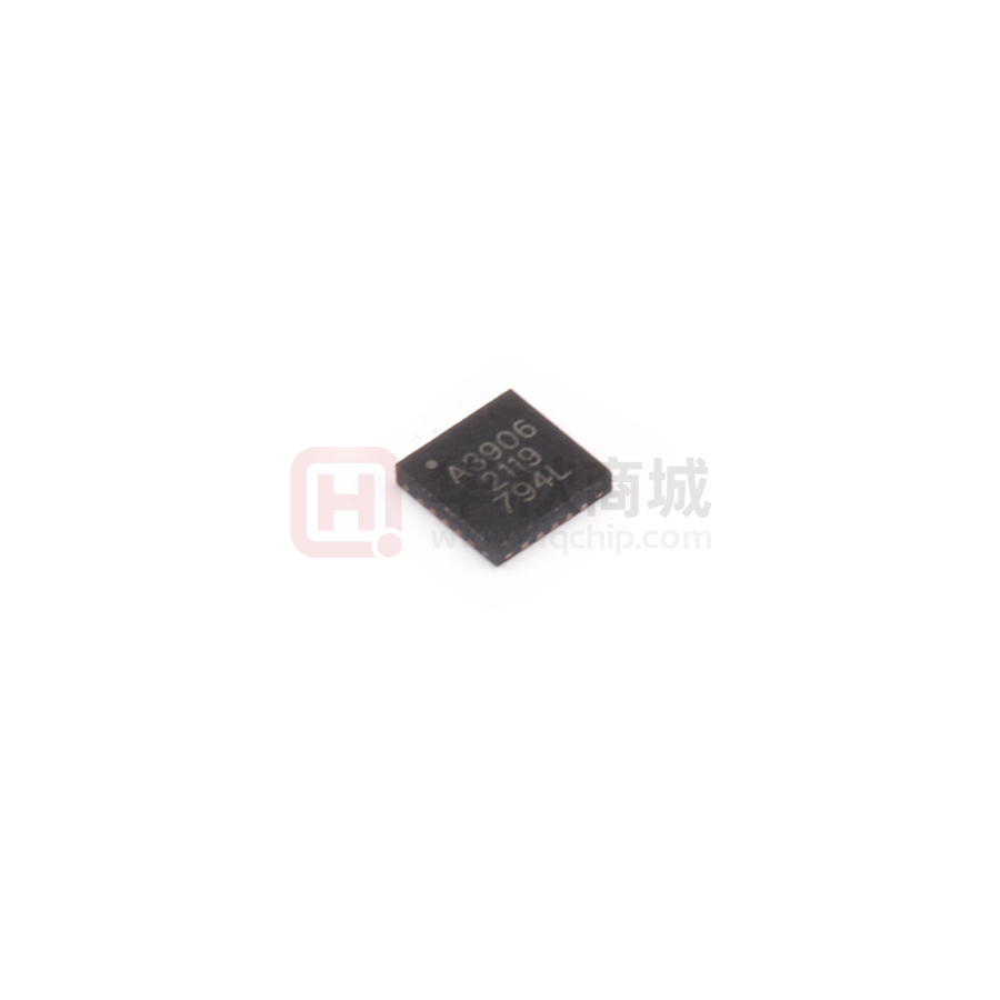
A3906
Low Voltage Stepper and Single/Dual DC Motor Driver
Features and Benefits
Description
▪ 2.5 to 9 V operation
▪ Internal PWM current limit control
▪ Synchronous rectification for reduced power dissipation
▪ Peak current output flag
▪ Undervoltage lockout
▪ Low RDS(on) outputs
▪ Small package
▪ Brake mode for DC motors
▪ Sleep function
▪ Crossover-current protection
▪ Thermal shutdown
Designed for pulse width modulated (PWM) control of low
voltage stepper motors, and single and dual DC motors, the
A3906 is capable of output currents up to 1 A per channel and
operating voltages from 2.5 to 9 V.
The A3906 has an internal fixed off-time PWM timer that
sets a peak current based on the selection of a current sense
resistor. An overcurrent output flag is provided that notifies
the user when the current in the motor winding reaches the
peak current determined by the sense resistor. The fault output
does not affect driver operation.
The A3906 is provided in a 20-contact, 4 mm × 4 mm, 0.75 mm
nominal overall height QFN, with exposed pad for enhanced
thermal dissipation. It is lead (Pb) free, with 100% matte tin
leadframe plating.
Package: 20-contact QFN (suffix ES)
Applications include the following:
▪ Digital still cameras (DSC)
▪ Cell phone cameras
▪ USB powered devices
▪ Battery powered devices
Approximate size
Typical Applications
0.1 μF
0.1 μF
CP1
CP2
CP3
CP4
CP1
VCP
0.1 μF
0.1 μF
CP2
CP4
CP3
VCP
0.1 μF
SLEEP
A3906
A3906
IN2
M
OUT1B
IN4
+5 V
SENSE1
VBB
10 μF
10 V
IN1
OUT1A
IN3
+5 V
SLEEP
10 μF
10 V
IN1
IN2
0.1 μF
VBB
OUT1A
IN3
OUT1B
IN4
SENSE1
M
OUT2A
M
FL1
OUT2B
FL2
GND
SENSE2
Dual DC motor application
3906-DS, Rev. 4
OUT2A
FL1
OUT2B
FL2
SENSE2
GND
Stepper motor application
�A3906
Low Voltage Stepper and Single/Dual DC Motor Driver
Selection Guide
Part Number
Packing
A3906SESTR-T
Package
1500 pieces per 7-in. reel
20-pin QFN with exposed thermal pad
Absolute Maximum Ratings
Characteristic
Symbol
Load Supply Voltage
VBB
Logic Input Voltage Range
VIN
Sense Voltage
VSENSEx
Output Current
IOUT
Output Current in Paralleled
Operation
IOUT(par)
Operating Temperature Range
TA
Junction Temperature
Notes
Continuous
Pulsed, tw < 1 μs
May be limited by duty cycle, ambient
temperature, and heat sinking. Under
any set of conditions, do not exceed
the specified current rating or a junction
temperature of 150°C.
Continuous
Peak, DC < 30%
Continuous
Peak, DC < 30%
Range S
Rating
Units
9.6
V
–0.3 to 7
V
0.5
V
1
V
1
A
1.5
A
2
A
2.5
A
–20 to 85
°C
TJ(max)
150
°C
Tstg
–40 to 150
°C
Storage Temperature Range
Thermal Characteristics may require derating at maximum conditions, see application information
Characteristic
Symbol
RθJA
Package Thermal Resistance
Test Conditions*
Value Units
4-layer PCB based on JEDEC standard
37
ºC/W
*Additional thermal information available on the Allegro website.
Terminal List Table
16 OUT1A
17 VCP
18 CP3
19 CP1
20 CP4
Pin-out Diagram
CP2
1
15
SENSE1
GND
2
14
OUT1B
SLEEP
3
13
VBB
IN1
4
12
OUT2B
IN2
5
11
SENSE2
7
8
9
IN4
FL1
FL2
OUT2A 10
6
IN3
PAD
Number
1
2
3
4
5
Name
CP2
GND
SLEEP
IN1
IN2
6
7
8
9
10
11
12
13
14
15
16
17
18
19
20
–
IN3
IN4
FL1
FL2
OUT2A
SENSE2
OUT2B
VBB
OUT1B
SENSE1
OUT1A
VCP
CP3
CP1
CP4
PAD
Function
Charge pump capacitor terminal 2
Ground
Sleep logic input, active low
Control input
Control input
Control input
Control input
Current limit flag, bridge 1
Current limit flag bridge 2
DMOS full-bridge 2, output A
Current sense resistor terminal, bridge 2
DMOS full-bridge 2, output B
Supply Voltage
DMOS full-bridge 1, output B
Current sense resistor terminal, bridge 1
DMOS full-bridge 1, output A
Reservoir capacitor terminal
Charge pump capacitor terminal 3
Charge pump capacitor terminal 1
Charge pump capacitor terminal 4
Exposed pad for enhanced thermal performance
Allegro MicroSystems, LLC
115 Northeast Cutoff
Worcester, Massachusetts 01615-0036 U.S.A.
1.508.853.5000; www.allegromicro.com
2
�A3906
Low Voltage Stepper and Single/Dual DC Motor Driver
Functional Block Diagram
0.1 μF
0.1 μF
10 μF
10 V
CP4
CP3
CP2
CP1
VCP
0.1 μF
VBB
VCP
Charge Pump
VBB
GND
Regulator
+5 V +5 V
OUT1A
Sense1
Sense2
OUT1B
SLEEP
Sense1
SENSE1
FL1
FL2
PWM Latch and
Blanking
Comparator
Bridge 2
VBB
IN1
IN2
RS1
VCP
PWM Latch and
Blanking
Comparator
Bridge 1
OUT2A
OUT2B
Control Logic
IN3
IN4
Sense2
SENSE2
RS2
Allegro MicroSystems, LLC
115 Northeast Cutoff
Worcester, Massachusetts 01615-0036 U.S.A.
1.508.853.5000; www.allegromicro.com
3
�A3906
Low Voltage Stepper and Single/Dual DC Motor Driver
ELECTRICAL CHARACTERISTICS1,2 valid at TA = 25°C and VBB = 2.5 to 9 V, unless otherwise noted
Characteristics
Symbol
Operating Voltage Range
VBB
VBB Supply Current
IBB
Output Resistance
RDS(on)
Current Trip Sense Voltage
VSENSE
Test Conditions
Output Leakage Current
Vf
IDSS
Typ.
Max.
Units
2.5
–
9
V
IOUT = 0 mA, PWM = 50 kHz, Duty Cycle = 50%
–
5
–
mA
IOUT = 0 mA, outputs disabled, VBB = 9.6 V
–
3
–
mA
Sleep mode, VIN < 0.4 V
–
150
500
nA
Source driver, IOUT = 400 mA , VBB = 3 V, TJ = 25°C
–
0.52
0.60
Ω
Source driver, IOUT = 400 mA , VBB = 3 V, TJ = 85°C
–
0.78
–
Ω
Sink driver, IOUT = 400 mA, VBB = 3 V, TJ= 25°C
–
0.62
0.74
Ω
Sink driver, IOUT = 400 mA, VBB = 3 V, TJ= 85°C
Clamp Diode Voltage
Min.
FLx falling edge
I = 400 mA
Outputs, VOUT = 9 V
–
0.93
–
Ω
160
200
240
mV
–
–
1
V
–20
–
20
μA
Control Logic
Logic Input Voltage
Logic Input Current
Input Hysteresis
¯S¯¯L¯¯E¯¯E¯¯P¯ Input
VIN(1)
2.0
–
5.5
V
VIN(0)
–
–
0.8
V
IIN(1)
VIN = 5.5 V
–
