A3908 Low Voltage DC Motor Driver
Features and Benefits
▪ ▪ ▪ ▪ ▪ ▪ ▪ ▪ Constant voltage operation (adjustable) 500 mA output peak rating Low power standby mode Small 2 mm × 2 mm, 0.55 mm nominal height DFN package Typical input voltage range of 3 to 5.5 V Adjustable constant voltage or PWM operation Less than 500 nA standby mode current –40 to 85 operating temperature range
Description
The A3908 is a low voltage bidirectional DC motor driver with a typical input voltage range of 3 to 5.5 V and output currents up to 500 mA. The unique output full-bridge incorporates sourceside linear operation to allow a constant voltage across the motor coil. This regulated output minimizes motor voltage change due to I × RDS(on) variation and battery voltage tolerance. Logic input pins are provided to control the motor direction of rotation, brake, and standby (< 500 nA supply current) modes and to allow optional PWM of the sink drivers. Internal protection circuitry includes thermal shutdown, undervoltage lockout, and crossover current (shoot-through) protection. The A3908 is supplied in a 2 mm x 2 mm, 0.55 mm nominal height, 8-lead DFN package, with exposed thermal pad (package suffix EE). This small footprint package is lead (Pb) free, with 100% matte tin leadframe plating. Applications include: ▪ ▪ ▪ ▪ ▪ Robotic actuators and pumps Portable printers/scanners Camera lens/shutter control Battery powered toys and games Low noise test instrumentation systems
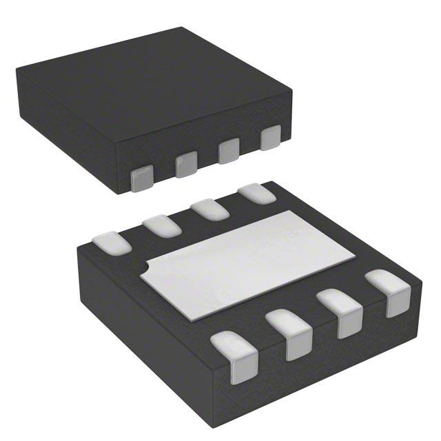
Package: 8 Contact DFN (suffix EE)
Approximate Scale 1:1
Typical Application
+VBAT VDD
IN1 IN2 CPU VREF R1 18 kΩ R2 10 kΩ VSET GND OUTA
A3908
OUTB
M
3908-DS
�A3908
Low Voltage DC Motor Driver
Selection Guide
Part Number A3908EEETR-T Packing Tape and reel, 3000 pieces/reel
Absolute Maximum Ratings
Parameter Supply Voltage Logic Input Voltage Range Output Current Junction Temperature Storage Temperature Range Operating Temperature Range Symbol VDD VIN IOUT TJ Tstg TA Range E – –40 –40 – – – Conditions Min. – –0.3 Typ. – – Max. Units 6 6 500 150 150 85 V V mA °C °C °C
Allegro MicroSystems, Inc. 115 Northeast Cutoff Worcester, Massachusetts 01615-0036 U.S.A. 1.508.853.5000; www.allegromicro.com
2
�A3908
Low Voltage DC Motor Driver
Functional Block Diagram
VDD VREF R1 VSET R2 3R R
OUTA OUTB
3 to 5.5V 10 F
VBG
CHARGE PUMP VCP VSET 3R OUTA R OUTB Sink Drive Sink Drive GND
IN1
IN2
Control Logic
Terminal Diagram
OUTB 1 GND 2 VDD 3 OUTA 4 8 7 6 5 IN2 IN1 VREF VSET
(Top View)
Number 1 2 3 4 5 6 7 8
Name OUTB GND VDD OUTA VSET VREF IN1 IN2
Description Motor terminal Ground Input supply Motor terminal Select source-side output voltage Bandgap reference Control logic input Control logic input
Allegro MicroSystems, Inc. 115 Northeast Cutoff Worcester, Massachusetts 01615-0036 U.S.A. 1.508.853.5000; www.allegromicro.com
3
�A3908
Low Voltage DC Motor Driver
ELECTRICAL CHARACTERISTICS at TA =25°C, and VDD = 3 to 5.5 V, unless otherwise noted Characteristics Symbol Test Conditions Min.
Supply Current UVLO Enable Threshold UVLO Hysteresis Thermal Shutdown Temperature Thermal Shutdown Hysteresis Logic Input Low Level Logic Input High Level Input Hysteresis Logic Input Current Output Driver Sink Driver Output Resistance Source Driver On Resistance Bandgap Reference VOUT Accuracy (VOUTA –VOUTB) RDS RDS(on) VBG VSET = 1.2 V VOUT VSET = 825 mV VSET = 500 mV VDD = 5 V, IOUT = 500 mA VDD = 3 V, IOUT = 500 mA VDD = 5 V, IOUT = 500 mA VDD = 3 V, IOUT = 500 mA – – – – 1.235 4.608 3.135 1.84 IDD IDDSTB VDDUVLO VUVHYS TJTSD TJHYS VIL VIH VHYS IIN VIN = 0 to 5 V Temperature increasing. Recovery = TJTSD – TJHYS Standby mode VDD rising – – – – – – – VDD x 55% – –1
Typ.
0.5 – – 120 165 15 – – VDD x 7% 0 0.6 0.8 0.6 0.65 1.285 4.8 3.3 2
Max.
2 500 2.6 – – – VDD x 20% – – 1 – – – – 1.335 4.992 3.465 2.16
Units
mA nA V mV °C °C V V mV μA Ω Ω Ω Ω V V V V
THERMAL CHARACTERISTICS Characteristics Package Thermal Resistance*
*Additional
Symbol RθJA
Test Conditions Measured on 4-layer board based on JEDEC standard
Rating 49
Unit °C/W
thermal information is available on the Allegro Web site.
Allegro MicroSystems, Inc. 115 Northeast Cutoff Worcester, Massachusetts 01615-0036 U.S.A. 1.508.853.5000; www.allegromicro.com
4
�A3908
Low Voltage DC Motor Driver
Functional Description
Voltage Regulation The A3908 regulates the voltage
Dropout Mode The source and sink drivers have a
across the motor coil. The voltage across the OUTA and OUTB terminal is sensed and compared to an internal threshold voltage. The high-side switch will be driven in linear mode to keep the applied voltage maintained at the calculated level, as follows: VOUT = 4 × VREF (R2 / [R1+R2]) , where VREF (VBG) is 1.285 V typical. Then, for forward mode: VOUT = VOUTA – VOUTB , and for reverse mode: VOUT = VOUTB – VOUTA . The alternative method is to provide a tightly regulated voltage to the motor supply pin and run the source and sink drivers as switches. The voltage drop across these switches will vary linearly with temperature and current, therefore the voltage across the motor coil also will vary. The A3908 will eliminate these sources of error for a system where controlling the motor voltage is the optimum means of control.
Thermal Shutdown The A3908 will disable the out-
total RDS(on) of approximately 1.2 Ω total. When the motor supply voltage, VDD, drops too low compared to the regulated value, the IC enters dropout mode. In this case, the voltage across the motor coil will be: VMOTOR = VDD – ILOAD (RDS(sink) + RDS(src))
Brake Mode When both inputs are high, the A3908
goes into high-side brake mode (turns on both source drivers). There is no protection during braking, so care must be taken to ensure that the peak current does not exceed the absolute maximum current, IOUT.
Standby Mode To minimize battery drain, standby
mode will turn off all of the circuitry and draw typically less than 100 nA from the VDD line. There will be a very short delay, approximately 2 μs, before enabling the output drivers after release of standby mode.
Power Dissipation. Power can be approximated
based on the below three components: PD(src) = ILOAD (VDD –VREG) , PD(sink) = ILOAD × RDS(sink) , and Pbias = VDD × IDD.
puts if the junction temperature, TJ , reaches 165°C. There is 15°C of hysteresis, so when the junction temperature drops below 150°C, the device will begin to operate normally.
Control Logic Table
Settings IN1 0 0 1 1 IN2 0 1 0 1 OUTA Off Low VREG High OUTB Off VREG Low High Resulting Mode Standby Reverse Forward Brake
Allegro MicroSystems, Inc. 115 Northeast Cutoff Worcester, Massachusetts 01615-0036 U.S.A. 1.508.853.5000; www.allegromicro.com
5
�A3908
Low Voltage DC Motor Driver
Application Information
Layout
The printed circuit board should use a heavy groundplane for optimum thermal performance. The A3908 must be soldered directly onto the board. On the underside of the A3908 package is an exposed pad, which provides a path for enhanced thermal dissipation. The thermal pad should be soldered directly to an exposed surface on the PCB. Thermal vias are used to transfer heat to other layers of the PCB. Thermal vias should not have any thermal relief and should be con-
nected to internal layers, if available, to maximize the dissipation area.
Grounding In order to minimize the effects of ground
bounce and offset issues, it is important to have a low impedance, single-point ground, known as a star ground, located very close to the device. By making the connection between the exposed thermal pad and the groundplane directly under the A3908, that area becomes an ideal location for a star ground point. A low impedance ground will prevent ground bounce
OUTB GND VDD OUTA CVDD
GND U1 IN2 IN1 R2 R1
CVDD 10 F
OUTB GND VDD OUTA IN2
A3908
PAD
IN1 VREF
GND
R1
VSET
R2
A3908 Evaluation Board
Allegro MicroSystems, Inc. 115 Northeast Cutoff Worcester, Massachusetts 01615-0036 U.S.A. 1.508.853.5000; www.allegromicro.com
6
�A3908
Low Voltage DC Motor Driver
during PWM operation and ensure that the supply voltage remains stable at the input terminal. Bulk capacitance is often located at a non-ideal distance from the device. If the recommended capacitance of 10 μF cannot be located very close to the supply terminal on the A3908, it is recommended that a 0.1 μF capacitor be placed as close to the VDD terminal as possible to provide a path for transient currents.
PWM Operation
is then controlled using enable chopping, described below.
Enable Chopping By PWMing the logic inputs
In some applications current control may be desired. Pulse width modulating the inputs will allow the output current to be regulated. When external PWM control is used, the VREF pin should be connected directly to the VSET pin. This effectively disables voltage control on the source driver, and allows maximum current to flow through the driver. Current
between enable and brake modes, the current in the motor winding can be controlled. It is accomplished by holding one input high while PWMing the other input. During the on-cycle, current flows in the bridge consistent with the direction programmed on the input pins. During the off-cycle, the A3908 enters brake mode. Enable chopping is illustrated in figure 1. Current in the motor winding is controlled by changing the duty cycle on the PWM input. As shown in figure 2, the average current is still positive but, because the duty cycle is less, the average current is much lower.
IOUT
C3
IOUT
C3
VIN1
VIN1 VIN2
C1 C2 t
VIN2
C1 C2 t
Symbol C1 C2 C3 t
Parameter VIN1 VIN2 IOUT time
Units/Division 2V 2V 100 mA 20 μs
Symbol C1 C2 C3 t
Parameter VIN1 VIN2 IOUT time
Units/Division 2V 2V 100 mA 20 μs
Figure 1. Enable chopping. Forward direction, output duty cycle 90%.
Figure 2. Enable chopping. Forward direction, output duty cycle 20%.
Allegro MicroSystems, Inc. 115 Northeast Cutoff Worcester, Massachusetts 01615-0036 U.S.A. 1.508.853.5000; www.allegromicro.com
7
�A3908
Low Voltage DC Motor Driver
Package EE, 8-contact DFN
0.30 2.00 ±0.15 8 0.83 8 0.50
2.00 ±0.15 A 1 2 1 1.60
0.90
2.13
9X
D 0.08 C 0.25 ±0.05 0.50
SEATING PLANE +0.05 0.55 –0.04
C C
PCB Layout Reference View
1
2
0.325 ±0.050 0.90 B
All dimensions nominal, not for tooling use (reference JEDEC MO-229UCCD) Dimensions in millimeters Exact case and lead configuration at supplier discretion within limits shown A Terminal #1 mark area B Exposed thermal pad (reference only, terminal #1 identifier appearance at supplier discretion) C Reference land pattern layout (reference IPC7351 SON50P200X200X100-9M); All pads a minimum of 0.20 mm from all adjacent pads; adjust as necessary to meet application process requirements and PCB layout tolerances; when mounting on a multilayer PCB, thermal vias at the exposed thermal pad land can improve thermal dissipation (reference EIA/JEDEC Standard JESD51-5) D Coplanarity includes exposed thermal pad and terminals
8
1.60
Copyright ©2008, Allegro MicroSystems, Inc. The products described here are manufactured under one or more U.S. patents or U.S. patents pending. Allegro MicroSystems, Inc. reserves the right to make, from time to time, such departures from the detail specifications as may be required to permit improvements in the performance, reliability, or manufacturability of its products. Before placing an order, the user is cautioned to verify that the information being relied upon is current. Allegro’s products are not to be used in life support devices or systems, if a failure of an Allegro product can reasonably be expected to cause the failure of that life support device or system, or to affect the safety or effectiveness of that device or system. The information included herein is believed to be accurate and reliable. However, Allegro MicroSystems, Inc. assumes no responsibility for its use; nor for any infringement of patents or other rights of third parties which may result from its use. For the latest version of this document, visit our website: www.allegromicro.com
Allegro MicroSystems, Inc. 115 Northeast Cutoff Worcester, Massachusetts 01615-0036 U.S.A. 1.508.853.5000; www.allegromicro.com
8
�