A3935
3-Phase Power MOSFET Controller for Automotive Applications
Features and Benefits
Description
▪
▪
▪
▪
▪
▪
▪
▪
The A3935 is designed specifically for automotive applications
that require high-power motors. Each provides six high-current
gate drive outputs capable of driving a wide range of N-channel
power MOSFETs.
Drives wide range of N-channel MOSFETs in 3-phase bridges
PFM boost converter for use with low-voltage battery supplies
Internal LDO regulator for gate-driver supply
Bootstrap circuits for high-side gate drivers
Current monitor output
Adjustable battery overvoltage detection
Diagnostic outputs
Motor lead short-to-battery, short-to-ground, and bridgeopen protection
▪ Undervoltage protection
▪ –40°C to 150°C TJ operation
▪ Thermal shutdown
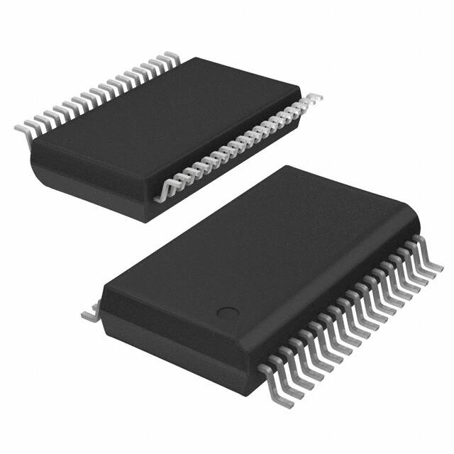
Package 36-pin QSOP (LQ):
Approximate scale 1:1
A requirement of automotive systems is steady operation over
a varying battery input range. The A3935 integrates a pulsefrequency modulated boost converter to create a constant
supply voltage for driving the external MOSFETs. Bootstrap
capacitors are utilized to provide the above battery supply
voltage required for N-channel FETs.
Direct control of each gate output is possible via six TTLcompatible inputs. A differential amplifier is integrated to
allow accurate measurement of the current in the three-phase
bridge.
Diagnostic outputs can be continuously monitored to protect
the driver from short-to-battery, short-to-supply, bridge-open,
and battery under/overvoltage conditions. Additional protection
features include dead-time, VDD undervoltage, and thermal
shutdown.
The A3935 is supplied in a 36-lead 0.8 mm pitch QSOP (package
LQ, similar to SOICW). The lead (Pb) free variants (suffix –T )
have 100% matte tin leadframe plating.
Typical Application
26301.102J
�A3935
3-Phase Power MOSFET Controller for Automotive Applications
Selection Guide
Part Number
Pb-free
A3935KLQTR1
A3935KLQTR-T2
1Variant
–
Yes
Packing
Terminals
1500 pieces/reel
Package
QSOP (similar to
SOICW) surface mount
36
has been determined to be obsolete and is no longer in production. Status change: October 31, 2011.
2Variant
is in production but has been determined to be NOT FOR NEW DESIGN. This classification indicates that
sale of the variant is currently restricted to existing customer applications. The variant should not be purchased for
new design applications because obsolescence in the near future is probable. Samples are no longer available.
Status change: October 31, 2011.
Absolute Maximum Ratings
Parameter
Symbol
VBAT
Load Supply Voltage
VDRAIN
VDRAIN pin
VBOOST
VBOOST pin
VBOOSTD
VBOOSTD pin
VGHx
Output Voltage Range
Sense Circuit Voltage
Logic Supply Voltage
Logic Input/Output
Conditions
Rating
Units
–0.6 to 40
V
–4 to 55
V
VBAT pin
GHA, GHB, and GHC pins
VSx
SA, SB, and SC pins
–4 to 40
V
VGLx
GLA, GLB, and GLC pins
–4 to 16
V
–0.6 to 55
V
–4 to 6.5
V
–0.3 to 6.5
V
VCx
CA, CB, and CC pins
VCSx
CSN and CSP pins
VLSS
LSS pin
VDD
VDD pin
VOVSET
OVSET pin
VBOOSTS
BOOSTS pin
VCSOUT
CSOUT pin
VDSTH
VDSTH pin
remaining logic pins
ESD Rating – Human Body Model
AEC-Q100-002; all pins
2.5
kV
ESD Rating – Charged Device Model
AEC-Q100-011; all pins
1050
V
–40 to 135
°C
150
°C
–55 to 150
°C
Operating Temperature
Junction Temperature*
Storage Temperature Range
TA
TJ(max)
Tstg
Range K
Fault conditions that produce excessive junction temperature
will activate device thermal shutdown circuitry. These conditions can be tolerated, but should be avoided.
Allegro MicroSystems, Inc.
115 Northeast Cutoff, Box 15036
Worcester, Massachusetts 01615-0036 (508) 853-5000
www.allegromicro.com
2
�A3935
3-Phase Power MOSFET Controller for Automotive Applications
Functional Block Diagram
BOOSTD
VBAT
VBOOST
BOOSTS
VDRAIN
(KELVIN)
Low Drop
Out
Linear
Regulator
OS
(off)
VREG
VBAT
VIGN
Motor
Supply
Voltage
REFi
REFv
Phase A
OS
(blank)
External +5V
VDD
CA
CBOOT
AHI
Turn ON
Delay
High-Side
Driver
To P hase C
GHA
ALO
BHI
BLO
Control
Logic
SA
CHI
VREG
CLO
ENABLE
Turn ON
Delay
Low-Side
Driver
GLA
To P hase B
FAULT
OVFLT
LSS
VBAT Overvoltage
VBAT Undervoltage
UVFLT
VBAT
OVSET
SA
SB
VREG Undervoltage
Short to Ground
Short to Battery
Bridge Open
cs
RS
VDD
CSN
VDD Undervoltage
Thermal Shutdown
GND
SC
VDSTH
CSP
VREG
Drain-Source
Fault Monitor
LSS
VDD
VDRAIN
CSOUT
Dwg. FP-053
Allegro MicroSystems, Inc.
115 Northeast Cutoff, Box 15036
Worcester, Massachusetts 01615-0036 (508) 853-5000
www.allegromicro.com
3
�A3935
3-Phase Power MOSFET Controller for Automotive Applications
ELECTRICAL CHARACTERISTICS at TJ = –40°C to 150°C, VBAT = 7 to 16 V, VDD = 4.75 to 5.25 V, ENABLE = 22.5 kHz,
50% duty cycle, two phases active;unless otherwise noted
Characteristics
Power Supply
VDD Supply Current
VBAT Supply Current
Battery Voltage Operating Range
Symbol
Bootstrap Diode Forward Voltage
VDBOOT
Bootstrap Diode Resistance
rDBOOT
Bootstrap Diode Current Limit2
Bootstrap Quiescent Current
Bootstrap Refresh Time
VREG Output Voltage3
VREG Dropout Voltage4
Gate Drive Average Supply Current
VREG Input Bias Current
Boost Supply
VBOOST Output Voltage Limit
VBOOST Output Voltage Limit Hysteresis
Boost Switch On Resistance
Boost Switch Maximum Current
Boost Current Limit Threshold Voltage
Off Time
Blanking Time
Control Logic
IDD
IBAT
VBAT
IDM
ICx
trefresh
VREG
VREGDO
IREG
IREGbias
Conditions
All logic inputs = 0 V
All logic inputs = 0 V
IDBOOT = –ICx = 10 mA, VDBOOT = VREG – VCx
IDBOOT = –ICx = 100 mA
rDBOOT(100 mA) = (VDBOOT(150 mA)
– VDBOOT(50 mA)) / 100 mA
3 V < VREG – VCx < 12 V
VCx = 40 V, GHx = ON
VSx = low, to guarantee ΔV = +0.5 V refresh of 0.47 μF
Bootstrap Capacitor, CBOOT, to VCx – VSx = +10 V
VBAT = 7 to 40 V, VBOOST from Boost Regulator
VREGDO = VBOOST – VREG, IREG = 40 mA
No external dc load at VREG, CREG = 10 μF
Current into VBOOST, ENABLE = 0
VBOOSTM VBAT = 7 V
∆VBOOSTM
rDS(on)
IBOOSTD < 300 mA
IBOOSTSW
VBI(th)
Increasing VBOOSTS
toff
tblank
Minimum high level input for logic 1
Maximum low level input for logic 0
VI = VDD
VI = 0.8 V
Logic Input Hysteresis
VI(1)
VI(0)
II(1)
II(0)
VIhys
Logic Output High Voltage
VO(H)
IO(H) = –800 μA
Logic Input Voltage
Logic Input Current
Logic Output Low Voltage
VO(L)
IO(L) = 1.6 mA
Gate Drives, GHx (internal source, or upper, switch stages)5
GHx: IxU = –10 mA, VSx = 0
Output High Voltage
VDSL(H)
GLx: IxU = –10 mA, VLSS = 0
Source Current (pulsed)
Source On Resistance
IxU
rSDU(on)
VSDU = 10 V, TJ = 25°C
VSDU = 10 V, TJ = 135°C
IxU = –150 mA, TJ = 25°C
IxU = –150 mA, TJ = 135°C
Min.
Typ1.
Max.
Units
–
–
7.0
0.8
1.5
–
–
–
–
–
7.0
3.0
40
2.0
2.3
mA
mA
V
V
V
2.5
–
7.5
Ω
–150
10
–
–
–1150
30
mA
μA
–
–
2.0
μs
12.7
–
–
–
–
0.9
–
–
14
–
40
4.0
V
V
mA
mA
14.9
35
–
–
0.45
3.0
100
–
–
1.4
–
–
–
–
16.3
180
3.3
300
0.55
8.0
220
V
mV
Ω
mA
V
μs
ns
2.0
–
–
50
100
VDD –
0.8
–
–
–
–
–
–
–
0.8
500
–
300
V
V
μA
μA
mV
–
–
V
–
0.4
V
–
VREG
V
–
VREG
V
800
–
–
–
–
–
10
15
mA
mA
Ω
Ω
VREG –
2.26
VREG –
0.26
–
400
4.0
7.0
Continued on the next page…
Allegro MicroSystems, Inc.
115 Northeast Cutoff, Box 15036
Worcester, Massachusetts 01615-0036 (508) 853-5000
www.allegromicro.com
4
�A3935
3-Phase Power MOSFET Controller for Automotive Applications
ELECTRICAL CHARACTERISTICS (continued) at TJ = –40°C to 150°C, VBAT = 7 to 16 V, VDD = 4.75 to 5.25 V,
ENABLE = 22.5 kHz, 50% duty cycle, two phases active;unless otherwise noted
Min.
Typ1.
Max.
Units
VDSL = 10 V, TJ = 25°C
VDSL = 10 V, TJ = 135°C
IxL = 150 mA, TJ = 25°C
IxL = 150 mA, TJ = 135°C
–
550
1.8
3.0
850
–
–
–
–
–
6.0
7.5
mA
mA
Ω
Ω
tpd
tsk(o)
tdead
Logic input to unloaded GHx, GLx
Grouped by edge, phase–to–phase
Between GHx, GLx transitions of same phase
–
–
75
–
–
–
150
50
180
ns
ns
ns
Ibias
IIO
CSP = CSN = 0 V
CSP = CSN = 0 V
CSP with respect to GND
CSN with respect to GND
VID = CSP – CSN, –1.3V < CSP,N < 4V
CSP = CSN = 0 V
CSP = CSN = 0 V
CSP = CSN
VID = 40 to 200 mV
VID = 0 to 40 mV, VO = (19.2 × VID) + VO + Ev
CSP = CSN = 200 mV
VCSOUT = 2.0 V
–180
–
–
–
–
77
–
–1.5
18.6
–
28
–
–
–
80
4.0
–
250
100
–
19.2
–
–
8.0
μA
μA
kΩ
kΩ
mV
mV
μV/°C
V
V/V
mV
dB
Ω
ICSOUT = –100 μA at top rail, 100 μA at bottom rail
0.075
–
VCSOUT = 2.5 V
VCSOUT = 2.5 V
CSP = CSN = GND, frequency = 0 to 1 MHz
CSP = CSN = GND, frequency = 0 to 300 kHz
10 mV input
Vcm = 250 mV(pp), frequency = 0 to 800 kHz
200 mV step input, measured at 10/90% points
20
–1.0
20
45
–
26
10
–
–
–
–
1.6
–
–
–360
±35
–
–
±200
450
–
4.0
19.8
±25
–
–
VDD –
0.25
–
–
–
–
–
–
–
3.8
100
0
0
–1.0
19.4
19.4
9.0
–
–
–
–
–
–
22.4
–
4.3
300
VDD
2.5
1.0
40
25.4
15
V
mV
V
V
μA
V
V
%
Characteristics
Symbol
Gate Drives, GLx (internal sink or lower switch stages)6
Sink Current (pulsed)
Sink On Resistance
Gate Drives, GHx, GLx (General)5,6
Propagation Delay, Logic only
Output Skew Time
Dead Time (shoot–through prevention)
Sense Amplifier
Input Bias Current2
Input Offset Current2
Input Resistance
Diff. Input Operating Voltage
Output Offset Voltage
Output Offset Voltage Drift
Input Common Mode Operating Range
Voltage Gain
Low Output Voltage Error
DC Common Mode Attenuation
Output Resistance
Output Dynamic Range
Output Current, Sink
Output Current, Source2
VDD Supply Ripple Rejection
VREG Supply Ripple Rejection
Small Signal 3 dB Bandwidth
AC Common Mode Attenuation
Output Slew Rate (positive or negative)
Fault Logic
VDD Undervoltage
VDD Undervoltage Hysteresis
OVSET Operating Voltage Range
OVSET Calibrated Voltage Range
OVSET Input Current Range2
VBAT Overvoltage Range
VBAT Overvoltage Hysteresis
IxL
rDSL(on)
ri
VID
VOO
ΔVOO
VIC
AV
EV
A VC
rO
VCSOUT
Isink
Isource
PSRRVDD
PSRRVREG
BWf3db
A VC(ac)
SR
Conditions
VDD(uv) Decreasing VDD
∆VDD(uv) VDD(recovery) – VDD(uv)
VSET(ov)
VSET(ov)cal
ISET(ov)
0 V < VSET(ov) < 2.5 V
VBAT(ov)
Increasing VBAT, VSET(ov) = 0 V
∆VBAT(ov) Percent of VBAT(ov) value set by VSET(ov)
V
mA
mA
dB
dB
MHz
dB
V/μs
Continued on the next page…
Allegro MicroSystems, Inc.
115 Northeast Cutoff, Box 15036
Worcester, Massachusetts 01615-0036 (508) 853-5000
www.allegromicro.com
5
�A3935
3-Phase Power MOSFET Controller for Automotive Applications
ELECTRICAL CHARACTERISTICS (continued) at TJ = –40°C to 150°C, VBAT = 7 to 16 V, VDD = 4.75 to 5.25 V,
ENABLE = 22.5 kHz, 50% duty cycle, two phases active;unless otherwise noted
Characteristics
Symbol
VBAT Overvoltage Gain Constant
KBAT(ov)
VBAT Undervoltage
VBAT Undervoltage Hysteresis
VREG Undervoltage
VDSTH Input Range
VDSTH Input Current
VBAT(uv)
VBAT(uv)
VREG(uv)
VDSTH
IDSTH
Conditions
VBAT(ov) = (KBAT(ov) x VSET(ov)) + VBAT(ov)(0);
VBAT(ov)(0) at VSET(ov) = 0
Decreasing VBAT
Percent of VBAT(uv)
Decreasing VREG
VDSTH > 0.8 V
With a high–side driver on, as VSX decreases,
VDRAIN – VSx > VSTG causes a fault
With a low–side driver on, as VSX increases,
VSx – VLSS > VSTB causes a fault
Min.
Typ1.
Max.
Units
–
12
–
V/V
5.0
8.0
9.9
0.5
40
5.25
–
–
–
–
5.5
12
11.1
3.0
100
V
%
V
V
μA
VDSTH +
V
0.2
VDSTH +
Short–to–Battery Threshold
VSTB(th)
–
V
0.2
VBAT +
VDRAIN-Open Bridge Operating Range
VDRAIN 7 V < VBAT < 40 V
V
–0.3
–
2.0
VDRAIN-Open Bridge Current
IVDRAIN 7 V < VBAT < 40 V
0
–
1.0
mA
VDRAIN /Open Bridge Threshold Voltage
VBDGO(th) If VDRAIN < VBDGOTH then a bridge fault occurs
1.0
–
3.0
V
160
170
180
°C
Thermal Shut Down Temperature
TJ
Thermal Shutdown Hysteresis
∆TJ
7.0
10
13
°C
1Typical data are for initial design estimations only, and assume optimum manufacturing and application conditions. Performance may vary for individual
units, within the specified maximum and minimum limits.
2Negative current is defined as coming out of (sourcing) the specified device terminal.
3For V
BOOSTM < VBOOST < 40 V power dissipation in the VREG LDO increases. Observe TJ < 150°C limit.
4With V
BOOST decreasing, dropout voltage measured at VREG = VREG(ref) – 200 mV where VREG(ref) = VREG at VBOOST = 16 V.
5For GHx: V
SDU = VCx – VGHx, VDSL = VGHx – VSx, VDSL(H) = VCx – VSDU – VSx.
6For GLx: V
SDU = VREG – VGLx, VDSL = VGLx – VLSS, VDSL(H) = VREG – VSDU – VLSS.
Short–to–Ground Threshold
VSTG(th)
VDSTH –
0.3
VDSTH –
0.3
–
Allegro MicroSystems, Inc.
115 Northeast Cutoff, Box 15036
Worcester, Massachusetts 01615-0036 (508) 853-5000
www.allegromicro.com
6
�A3935
3-Phase Power MOSFET Controller for Automotive Applications
Thermal Characteristics
Characteristic
Package Thermal Resistance
Symbol
RθJA
Test Conditions*
Value Units
On 4-layer PCB, based on JEDEC standard
44
ºC/W
*Additional thermal information available on Allegro Web site.
ALLOWABLE PACKAGE POWER DISSIPATION IN WATTS
Power Dissipation versus Ambient Temperature
5.0
4.0
3.0
2.0
R
θJA
=4
4°C
/W
*
1.0
0
25
50
75
100
125
AMBIENT TEMPERATURE IN °C
150
Allegro MicroSystems, Inc.
115 Northeast Cutoff, Box 15036
Worcester, Massachusetts 01615-0036 (508) 853-5000
www.allegromicro.com
7
�A3935
3-Phase Power MOSFET Controller for Automotive Applications
Terminal Descriptions
AHI, BHI, and CHI. Direct control of high-side gate outputs
GHA, GHB, and GHC. Logic 1 drives the gate on. Logic 0 pulls
the gate down, turning off the external power MOSFET. Internally pulled down when the terminal is open.
ALO, BLO, and CLO. Direct control of low-side gate outputs
GHA, GHB, and GHC. Logic 1 drives the gate on. Logic 0 pulls
the gate down, turning off the external power MOSFET. Internally pulled down when the terminal is open.
BOOSTD. Boost converter switch drain connection.
BOOSTS. Boost converter switch source connection.
CA, CB, and CC. High-side connection for the bootstrap
capacitors, CBOOTx, positive supply for high-side gate drive.
The bootstrap capacitor is charged to VREG when the output Sx
terminal is low. When the output swings high, the voltage on this
terminal rises with the output to provide the boosted gate voltage
needed for N-channel power MOSFETs.
CSN. Input for current-sense differential amplifier, on the
inverting, negative side. Kelvin connection for the ground side of
the current-sense resistor, RSENSE.
CSOUT. Amplifier output voltage proportional to the current
sensed across an external low-value resistor placed in the ground
side of the power MOSFET bridge.
CSP. Input for current-sense differential amplifier, on the noninverting, positive side. Connected to the positive side of the
sense resistor, RSENSE.
ENABLE. Logic 0 disables the gate control signals and switches
off all the gate drivers (low) causing a coast condition. Can be
used in conjunction with the gate inputs to PWM (pulse wave
modulate) the load current. Internally pulled down when the
terminal is open.
¯F
¯¯
A¯¯
U¯¯
L
¯¯
T
¯ . Diagnostic logic output signal. When low, indicates
that one or more fault conditions have occurred.
GHA, GHB, and GHC. High-side gate drive outputs for
N-channel MOSFET drivers. External series gate resistors can
control the slew rate seen at the power driver gate, thereby
controlling the di/dt and dv/dt of Sx outputs.
GLA, GLB, and GLC. Low-side gate drive outputs for external,
N-channel MOSFET drivers. External series gate resistors can
control slew rate.
GND. Ground, or negative, side of VDD and VBAT supplies.
LSS. Low-side gate driver return. Connects to the common
sources on the low sides of the power MOSFET bridge.
OVFLT. Logic 1 indicates that the VBAT level exceeded the
VBAT overvoltage trip point set by the OVSET level. It will
recover after exceeding a hysteresis below that maximum value.
Normally, it has a high-impedance state. If OVFLT and UVFLT
are both in high-impedance state; then, at least, a thermal
shutdown or VDD undervoltage has occurred.
OVSET. A positive dc level that controls the VBAT overvoltage
trip point. Usually, set by a precision resistor divider network
between VDD and GND, but can be held grounded for a preset
value. When this terminal is open, it sets an unspecified but high
overvoltage trip point.
SA, SB, and SC. Directly connected to the motor terminals,
these terminals sense the voltages switched across the load and
are connected to the negative side of the bootstrap capacitors,
CBOOTx. Also, are the negative supply connection for the
floating high-side drivers.
UVFLT. Logic 1 indicates that the VBAT level is below its
minimum value. It will recover after exceeding a hysteresis above
that minimum value. Has a high-impedance state. If UVFLT and
OVFLT are both in high-impedance state; then, at least, a thermal
shutdown or VDD undervoltage has occurred.
VBAT. Battery voltage. Positive input. usually connected to the
motor voltage supply.
VBOOST. Boost converter output, 16 V nominal, is also the
input to the regulator for VREG. Has internal boost-current
and boost-voltage control loops. In high-voltage systems is
approximately one diode drop below VBAT.
VDD. Logic supply, +5 V nominal.
VDRAIN. Kelvin connection for drain-to-source voltage monitor.
Connected to the high-side drains of the MOSFET bridge. High
impedance when this terminal is open, and registers as a short-toground fault on all motor phases.
VDSTH. A positive dc level that sets the drain-to-source monitor
threshold voltage. Internally pulled down when this terminal is
open.
VREG. High-side gate driver supply, 13.5 V nominal. Has lowvoltage dropout (LDO) feature.
Allegro MicroSystems, Inc.
115 Northeast Cutoff, Box 15036
Worcester, Massachusetts 01615-0036 (508) 853-5000
www.allegromicro.com
8
�A3935
3-Phase Power MOSFET Controller for Automotive Applications
Functional Description
Motor Lead Protection. A fault detection circuit monitors
the voltage across the drain-to-source of the external MOSFETs.
A fault is asserted low on the output terminal, F
¯ ¯A¯¯U¯¯L
¯¯T
¯, if the
drain-to-source voltage of any MOSFET that is instructed to
turn on is greater than the voltage applied to the VDSTH input
terminal. When a high-side switch is turned on, the voltage from
VDRAIN to the appropriate motor phase output, VSX, is examined.
If the motor lead is shorted to ground before the high-side is
turned on, the measured voltage will exceed the threshold and
the F
¯ ¯A¯¯U¯¯L
¯¯T
¯ terminal will go low. Similarly, when a low-side
MOSFET is turned on, the differential voltage between the motor
phase (drain) and the LSS terminal (source) is monitored. VDSTH
is set by a resistor divider to VDD.
The VDRAIN is intended to be a Kelvin connection for the
high-side, drain-to-source monitor circuit. Voltage drops across
the power bus are eliminated by connecting an isolated PCB trace
from the VDRAIN terminal to the drain of the MOSFET bridge.
This allows improved accuracy in setting the VDSTH threshold
voltage. The low-side, drain-to-source monitor uses the LSS
terminal, rather than VDRAIN, for comparison with VDSTH.
The A3935 just reports these motor faults.
Fault Outputs. Transient faults on any of the fault outputs
are to be expected during switching, and will not disable the
gate drive outputs. External circuitry or controller logic must
determine if the faults represent a hazardous condition.
¯F¯¯A¯¯U¯¯L¯¯T¯. This terminal will go active low when any of the following conditions occur:
• VBAT overvoltage
• VBAT undervoltage
• Motor lead short-to-supply
or short-to-battery
• Bridge (or VDRAIN) open
• VREG undervoltage
• VDD undervoltage
• Motor lead short-to-ground
• Thermal shut down
OVFLT. Asserts high when a VBAT overvoltage fault occurs and
resets low after a recovery hysteresis. It has a high-impedance
state when a thermal shutdown or VDD undervoltage occurs. The
voltage at the OVSET terminal, VOVSET, controls the VBAT overvoltage set point VBAT(ov), as follows:
VBAT(ov) = (ABAT(ov) × VSET(ov)) + VBAT(ov)(0),
where ABAT(ov) is the gain (12) and VBAT(ov)(0) is the value of
VBAT(ov) when VSET(ov) = 0 (VBAT(ov) ≈ 22.4). For the above
formula to be valid, all variables must be in range and below the
maximum operating specification.
UVFLT. Asserts high when a VBAT undervoltage fault occurs and
resets low after exceeding a recovery hysteresis. It has a highimpedance state when a thermal shut down or VDD undervoltage
occurs. OVFLT and UVFLT are mutually exclusive by definition.
Current Sensing. A current-sense amplifier is provided to
allow system monitoring of the load current. The differential
amplifier inputs are intended to be Kelvin-connected across a
low-value sense resistor or current shunt. The output voltage is
represented by:
VCSOUT = ( ILOAD ×AV × RSENSE) + VOS
where VOS is the output voltage calibrated at zero load current
and A V is the differential amplifier gain of about 19.2. If either
the CSP or CSN pin is open, the CSOUT pin will go to its
maximum positive level.
Shut Down. If a fault occurs because of excessive junction
temperature or undervoltage on VDD or VBAT, all gate driver
outputs are driven low until the fault condition is removed. In
addition, the boost supply switch and VREG are turned off until
those undervoltages and junction temperatures recover.
Boost Supply. VBOOST is controlled by an inner currentcontrol loop, and by an outer voltage-feedback loop. The
current-control loop turns off the boost switch for 5 μs whenever
the voltage across the boost current-sense resistor exceeds
500 mV. A diode reverse-recovery current flows through the
sense resistor whenever the boost switch turns on, which could
result in turning off the switch again if not for the blanking-time
circuit. Adjustment of this external sense resistor determines the
maximum current in the inductor. Whenever VBOOST exceeds the
predefined threshold, 16 V nominal the boost switch is inhibited.
Allegro MicroSystems, Inc.
115 Northeast Cutoff, Box 15036
Worcester, Massachusetts 01615-0036 (508) 853-5000
www.allegromicro.com
9
�A3935
3-Phase Power MOSFET Controller for Automotive Applications
Input Logic Table
Input
Output
Mode of Operation
ENABLE
xLO
xHI
GLx
GHx
0
Don’t Care
Don’t Care
0
0
All gate drive outputs low
1
0
0
0
0
Both gate drive outputs low
1
0
1
0
1
High-side on
1
1
0
1
0
Low-side on
1
1
1
0
0
XOR circuitry prevents shoot-through
Fault Output
Regulator State
Driver Output
UVFLT
Boost
VREG
GHx
GLx
0
ON
ON
a
a
a
Fault Response Table
Operating Conditions
Fault Mode
No Fault
ENABLE
Don’t Care
¯
F
¯¯
A¯¯
U¯¯
L
¯¯
T
¯ OVFLT
1
0
Short-to-Battery
1b
0
0
0
ON
ON
a
Short-to-Ground
1c
0
0
0
ON
ON
a
a
Bridge (VDRAIN) Fault
1d
0
0
0
ON
ON
a
a
VREG Undervoltage
Don’t Care
0
0
0
ON
ON
a
a
VBAT Overvoltage
Don’t Care
0
1
0
OFFe
ON
a
a
VBAT
Undervoltagef
Don’t Care
0
0
1
OFF
OFF
0
0
VDD Undervoltagef
Don’t Care
0
High Z
High Z
OFF
OFF
0
0
Thermal Shut Downf
Don’t Care
0
High Z
High Z
OFF
OFF
0
0
aDetermined
by input states: xLO, xHI, and ENABLE. See Input Logic table.
bShort-to-battery can only be detected when the corresponding GLx = 1. This fault is not detected when ENABLE = 0.
cShort-to-ground can only be detected when the corresponding GHx = 1. This fault is not detected when ENABLE = 0.
dBridge fault appears as a short-to-ground fault on all motor phases. This fault is not detected when ENABLE = 0.
eOff only because V
BOOST ≈ VBAT , which is above the voltage threshold of the Boost regulator voltage control loop.
fThese faults are not only reported, but also action is taken by the internal logic to protect the A3935 and the system.
10
Allegro MicroSystems, Inc.
115 Northeast Cutoff, Box 15036
Worcester, Massachusetts 01615-0036 (508) 853-5000
www.allegromicro.com
�A3935
3-Phase Power MOSFET Controller for Automotive Applications
Pin-out Diagram
CSP
1
36 CSN
VDSTH
2
35 VDD
LSS
3
34 CSOUT1
GLC
4
33 OVSET
SC
5
32 ENABLE
GHC
6
31 CHI
CC
7
30 CLO
GLB
8
29 BLO
SB
9
28 BHI
GHB 10
27 AHI
CB
26 ALO
11
GLA 12
25 FAULT
SA 13
24 OVFLT
GHA 14
23 UVFLT
CA 15
22 VBAT
VREG 16
21 GND
VDRAIN 17
20 BOOSTD
VBOOST 18
19 BOOSTS
Terminal List
Number
Name
1
CSP
2
VDSTH
3
Function
Number
Name
Function
Current-sense input, positive-side
19
BOOSTS
DC input, drain-to-source monitor threshold voltage
20
BOOSTD
LSS
Gate-drive source return, low-side
21
GND
4
GLC
Gate-drive C output, low-side
22
VBAT
Battery supply, positive
5
SC
Load phase C input
23
UVFLT
VBAT undervoltage fault output
6
GHC
Gate-drive C output, high-side
24
OVFLT
VBAT overvoltage fault output
7
CC
Bootstrap capacitor C
25
¯F
¯¯
A
¯¯
U¯¯
L¯¯
T
¯
Active-low fault output, primary
8
GLB
Gate-drive B output, low-side
26
ALO
Gate control input A, low-side
9
SB
Load phase B input
27
AHI
Gate control input A, high-side
10
GHB
Gate-drive B output, high-side
28
BHI
Gate control input B, high-side
11
CB
Bootstrap capacitor B
29
BLO
Gate control input B, low-side
12
GLA
Gate-drive A output, low-side
30
CLO
Gate control input C, low-side
13
SA
Load phase A input
31
CHI
14
GHA
Gate-drive A output, high-side
32
ENABLE
Bootstrap capacitor A
33
OVSET
DC input, overvoltage threshold setting for VBAT
Gate drive supply, positive
34
CSOUT
Current-sense amplifier output
15
CA
16
VREG
Boost switch, source
Boost switch, drain
Ground, dc supply returns, negative
Gate control input C, high-side
Gate output enable
17
VDRAIN
Kelvin connection to MOSFET high-side drains
35
VDD
Logic supply, nominally +5 V
18
VBOOST
Boost supply output
36
CSN
Current-sense input, negative-side
11
Allegro MicroSystems, Inc.
115 Northeast Cutoff, Box 15036
Worcester, Massachusetts 01615-0036 (508) 853-5000
www.allegromicro.com
�A3935
3-Phase Power MOSFET Controller for Automotive Applications
Package LQ, 36-pin QSOP
15.30 ±0.10
0.80
0.60
4° ±4
36
+0.05
0.28 –0.04
2.15
7.50 ±0.10
B
9.50
10.31 ±0.30
A
+0.44
0.84 –0.43
1 2
(0.36)
36X
SEATING
PLANE
0.10 A
+0.12
0.40 –0.11
(0.80)
2.64 MAX
0.20 ±0.10
C
SEATING PLANE
GAGE PLANE
A Terminal #1 mark area
For Reference Only
(QSOP, nonJEDEC standard)
Dimensions in millimeters
Dimensions exclusive of mold flash, gate burrs, and dambar protrusions
Exact case and lead configuration at supplier discretion within limits shown
B Reference land pattern layout (reference IPC7351
SOP80P1033X264-36M); adjust as necessary to meet
application process requirements and PCB layout
tolerances. All pads a minimum of 0.20 mm from all
adjacent pads; adjust as necessary to meet application
process requirements and PCB layout tolerances
12
Allegro MicroSystems, Inc.
115 Northeast Cutoff, Box 15036
Worcester, Massachusetts 01615-0036 (508) 853-5000
www.allegromicro.com
�A3935
3-Phase Power MOSFET Controller for Automotive Applications
Revision History
Revision
Revision Date
Rev. J
October 31, 2011
Description of Revision
Update product availability
Copyright ©2005-2011, Allegro MicroSystems, Inc.
Allegro MicroSystems, Inc. reserves the right to make, from time to time, such departures from the detail specifications as may be required to permit improvements in the performance, reliability, or manufacturability of its products. Before placing an order, the user is cautioned to verify that the
information being relied upon is current.
Allegro’s products are not to be used in life support devices or systems, if a failure of an Allegro product can reasonably be expected to cause the
failure of that life support device or system, or to affect the safety or effectiveness of that device or system.
The information included herein is believed to be accurate and reliable. However, Allegro MicroSystems, Inc. assumes no responsibility for its use;
nor for any infringement of patents or other rights of third parties which may result from its use.
For the latest version of this document, visit our website:
www.allegromicro.com
13
Allegro MicroSystems, Inc.
115 Northeast Cutoff, Box 15036
Worcester, Massachusetts 01615-0036 (508) 853-5000
www.allegromicro.com
�