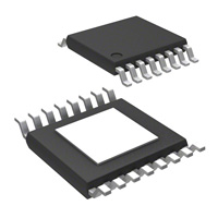
A3946
Half-Bridge Power MOSFET Controller
FEATURES AND BENEFITS
▪ On-chip charge pump for 7 V minimum input
supply voltage
▪ High-current gate drive for driving a wide range of
N‑channel MOSFETs
▪ Bootstrapped gate drive with top-off charge pump
for 100% duty cycle
▪ Overtemperature protection
▪ Undervoltage protection
▪ –40°C to 135°C ambient operation
PACKAGE: 16-pin TSSOP with exposed
thermal pad (Suffix LP)
DESCRIPTION
The A3946 is designed specifically for applications that require
high power unidirectional DC motors, three-phase brushless DC
motors, or other inductive loads. The A3946 provides two
high-current gate drive outputs that are capable of driving a
wide range of power N-channel MOSFETs. The high-side gate
driver switches an N-channel MOSFET that controls current to
the load, while the low-side gate driver switches an N-channel
MOSFET as a synchronous rectifier.
A bootstrap capacitor provides the above-battery supply voltage
required for N-channel MOSFETs. An internal top-off charge
pump for the high side allows DC (100% duty cycle) operation
of the half-bridge.
The A3946 is available in a power package: a 16‑lead TSSOP
with exposed thermal pad (suffix LP). It is lead (Pb) free, with
100% matte tin plated leadframe (suffix -T).
Approximate footprint
Typical Application
VBAT
BOOT
VBB
~FAULT
ECU
IN1
IN2
RESET
DT
DS-A3946, Rev. 10
MCO-0001191
GH
A3946
PAD
S
GL
CP1
M
CP2
VREF
VREG
LGND
PGND
February 18, 2022
�A3946
Half-Bridge Power MOSFET Controller
SELECTION GUIDE
Part Number
Packing
Package
A3946KLPTR-T
4000 pieces/reel
16-pin TSSOP with exposed thermal pad
ABSOLUTE MAXIMUM RATINGS
Rating
Units
Load Supply Voltage
Characteristic
VBB
60
V
Logic Inputs Voltage
VIN
–0.3 to 6.5
V
Pin S Voltage
VS
–4 to 60
V
VGH
–4 to 75
V
VBOOT
–0.6 to 75
V
Pin GH Voltage
Pin BOOT Voltage
Symbol
Notes
Pin DT Voltage
VDT
VREF
V
Pin VREG Voltage
VREG
–0.6 to 15
V
–40 to 135
°C
150
°C
Operating Ambient Temperature
TA
Maximum Junction Temperature
TJ(max)
Storage Temperature
Range K
–55 to 150
°C
ESD Rating, Human Body Model
Tstg
AEC-Q100-002, all pins
2000
V
ESD Rating, Charged Device Model
AEC-Q100-011, all pins
1050
V
THERMAL CHARACTERISTICS
Characteristic
Symbol
Test Conditions*
Value
Units
Mounted on a 2-layer PCB with 3.8 in . 2-oz copper both sides
43
°C/W
Mounted on a 4-layer PCB based on JEDEC standard
34
°C/W
2
Package Thermal Resistance
RθJA
*Additional thermal information available on Allegro Web site.
Allegro MicroSystems
955 Perimeter Road
Manchester, NH 03103-3353 U.S.A.
www.allegromicro.com
2
�A3946
Half-Bridge Power MOSFET Controller
Functional Block Diagram
+VBAT
C1
0.47 uF, X7R
V rated to VBAT
C2
0.47 uF, X7R
V rated to VBAT
P
VBB
VREF
10
kΩ
CP1
VREG
Charge
Pump
+5 Vref
0.1 uF
X7R
10 V
L
CP2
L
CREG
ILIM
P
P
Top-Off
Charge Pump
~FAULT
Protection
VREG Undervoltage
Overtemperature
UVLOBOOT
BOOT
Bootstrap
UVLO
CBOOT
L
VREF
DT
RDEAD
Turn-On
Delay
IN1
P
Control
Logic
L
RGATE
GH
High Side
Driver
S
VREG
L
IN2
RGATE
GL
Low Side
Driver
PGND
L
P
RESET
LGND
L
PAD
L
P
CONTROL LOGIC TABLE
IN1
IN2
DT Pin
RESET
GH
GL
X
X
X
0
Z
Z
Sleep mode
Function
0
0
RDEAD - LGND
1
L
H
Low-side FET ON following dead time
0
1
RDEAD - LGND
1
L
L
All OFF
1
0
RDEAD - LGND
1
L
L
All OFF
1
1
RDEAD - LGND
1
H
L
High-side FET ON following dead time
0
0
VREF
1
L
L
All OFF
0
1
VREF
1
L
H
Low-side FET ON
1
0
VREF
1
H
L
High-side FET ON
1
1
VREF
1
H
H
CAUTION: High-side and low-side FETs ON
Allegro MicroSystems
955 Perimeter Road
Manchester, NH 03103-3353 U.S.A.
www.allegromicro.com
3
�A3946
Half-Bridge Power MOSFET Controller
ELECTRICAL CHARACTERISTICS at TA = –40 to +135°C, VBB = 7 to 60 V (unless otherwise noted)
Characteristics
VBB Quiescent Current
Symbol
IVBB
Test Conditions
RESET = High, Outputs Low
Limits
Min.
Typ.
Max.
Units
–
3
6
mA
–
–
10
μA
VBB > 7.75 V, Ireg = 0 mA to 15 mA
12.0
13
13.5
V
VBB = 7 V to 7.75 V, Ireg = 0 mA to 15 mA
11.0
–
13.5
V
–
62.5
–
kHz
RESET = Low
VREG Output Voltage
VREG
Charge Pump Frequency
FCP
CP1, CP2
VREF Output Voltage
VREF
IREF ≤ 4 mA, CREF = 0.1 µF
4.5
–
5.5
V
ITO
VBOOT – VS = 8.5 V
20
–
–
µA
Turn On Time
trise
CLOAD = 3300 pF, 20% to 80%
–
60
100
ns
Turn Off Time
tfall
CLOAD = 3300 pF, 80% to 20%
–
40
80
ns
Tj = 25°C
–
4
–
Ω
Tj = 135°C
–
6
8
Ω
Tj = 25°C
–
2
–
Ω
Tj = 135°C
–
3
4
Ω
VREG – 1.5
–
–
V
VREG – 0.2
–
–
V
Top-Off Charge Pump Current
GATE OUTPUT DRIVE
Pullup On Resistance
Pulldown On Resistance
RDSUP
RDSDOWN
GH Output Voltage
VGH
GL Output Voltage
VGL
tpw < 10 µs, Bootstrap Capacitor fully charged
TIMING
Dead Time (Delay from
Turn Off to Turn On)
Propagation Delay
tDEAD
tPD
Rdead = 5 kΩ
200
350
500
ns
Rdead = 100 kΩ
5
6
7
µs
Logic input to unloaded GH, GL. DT = VREF
–
–
150
ns
Allegro MicroSystems
955 Perimeter Road
Manchester, NH 03103-3353 U.S.A.
www.allegromicro.com
4
�A3946
Half-Bridge Power MOSFET Controller
ELECTRICAL CHARACTERISTICS at TA = –40 to +135°C, VBB = 7 to 60 V (unless otherwise noted)
Characteristics
Symbol
Test Conditions
Limits
Min.
Typ.
Max.
Units
7.8
8.3
8.8
V
PROTECTION
VREG Undervoltage
BOOT Undervoltage
VREGOFF
VREG decreasing
VREGON
VREG increasing
8.6
9.1
9.6
V
VBSOFF
VBOOT decreasing
7.25
7.8
8.3
V
VBSON
VBOOT increasing
8
8.75
9.5
V
Thermal Shutdown Temperature
TJTSD
Temperature increasing
–
170
–
°C
Thermal Shutdown Hysteresis
ΔTJ
Recovery = TJTSD – ΔTJ
–
15
–
°C
IIN(1)
IN1 VIN / IN2 VIN = 2.0 V
–
40
100
µA
IN1 VIN / IN2 VIN = 0.8 V
–
16
40
µA
RESET pin only
–
–
1
µA
IN1 / IN2 logic high
2.0
–
–
V
RESET logic high
2.2
–
–
V
LOGIC
Input Current
Logic Input Voltage
IIN(0)
VIN(1)
VIN(0)
Logic Input Hysteresis
Fault Output
–
Logic low
All digital inputs
–
–
0.8
V
100
–
300
mV
Vol
I = 1 mA, fault asserted
–
–
400
mV
Voh
V=5V
–
–
1
µA
Allegro MicroSystems
955 Perimeter Road
Manchester, NH 03103-3353 U.S.A.
www.allegromicro.com
5
�A3946
Half-Bridge Power MOSFET Controller
Functional Description
VREG. A 13 V output from the on-chip charge pump, used to
power the low-side gate drive circuit directly, provides the current
to charge the bootstrap capacitors for the high-side gate drive.
The VREG capacitor, CREG, must supply the instantaneous current
to the gate of the low-side MOSFET. A 10 µF, 25 V capacitor
should be adequate. This capacitor can be either electrolytic or
ceramic (X7R).
Diagnostics and Protection. The fault output pin, ~FAULT,
goes low (i.e., FAULT = 1) when the RESET line is high and any
of the following conditions are present:
• Undervoltage on VREG (UVREG). Note that the outputs
become active as soon as VREG comes out of undervoltage,
even though the ~FAULT pin is latched until reset.
• Undervoltage on VREF (UVREF). Note that this condition
does not latch a fault.
• A junction temperature > 170°C (OVERTEMP). This condition
sets a latched fault.
• An undervoltage on the stored charge of the BOOT capacitor
(UVBOOT). This condition does NOT set a latched fault.
An overtemperature event signals a latched fault, but does not
disable any output drivers, regulators, or logic inputs. The user
must turn off the A3946 (e.g., force the RESET line low) to
prevent damage.
The power FETs are protected from inadequate gate drive voltage
by undervoltage detectors. Either of the regulator undervoltage
faults (UVREG or UVREF) disable both output drivers until both
voltages have been restored. The high-side driver is also disabled
during a UVBOOT fault condition.
Under many operating conditions, both the high-side (GH) and
low-side (GL) drivers may be off, allowing the BOOT capacitor
to discharge (or never become charged) and create a UVBOOT
fault condition, which in turn inhibits the high-side driver and
creates a FAULT = 1. This fault is NOT latched. To remove this
fault, momentarily turn on GL to charge the BOOT capacitor.
Latched faults may be cleared by a low pulse, 1 to 10 µs
wide, on the RESET line. Throughout that pulse (despite a
possible UVBOOT), FAULT = 0; also the fault latch is cleared
immediately, and remains cleared. If the power is restored (no
UVREG or UVREF), and if no OVERTEMP fault exists, then
the latched fault remains cleared when the RESET line returns to
high. However, FAULT = 1 may still occur because a UVBOOT
fault condition may still exist.
Charge Pump. The A3946 is designed to accommodate a wide
range of power supply voltages. The charge pump output, VREG,
is regulated to 13 V nominal.
In all modes, this regulator is current-limited. When VBB 15 V, the charge
pump operates as a PWM, current-controlled, voltage regulator.
Efficiency shifts, from 80% at VBB= 7 V, to 20% at VBB = 50 V.
CAUTION. Although simple paralleling of VREG supplies from
several A3946s may appear to work correctly, such a configuration is NOT recommended. There is no assurance that one of the
regulators will not dominate, taking on all of the load and backbiasing the other regulators. (For example, this could occur if a
particular regulator has an internal reference voltage that is higher
than those of the other regulators, which would force it to regulate
at the highest voltage.)
Sleep Mode/Power Up. In Sleep Mode, all circuits are disabled
in order to draw minimum current from VBB. When powering up
and leaving Sleep Mode (the RESET line is high), the gate drive
outputs stay disabled and a fault remains asserted until VREF and
VREG pass their undervoltage thresholds. When powering up,
before starting the first bootstrap charge cycle, wait until t = CREG ⁄
4 (where CREG is in µF, and t is in ns) to allow the charge pump to
stabilize.
When powered-up (not in Sleep Mode), if the RESET line is low
for > 10 µs, the A3946 may start to enter Sleep Mode (VREF < 4
V). In that case, ~FAULT = 1 as long as the RESET line remains
low.
If the RESET line is open, the A3946 should go into Sleep Mode.
However, to ensure that this occurs, the RESET line must be
grounded.
Allegro MicroSystems
955 Perimeter Road
Manchester, NH 03103-3353 U.S.A.
www.allegromicro.com
6
�A3946
Half-Bridge Power MOSFET Controller
Dead Time. The analog input pin DT sets the delay to turn on
the high- or low-side gate outputs. When instructed to turn off,
the gate outputs change after a short internal propagation delay
(90 ns typical). The dead time controls the time between this
turn-off and the turn-on of the appropriate gate. The duration,
tDEAD, can be adjusted within the range 350 ns to 6000 ns using
the following formula:
tDEAD = 50 + (RDEAD ⁄ 16.7 )
where tDEAD is in ns, and RDEAD is in Ω, and should be in the range
5 kΩ < RDEAD < 100 kΩ.
Do not ground the DT pin. If the DT pin is left open, dead time
defaults to 12 µs.
Control Logic. Two different methods of control are possible
with the A3946. When a resistor is connected from DT to ground,
a single-pin PWM scheme is utilized by shorting IN1 with IN2.
If a very slow turn-on is required (greater than 6 µs), the two
input pins can be hooked-up individually to allow the dead times
to be as long as needed.
The dead time circuit can be disabled by tying the DT pin to
VREF. This disables the turn-on delay and allows direct control
of each MOSFET gate via two control lines. This is shown in the
Control Logic table, on page 2.
Top-Off Charge Pump. An internal charge pump allows 100%
duty cycle operation of the high-side MOSFET. This is a lowcurrent trickle charge pump, and is only operated after a highside has been signaled to turn on. A small amount of bias current
is drawn from the BOOT pin to operate the floating high-side
circuit. The top-off charge pump simply provides enough drive to
ensure that the gate voltage does not droop due to this bias supply
current. The charge required for initial turn-on of the high-side
gate must be supplied by bootstrap capacitor charge cycles. This
is described in the section Application Information.
VREF. VREF is used for the internal logic circuitry and is not
intended as an external power supply. However, the VREF pin
can source up to 4 mA of current. A 0.1 µF capacitor is needed
for decoupling.
Fault Response Table
Fault Mode
RESET
~FAULT
VREG
VREF
GH [1]
GL [1]
1
1
ON
ON
(IL)
(IL)
BOOT Capacitor Undervoltage [2]
1
0
ON
ON
0
(IL)
VREG Undervoltage
[3]
1
0
ON
ON
0
0
[4]
1
0
OFF
ON
0
0
1
0
ON
ON
(IL)
(IL)
0
1
OFF
OFF
High Z
High Z
No Fault
VREF Undervoltage
Thermal Shutdown
Sleep
[5]
[3]
(IL) indicates that the state is determined by the input logic.
This fault occurs whenever there is an undervoltage on the BOOT capacitor. This fault is not latched.
[3]
These faults are latched. Clear by pulsing RESET = 0. Note that outputs become active as soon as VREG comes out of undervoltage,
even though ~FAULT = 0.
[4]
Unspecified VREF undervoltage threshold < 4 V.
[5]
During power supply undervoltage conditions, GH and GL are instructed to be 0 (low). However, with VREG < 4 V, the outputs start to
become high impedance (High Z). Refer to the section Sleep Mode/Power Up.
[1]
[2]
Allegro MicroSystems
955 Perimeter Road
Manchester, NH 03103-3353 U.S.A.
www.allegromicro.com
7
�A3946
Half-Bridge Power MOSFET Controller
Application Information
Bootstrap Capacitor Selection. CBOOT must be correctly selected to ensure proper operation of the device. If
too large, time is wasted charging the capacitor, with the
result being a limit on the maximum duty cycle and PWM
frequency. If the capacitor is too small, the voltage drop can
be too large at the time the charge is transferred from the
CBOOT to the MOSFET gate.
To keep the voltage drop small:
QBOOT >> QGATE
where a factor in the range of 10 to 20 is reasonable. Using
20 as the factor:
and
QBOOT = CBOOT × VBOOT = QGATE × 20
At power-up and when the drivers have been disabled for a long time,
the bootstrap capacitor can be completely discharged. In this case,
Delta_v can be considered to be the full high-side drive voltage, 12
V. Otherwise, Delta_v is the amount of voltage dropped during the
charge transfer, which should be 400 mV or less. The capacitor is
charged whenever the S pin is pulled low, via a GL PWM cycle, and
current flows from VREG through the internal bootstrap diode circuit
to CBOOT.
Power Dissipation. For high ambient temperature applications,
there may be little margin for on-chip power consumption. Careful
attention should be paid to ensure that the operating conditions allow
the A3946 to remain in a safe range of junction temperature.
The power consumed by the A3946 can be estimated as:
CBOOT = QGATE × 20 / VBOOT
The voltage drop on the BOOT pin, as the MOSFET is being
turned on, can be approximated by:
Delta_v = QGATE / CBOOT
For example, given a gate charge, QGATE, of 160 nC, and the
typical BOOT pin voltage of 12 V, the value of the Boot
capacitor, CBOOT, can be determined by:
CBOOT = (160 nC × 20) / 12 V ≈ 0.266 µF
Therefore, a 0.22 µF ceramic (X7R) capacitor can be chosen
for the Boot capacitor.
In that case, the voltage drop on the BOOT pin, when the
high-side MOSFET is turned on, is:
Delta_v = 160 nC / 0.22 µF = 0.73 V
P_total = Pd_bias + Pd_cpump + Pd_switching_loss
where:
Pd_bias = VBB × IVBB , typically 3 mA,
and
Pd_cpump = (2VBB – VREG) IAVE, for VBB < 15 V, or
Pd_cpump = (VBB – VREG) IAVE, for VBB > 15 V,
in either case, where
and
IAVE = QGATE × 2 × fPWM
Pd_switching_loss = QGATE
× VREG × 2 × fPWM Ratio,
where
Ratio = 10 Ω / (RGATE + 10 Ω).
Bootstrap Charging. It is good practice to ensure that the
high-side bootstrap capacitor is completely charged before a
high-side PWM cycle is requested.
The time required to charge the capacitor can be approximated by:
tCHARGE = CBOOT (Delta_v / 100 mA)
Allegro MicroSystems
955 Perimeter Road
Manchester, NH 03103-3353 U.S.A.
www.allegromicro.com
8
�A3946
Half-Bridge Power MOSFET Controller
Application Block Diagrams
+VBAT
P
C1
0.47 µF
C2
10 µF
VBB
VREF
VREF
10
kΩ
CP2
CP1
0.1 uF
L
L
~FAULT
VREG
Charge
Pump
+5 Vref
P
Protection
VREG Undervoltage
Overtemperature
UVLOBOOT
ILIM
P
Top-Off
Charge Pump
BOOT
Bootstrap
UVLO
CBOOT
0.47 µF
IRF2807
L
DT
RDEAD
15.8 kΩ
GH
High Side
Driver
Turn-On
Delay
RGATE
IN1
Control
Logic
S
VREG
Forward
IN
IN2
L
IRF2807
GL
Low Side
Driver
Brake
RGATE
33 Ω
PGND
External
+5 V
P
33 Ω
470
kΩ
L
IN
CREG
10 µF
L
RESET
M
LGND
P
L
L
DC
Motor
P
Diagram A. Dependent drivers. Unidirectional motor control with braking and dead time. TDEAD = 1 µs; QTOTAL = 160 nC.
Allegro MicroSystems
955 Perimeter Road
Manchester, NH 03103-3353 U.S.A.
www.allegromicro.com
9
�A3946
Half-Bridge Power MOSFET Controller
+VBAT
P
C1
0.47 µF
C2
10 µF
VBB
VREF
VREF
CP2
CP1
0.1 uF
10
kΩ
L
L
~FAULT
VREG
Charge
Pump
+5 Vref
P
Protection
VREG Undervoltage
Overtemperature
UVLOBOOT
P
CREG
P 10 µF
ILIM
Top-Off
Charge Pump
BOOT
Bootstrap
UVLO
M
CBOOT
IRF2807
L
VREF
DT
GH RGATE
High Side
Driver
Turn-On
Delay
33 Ω
470
kΩ
DC Motor #1
IN1
Forward
Control
Logic
Slow
Decay
DC Motor #2
Forward
S
VREG
L
IN2
Slow
Decay
External
+5 V
DC Motor #2
0.47 µF
Low Side
Driver
33 Ω
PGND
L
RESET
IRF2807
RGATE
GL
LGND
P
L
L
M
DC Motor #1
470
kΩ
P
Diagram B. Independent drivers. One high-side drive and one low-side drive.
Allegro MicroSystems
955 Perimeter Road
Manchester, NH 03103-3353 U.S.A.
www.allegromicro.com
10
�A3946
Half-Bridge Power MOSFET Controller
+VBAT
P
C1
0.47 µF
C2
10 µF
P
VBB
VREF
VREF
CP2
CP1
0.1 uF
10
kΩ
L
L
~FAULT
VREG
Charge
Pump
+5 Vref
ILIM
P
P
Top-Off
Charge Pump
Protection
VREG Undervoltage
Overtemperature
UVLOBOOT
CREG
10 µF
DC Motor
#1
Bootstrap
UVLO
DT
High Side
Driver
Turn-On
Delay
RGATE
GH
33 Ω
470
kΩ
DC Motor #1
IN1
Forward
Control
Logic
Slow
Decay
S
P
VREG
DC Motor #2
Forward
IN2
L
PGND
L
P
RESET
33 Ω
470
kΩ
LGND
L
PAD
IRF2807
RGATE
GL
Low Side
Driver
Slow
Decay
External
+5 V
DC Motor
#2
IRF2807
L
VREF
M
M
BOOT
L
P
Diagram C. Independent drivers. Two low-side drives.
Allegro MicroSystems
955 Perimeter Road
Manchester, NH 03103-3353 U.S.A.
www.allegromicro.com
11
�A3946
Half-Bridge Power MOSFET Controller
Pinout Diagram
LP package
VREG
1
16
VBB
CP2
2
15
VREF
CP1
3
14
DT
PGND
4
13
LGND
GL
5
12
RESET
S
6
11
IN2
GH
7
10
IN1
BOOT
8
9
~FAULT
PAD
Terminal List Table
Name
Number
Description
VREG
1
Gate drive supply.
CP2
2
Charge pump capacitor, positive side. When not using the charge pump, leave this pin open.
CP1
3
Charge pump capacitor, negative side. When not using the charge pump, leave this pin open.
PGND*
4
External ground. Internally connected to the power ground.
GL
5
Low-side gate drive output for external MOSFET driver. External series gate resistor can be used to control slew
rate seen at the power driver gate, thereby controlling the di/dt and dv/dt of the S pin output.
S
6
Directly connected to the load terminal. The pin is also connected to the negative side of the bootstrap capacitor
and negative supply connection for the floating high-side drive.
GH
7
High-side gate drive output for N-channel MOSFET driver. External series gate resistor can be used to control
slew rate seen at the power driver gate, thereby controlling the di/dt and dv/dt of the S pin output.
BOOT
8
High-side connection for bootstrap capacitor, positive supply for the high-side gate drive.
~FAULT
9
Diagnostic output, open drain. Low during a fault condition.
IN1
10
Logic control.
IN2
11
Logic control.
RESET
12
Logic control input. When RESET = 0, the chip is in a very low power sleep mode.
LGND*
13
External ground. Internally connected to the logic ground.
DT
14
Dead Time. Connecting a resistor to GND sets the turn-on delay to prevent shoot-through. Forcing this input high
disables the dead time circuit and changes the logic truth table.
VREF
15
5 V internal reference decoupling terminal.
VBB
16
Supply Input.
PAD
–
Exposed thermal pad. Not connected to any pin, but should be externally connected to ground, to reduce noise
pickup by the pad.
The PGND pin (4) and LGND pin (13) grounds are NOT internally connected, and both must be connected to ground externally.
Allegro MicroSystems
955 Perimeter Road
Manchester, NH 03103-3353 U.S.A.
www.allegromicro.com
12
�A3946
Half-Bridge Power MOSFET Controller
LP Package TSSOP with Exposed Thermal Pad
For Reference Only – Not for Tooling Use
(Reference JEDEC MO-153 ABT; Allegro DWG-0000379, Rev. 3)
Dimensions in millimeters – NOT TO SCALE
Dimensions exclusive of mold flash, gate burrs, and dambar protrusions
Exact case and lead configuration at supplier discretion within limits shown
5.00 ±0.10
0.45
8°
0°
16
0.65
16
1.70
0.22
0.09
B
4.40 ±0.10
3.00
6.40 ±0.20
A
1
6.10
1.00 REF
2
3.00
0.25 BSC
C
16×
0.10 C
0.30
0.19
3.00
0.60 ±0.15
SEATING
PLANE
0.65 BSC
1 2
SEATING PLANE
GAUGE PLANE
3.00
C
PCB Layout Reference View
1.20 MAX
0.15
0.025
XXXXXXX
Date Code
Lot Number
A Terminal #1 mark area
B Exposed thermal pad (bottom surface)
C Reference land pattern layout (reference IPC7351 SOP65P640X110-17M);
All pads a minimum of 0.20 mm from all adjacent pads; adjust as necessary
to meet application process requirements and PCB layout tolerances; when
mounting on a multilayer PCB, thermal vias at the exposed thermal pad land
can improve thermal dissipation (reference EIA/JEDEC Standard JESD51-5)
D Branding scale and appearance at supplier discretion
D
Standard Branding Reference View
Line 1, 2 = 7 characters
Line 3 = 5 characters
Line 1: Part Number
Line 2: Logo A, 4 digit Date Code
Line 3: Characters 5, 6, 7, 8 of Assembly Lot Number
Allegro MicroSystems
955 Perimeter Road
Manchester, NH 03103-3353 U.S.A.
www.allegromicro.com
13
�A3946
Half-Bridge Power MOSFET Controller
Revision History
Number
Date
10
February 18, 2022
Description
Updated document template and other minor editorial updates
Copyright 2022, Allegro MicroSystems.
Allegro MicroSystems reserves the right to make, from time to time, such departures from the detail specifications as may be required to permit
improvements in the performance, reliability, or manufacturability of its products. Before placing an order, the user is cautioned to verify that the
information being relied upon is current.
Allegro’s products are not to be used in any devices or systems, including but not limited to life support devices or systems, in which a failure of
Allegro’s product can reasonably be expected to cause bodily harm.
The information included herein is believed to be accurate and reliable. However, Allegro MicroSystems assumes no responsibility for its use; nor
for any infringement of patents or other rights of third parties which may result from its use.
Copies of this document are considered uncontrolled documents.
For the latest version of this document, visit our website:
www.allegromicro.com
Allegro MicroSystems
955 Perimeter Road
Manchester, NH 03103-3353 U.S.A.
www.allegromicro.com
14
�