Data Sheet 29319.47E
A3949
DMOS Full-Bridge Motor Driver
A3949SLB SOIC
N/C MODE PHASE GND SLEEP ENABLE 1 2 3 4 5 6 7 8 16 N/C 15 VREG 14 VCP 13 GND 12 CP2 11 CP1
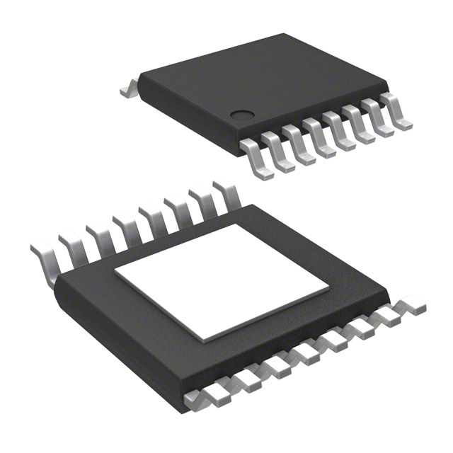
Designed for PWM (pulse width modulated) control of dc motors, the A3949 is capable of peak output currents to ±2.8 A and operating voltages to 36 V. PHASE and ENABLE input terminals are provided for use in controlling the speed and direction of a dc motor with externally applied PWM control signals. Internal synchronous rectification control circuitry is provided to reduce power dissipation during PWM operation. Internal circuit protection includes thermal shutdown with hysteresis, undervoltage monitoring of VBB and VCP , and crossover current protection. The A3949 is supplied in a choice of two power packages, a 16-pin plastic SOIC with a copper batwing tab (part number suffix LB), and a low profile (1.1mm) 16-pin TSSOP (suffix LP) with exposed power tab. Both packages are available in a lead-free version (100% matte tin leadframe).
Scale 1:1
OUTA SENSE
10 OUTB 9 VBB
A3949SLP TSSOP
N/C MODE PHASE GND SLEEP 1 2 3 4 5 6 7 8 16 N/C 15 VREG 14 VCP 13 GND 12 CP2 11 CP1 10 OUTB 9 VBB
Scale 1:1
ENABLE OUTA SENSE
FEATURES
Single supply operation Very small outline package Low RDS(ON) outputs Sleep function Internal UVLO Crossover current protection Thermal shutdown protection
ABSOLUTE MAXIMUM RATINGS
Load Supply Voltage VBB............................................................... 36 V VBB (Peak < 2 μs) ........................................38 V Output Current, IOUT (Repetitive)1 ....................±2.8 A Sense Voltage, VSENSE .........................................0.5 V Logic Input Voltage, VIN ......................–0.3 V to 7 V Package Power Dissipation, PD A3949SLB2 ......................................... 52ºC / W A3949SLP3.......................................... 34ºC / W Operating Temperature Range Ambient Temperature, TA ............ –20°C to +85°C Junction Temperature, TJ ................. +150°C Max. Storage Temperature, TS........... –55°C to +150°C Output current rating may be limited by duty cycle, ambient temperature, and heat sinking. Under any set of conditions, DO NOT exceed the specified IOUT or TJ. 2 Measured on a typical two-sided PCB with 2 in.2 copper ground plane. 3 Measured on a JEDEC-standard "High-K" 4-layer PCB.
1
Use the following complete part numbers when ordering:
Part Number A3949SLB-T A3949SLBTR-T A3949SLP-T A3949SLPTR-T
*
Pb-free* Yes Yes Yes Yes
Package 16-pin, SOIC 16-pin, SOIC 16-pin, TSSOP 16-pin, TSSOP
Packing 47 per tube 1000 per reel 96 per tube 4000 per reel
Pb-based variants are being phased out of the product line. The variants cited in this footnote are in production but have been determined to be LAST TIME BUY. This classification indicates that sale of this device is currently restricted to existing customer applications. The variants should not be purchased for new design applications because obsolescence in the near future is probable. Samples are no longer available. Status change: October 31, 2006. Deadline for receipt of LAST TIME BUY orders: April 27, 2007. These variants include: A3949SLB, A3949SLBTR, A3949SLP, and A3949SLPTR.
�Data Sheet 29319.47D
A3949 DMOS Full-Bridge Motor Driver
Functional Block Diagram
.22 μF 25 V VREG 0.1 μF CP1 CP2
Low Side Gate Supply
OSC
Charge Pump
VCP 0.1 μF VBB Load Supply
MODE 0.1 μF 100 μF
PHASE OUTA Control Logic ENABLE SENSE SLEEP DMOS Full Bridge GND GND OUTB
Control Logic Table
PHASE ENABLE MODE 1 0 X 1 0 X 1 1 0 0 0 X X X 1 0 0 X SLEEP 1 1 1 1 1 0 OUTA H L L L H Hi-Z OUTB L H L H L Hi-Z Function Forward Reverse Brake (slow decay) Fast decay SR* Fast decay SR* Sleep mode
* To prevent reversal of current during fast decay SR (synchronous rectification), the outputs go to the high impedance state as the current approaches zero.
www.allegromicro.com
115 Northeast Cutoff, Box 15036 Worcester, Massachusetts 01615-0036 (508) 853-5000
2
�Data Sheet 29319.47D
A3949 DMOS Full-Bridge Motor Driver
ELECTRICAL CHARACTERISTICS at TA = 25°C, VBB = 8 V to 36 V (unless otherwise noted)
Characteristics Symbol Test Conditions Source driver, IOUT = –2.8 A, TJ= 25°C Output-On Resistance RDSON Source driver, IOUT = –2.8 A, TJ= 125°C Sink driver, IOUT = 2.8 A, TJ= 25°C Sink driver, IOUT = –2.8 A, TJ= 125°C Body Diode Forward Voltage VF Source diode, IF = –2.8 A Sink diode, IF = 2.8 A fPWM < 50 kHz Motor Supply Current IBB Charge pump turned on; outputs disabled Sleep mode Logic Input Voltage PHASE, ENABLE, MODE Logic Input Voltage SLEEP Logic Input Current PHASE, MODE pins Logic Input Current ENABLE pin Logic Input Current SLEEP pin Propagation Delay Times Crossover Delay Protection Circuitry UVLO Enable Threshold UVLO Hysteresis Thermal Shutdown Temp. Thermal Shutdown Hysteresis TJ ΔTJ VBB rising – – – – 6 250 170 15 – – – – V mV °C °C VIN(1) VIN(0) VIN(1) VIN(0) IIN(1) IIN(0) IIN(1) IIN(0) IIN(1) IIN(0) tpd tCOD VIN = 2.0 V VIN = 0.8 V VIN = 2.0 V VIN = 0.8 V VIN = 2.7 V VIN = 0.8 V From PWM change to source or sink turn on From PWM change to source or sink turn off Min. – – – – – – – – – 2.0 – 2.7 – – – – – – – – – – Typ. .4 .68 .3 .576 1.1 1 6 3 – – – – – < 1.0 < –2.0 40 16 27
很抱歉,暂时无法提供与“A3949SLP-T”相匹配的价格&库存,您可以联系我们找货
免费人工找货