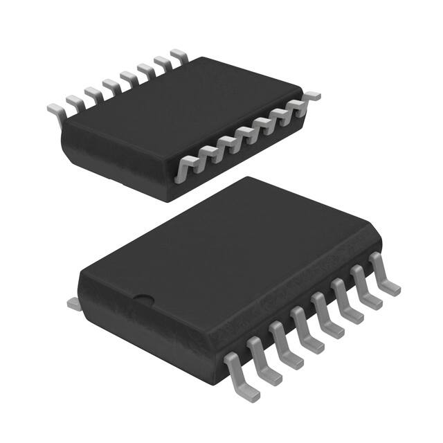
0
登录后你可以
  • 下载海量资料
  • 学习在线课程
  • 观看技术视频
  • 写文章/发帖/加入社区
会员中心
创作中心
发布
  • 发文章

  • 发资料

  • 发帖

  • 提问

  • 发视频

创作活动
A3955SLBTR-T

A3955SLBTR-T

  • 厂商:

    ALLEGRO(埃戈罗)

  • 封装:

    SOIC16

  • 描述:

    IC MTR DRV BIPLR 4.5-5.5V 16SOIC

  • 数据手册
  • 价格&库存
A3955SLBTR-T 数据手册
A3955 Full-Bridge PWM Microstepping Motor Driver Features and Benefits ▪ ±1.5 A continuous output current ▪ 50 V output voltage rating ▪ Internal PWM current control ▪ 3-bit nonlinear DAC ▪ Fast, mixed fast/slow, and slow current-decay modes ▪ Internal transient-suppression diodes ▪ Internal thermal shutdown circuitry ▪ Crossover-current and UVLO protection Description The A3955 is designed to drive one winding of a bipolar stepper motor in a microstepping mode. The outputs are rated for continuous output currents to ±1.5 A and operating voltages to 50 V. Internal pulse width modulated (PWM) current control combined with an internal three-bit nonlinear digitalto-analog converter allows the motor current to be controlled in full-, half-, quarter-, or eighth-step (microstepping) modes. Nonlinear increments minimize the number of control lines necessary for microstepping. Microstepping provides increased step resolution, and reduces torque variations and resonance problems at low speed. Internal circuitry determines whether the PWM current-control circuitry operates in a slow (recirculating) current-decay mode, fast (regenerative) current-decay mode, or in a mixed current-decay mode in which the off-time is divided into a period of fast current decay and with the remainder of the fixed off-time spent in slow current decay. The combination of user-selectable current-sensing resistor and reference voltage, digitally selected output current ratio; and slow, fast, or mixed current-decay modes provides users with a broad, variable range of motor control. Continued on the next page… Packages: Package B, 16-pin DIP with exposed tabs Not to scale Package LB, 16-pin SOIC with internally fused pins Functional Block Diagram LOGIC SUPPLY LOAD SUPPLY OUTA OUTB PHASE 7 6 VCC 10 15 16 VBB GROUND 4 5 12 13 UVLO & TSD MIXED-DECAY COMPARATOR PWM LATCH BLANKING GATE CURRENT-SENSE COMPARATOR SENSE 11 PFD 1 + – BLANKING R Q S +– RC 3 V TH 2 REF + – ÷3 D/A DISABLE VCC RS 8 D2 9 D1 14 D0 RT CT Dwg. FP-042 29319.41E A3955 Description (continued) Full-Bridge PWM Microstepping Motor Driver Internal circuit protection includes thermal shutdown with hysteresis, transient-suppression diodes, and crossover-current protection. Special power-up sequencing is not required. The A3955 is supplied in a choice of two power packages; a 16-pin dual-in-line plastic package with copper heat-sink tabs (suffix ‘B’), Selection Guide Part Number A3955SB-T A3955SLB-T A3955SLBTR-T and a 16-lead plastic SOIC with internally fused pins (suffix ‘LB’). For both package styles, the thermally enhanced pins are at ground potential and need no electrical isolation. Both packages are lead (Pb) free, with leadframe plating 100% matte tin. Packing 16-pin DIP with exposed thermal tabs 16-pin SOICW with internally fused pins 16-pin SOICW with internally fused pins Package 25 per tube 47 per tube 1000 per reel Absolute Maximum Ratings Characteristic Load Supply Voltage Logic Supply Voltage Logic/Reference Input Voltage Range Sense Voltage Output Current, Continuous Package Power Dissipation Operating Ambient Temperature Maximum Junction Temperature Storage Temperature Symbol VBB VCC VIN VS IOUT PD TA TJ(max) Tstg Range S Fault conditions that produce excessive junction temperature will activate the device’s thermal shutdown circuitry. These conditions can be tolerated but should be avoided. Output current rating may be limited by duty cycle, ambient temperature, and heat sinking. Under any set of conditions, do not exceed the specified current rating or a junction temperature of 150°C. Notes Rating 50 7.0 –0.3 to VCC + 0.3 1.0 ±1.5 See graph –20 to 85 150 –55 to 150 Units V V V V mA W ºC ºC ºC Thermal Characteristics Characteristic Package Thermal Resistance, Junction to Ambient Package Thermal Resistance, Junction to Tab Symbol RθJA Test Conditions* 2 B Package, single-layer PCB, 1 in. 2-oz. exposed copper Value 43 67 6 Units ºC/W ºC/W ºC/W LB Package, 2-layer PCB, 0.3 side 2 in. 2-oz. exposed copper each RθJT *Additional thermal information available on Allegro website. ALLOWABLE PACKAGE POWER DISSIPATION (W) 4 R θJT = 6.0°C/W 3 SUFFIX 'B', R θJA = 43°C/W 2 1 SUFFIX 'LB', R θJA = 67°C/W 0 25 50 75 100 TEMPERATURE IN °C 125 150 Allegro MicroSystems, Inc. 115 Northeast Cutoff Worcester, Massachusetts 01615-0036 U.S.A. 1.508.853.5000; www.allegromicro.com 2 A3955 Full-Bridge PWM Microstepping Motor Driver ELECTRICAL CHARACTERISTICS at TA = 25°C, VBB = 5 V to 50 V, VCC = 4.5 V to 5.5 V (unless otherwise noted.) Limits Characteristic Symbol Test Conditions Min. Typ. Max. Units Power Outputs Load Supply Voltage Range Output Leakage Current VBB ICEX VCE(SAT) Operating, IOUT = ±1.5 A, L = 3 mH VOUT = VBB VOUT = 0 V Output Saturation Voltage (Forward or Reverse Mode) VS = 1.0 V: Source Driver, IOUT = -0.85 A Source Driver, IOUT = -1.5 A Sink Driver, IOUT = 0.85 A Sink Driver, IOUT = 1.5 A Sense Current Offset Clamp Diode Forward Voltage (Sink or Source) Motor Supply Current (No Load) ISO VF IBB(ON) IBB(OFF) D0 = D1 = D2 = 0.8 V IS - IOUT, IOUT = 850 mA, VS = 0 V, VCC = 5 V IF = 0.85 A IF = 1.5 A — — — — 20 — — — — 1.0 1.3 0.5 1.3 33 1.2 1.4 2.0 1.0 1.2 1.5 0.6 1.5 40 1.4 1.7 4.0 50 V V V V mA V V mA μA VCC — — —
A3955SLBTR-T 价格&库存

很抱歉,暂时无法提供与“A3955SLBTR-T”相匹配的价格&库存,您可以联系我们找货

免费人工找货